EP1184980A2 - Digital receiver - Google Patents
Digital receiver Download PDFInfo
- Publication number
- EP1184980A2 EP1184980A2 EP01306378A EP01306378A EP1184980A2 EP 1184980 A2 EP1184980 A2 EP 1184980A2 EP 01306378 A EP01306378 A EP 01306378A EP 01306378 A EP01306378 A EP 01306378A EP 1184980 A2 EP1184980 A2 EP 1184980A2
- Authority
- EP
- European Patent Office
- Prior art keywords
- digital
- output data
- delay element
- multiplier
- adder
- Prior art date
- Legal status (The legal status is an assumption and is not a legal conclusion. Google has not performed a legal analysis and makes no representation as to the accuracy of the status listed.)
- Withdrawn
Links
- 238000005070 sampling Methods 0.000 claims abstract description 72
- 238000001514 detection method Methods 0.000 claims abstract description 33
- 238000001914 filtration Methods 0.000 claims abstract description 17
- 238000006243 chemical reaction Methods 0.000 claims abstract 5
- 230000001934 delay Effects 0.000 claims 14
- 238000005457 optimization Methods 0.000 description 7
- 238000000034 method Methods 0.000 description 5
- 238000010586 diagram Methods 0.000 description 3
- 230000001172 regenerating effect Effects 0.000 description 3
- 102220079670 rs759826252 Human genes 0.000 description 2
- 230000002238 attenuated effect Effects 0.000 description 1
- 230000000694 effects Effects 0.000 description 1
- 230000002194 synthesizing effect Effects 0.000 description 1
Images



Classifications
-
- H—ELECTRICITY
- H03—ELECTRONIC CIRCUITRY
- H03H—IMPEDANCE NETWORKS, e.g. RESONANT CIRCUITS; RESONATORS
- H03H17/00—Networks using digital techniques
- H03H17/02—Frequency selective networks
- H03H17/04—Recursive filters
- H03H17/0416—Recursive filters with input-sampling frequency and output-delivery frequency which differ, e.g. extrapolation; Anti-aliasing
Definitions
- the present invention relates to a receiver for regenerating a signal wave from a received wave, and in particular to a receiver for regenerating a signal wave via digital signal processing.
- an analog receiver of the superheterodyne system is known as a receiver for receiving a broadcast wave transmitted from a broadcast station and regenerating a signal wave in the audio frequency band.
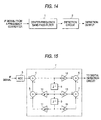
- the analog receiver converts a broadcast wave to an IF signal of the intermediate frequency and removes unwanted frequency components bypassing the IF signal through a band-pass filter 1 the intermediate frequency band as shown in Fig. 14, and obtains a signal wave (detection output) via a detection circuit 2.
- the inventor of the application has formed the aforementioned analog receiver via digital circuits to make an attempt to develop a digital receiver that is compatible with for example digital audio apparatus.
- the inventor of the application has proposed that the band-pass filter shown in Fig. 14 includes a direct-type secondary IIR (infinite Impulse response) filter 1' shown in Fig. 15 and that a detection circuit subordinate to the digital band-pass filter 1' be digitized. That is, the inventor has proposed that the digital band-pass filter 1' includes digital adders 4, 5, 6, 7, digital delay elements 8, 9, and digital multipliers 10, 11, 12, 13, 14, and that digital data generated by converting an IF signal from a frequency converter undergo digital filtering.
- IIR infinite Impulse response
- an IF signal is down-converted by a frequency converter, it is a signal prior to detection.
- using an IIR filter of a general configuration in Fig. 15 requires use of a large-scale digital circuit that allows high-speed arithmetic operation, making application to a receiver difficult.
- the invention has been proposed to solve such problems involved in the related art and aims at providing a new receiver of a simple configuration that can allows high-accuracy digital signal processing.
- the invention is a receiver comprising digital signal processing section for transmitting data corresponding to a desired frequency component from digital data in the intermediate frequency band to output the data to detection section, characterized in that the digital signal processing section comprises a digital band-pass filter for performing digital filtering on the digital data at a first sampling rate equal to an exponentiation multiple of 2 of the intermediate frequency and an interpolation filter including a digital low pass filter for performing digital filtering on the data output from the digital band-pass filter at a second sampling rate equal to an exponentiation multiple of 2 of the intermediate frequency, the second sampling rate higher than the first sampling rate, and that the output data of the interpolation filter is output to the detection section.
- the digital signal processing section comprises a digital band-pass filter for performing digital filtering on the digital data at a first sampling rate equal to an exponentiation multiple of 2 of the intermediate frequency and an interpolation filter including a digital low pass filter for performing digital filtering on the data output from the digital band-pass filter at a second sampling rate equal to an exponentiation multiple of 2
- the receiver is characterized in that the first sampling rate is set to four times the intermediate frequency and that the digital band-pass filter includes an IIR filter whose multiplicand attribute is set to the value of an exponentiation multiple of 2.
- the receiver is characterized in that the second sampling rate is set to 16 times the intermediate frequency and that the interpolation filter includes an IIR filter whose multiplicand attribute is set to the value of an exponentiation multiple of 2.
- the digital band-pass filter performs digital filtering on data in the intermediate frequency band at a first sampling rate equal to an exponentiation multiple of 2 of the intermediate frequency (a sampling rate lower than a second sampling rate) and the interpolation filter performs digital filtering on data output from the digital band-pass filter at a second sampling rate equal to an exponentiationmultiple of 2 of the intermediate frequency, the second sampling rate higher than the first sampling rate, to output the data from the interpolation filter to the detection section.
- the circuit scale of the digital band-pass filter and the interpolation filter can be simplified. That is, operating a digital band-pass filter at a low sampling rate makes it possible to simplify the circuit scale of the digital band-pass filter. Even in a configuration where an interpolation filter operating at a higher sampling rate is used together with the simplified digital band-pass filter, it is possible to further simplify the overall circuit scale than in a case where a digital band-pass filter of a general configuration is operated at a high sampling rate.
- data processed at a lower sampling rate by a digital band-pass filter is then processed at a higher sampling rate by an interpolation filter in order to upgrade the detection accuracy in detection section.
- a receiver In order for detection section to perform high-accuracy detection, it is desirable to detect waves based on data processed at a high sampling rate.
- a receiver provides both the simple circuit scale and the high-accuracy detection by a combination of a digital band-pass filter operating at a lower sampling rate and an interpolation filter operating at a higher sampling rate.
- the first sampling rate of the digital band-pass filter to an exponentiation multiple of 2 of (in particular four times) the intermediate frequency and the second sampling rate of the interpolation filter to an exponentiation multiple of 2 of (in particular 16 times) the intermediate frequency
- it is possible to approximate, by using an exponentiation multiple of 2 the multiplicand attribute of an IIR filter that includes the digital band-pass filter and the interpolation filter respectively. This simplifies the circuit scale of a digital multiplier.
- FIG. 1 is a block diagram showing the key configuration of an exemplary receiver for receiving an AM broadcast wave according to this embodiment.
- the receiver down-converts an AM broadcast wave received at an antenna ANT to an IF signal S IF of the intermediate frequency (455 kHz) via a frequency converter including a mixer MIX and a local oscillator L.OSC, converts the analog IF signal S IF to digital data D IF via an A/D converter 15, then passes the digital data D IF through a digital signal processing circuit consisting of a digital band-pass filter 16 and an interpolation filter 17 supply the resulting data to a digital detection circuit 18.
- the sampling frequency f s0 of the A/D converter 15 is set to above four times the intermediate frequency f 0
- the sampling rate f s1 of the digital band-pass filter 16 is set to four times the intermediate frequency f 0
- the sampling rate f s2 of the interpolation filter 17 is set to 16 times the intermediate frequency f 0 , thus satisfying Nyquist sampling theorem.
- the A/D converter 15 converts the analog IF signal S IF to 16-bit digital data D IF .
- the digital band-pass filter 16 and the interpolation filter 17 perform 16-bit digital signal processing on the digital data D IF .
- the digital band-pass filter 16 is a direct-type second IIR filter and implemented as a direct-type secondary III filter shown in Fig. 2 or as a direct-type secondary III filter shown in Fig. 3, depending on the design specifications.
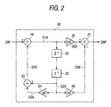
- the digital band-pass filter 16 shown in Fig. 2 including a plurality of digital adders 19, 20, 21, digital delay elements 22, 23, and digital multipliers 24, 25, 26.
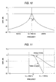
- the digital band-pass filter 16 is an IIR filter having single-peak characteristics where the maximum gain is obtained at the center frequency f 0 (455 kHz) as shown in Fig. 10.
- the bandwidth of the single-peak characteristics (6-dB bandwidth) ⁇ F around the center frequency f 0 (455 kHz) is set to a width to allow an upper sideband wave and a lower sideband wave of the IF signal S IF to pass through the bandwidth and the Q value (f 0 / ⁇ F) is set to characteristics that meet a particular need.
- the digital band-pass filter 16 shown in Fig. 3 including two serially connected IIR filters 16a, 16b, each of which including a plurality of digital adders 19, 20, 201, digital delay elements 22, 23, and digital multipliers 24, 25, 26, 202.
- the IIR filters 16a and 16b differ from each other in that the digital adder provided in the IIR filter 16a performs subtraction D202-D20 on the data D202, D20 provided by the digital multipliers 202, 20.
- the digital adder provided in the IIR filter 16b performs subtraction -D20-D202 on the data D202, D20 provided by the digital multipliers 202, 20.
- the digital band-pass filter 16 shown in Fig. 3 comprising two serially connected IIR filters 16a, 16b have twin-peak characteristics around the center frequency f 0 (455kHz).
- the bandwidth of the twin-peakcharacteristics (6-dB bandwidth) ⁇ F around the center frequency f 0 (455 kHz) is set to a width to allow an upper sideband wave and a lower sideband wave of the IF signal S IF to pass through the bandwidth and the Q value (f 0 / ⁇ F) is set to characteristics that meet a particular need.
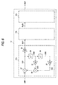
- the interpolation filter includes three IIR filters of the same configuration 17a, 17b, 17c as shown in Fig. 6.
- the IIR filter 17a includes a plurality of digital adders 27, 28, digital delay elements 29, 30, and digital multipliers 31, 32, 33.
- the remaining IIR filters have the same configuration as the IIR filter 17a.
- frequency characteristics is implemented where the gain in the high frequencies above the cutoff frequency F c is suddenly attenuated by synthesizing the frequency characteristics of three stages of IIR filters 17a, 17b, 17c.
- the cutoff frequency of each of the IIR filters 17a, 17b, 17c is set to a frequency higher than the center frequency f 0 (455 kHz).
- the cutoff frequency is set to obtain a passband to pass an upper sideband wave of the IF signal S IF .
- H(z) z-converted as shown in the next expression (1) is applied to the band-pass filter 16 shown in Fig. 2.
- H(z) (b0+b1 ⁇ z -1 +b2 ⁇ z -2 )/(1-a1 ⁇ z -1 +a2 ⁇ z -2 )
- a direct-type secondary IIR filter shown in Fig. 15 is assumed based on this transfer function H(z) and the optimum value of each of the multiplicand attributes a1, a2, b0, b1 and b2 of the transfer function H(z).
- each of the multiplicand attributes a1, a2, b0, b1 and b2 is optimized under the optimization conditions that the digital band-pass filter is implemented via a simple configuration, considering the relationship between the sampling rate f s1 and the intermediate frequency f 0 (455 kHz) and Q value.
- each of the multiplicand attributes a1, a2, b0, b1 and b2 is as shown in the next expression (2), especially, both multiplicand attributes a1 and b1 being set to 0.
- the digital band-pass filter 16 shown in Fig. 2 has a configuration where digital multipliers 10, 13 and digital adders 5, 7 in Fig. 15 are omitted as well as a combination of a digital multiplier 24 and a new digital adder 20 is used to generate data D20 to be supplied to the digital adder 19, thus further reducing the circuit scale.
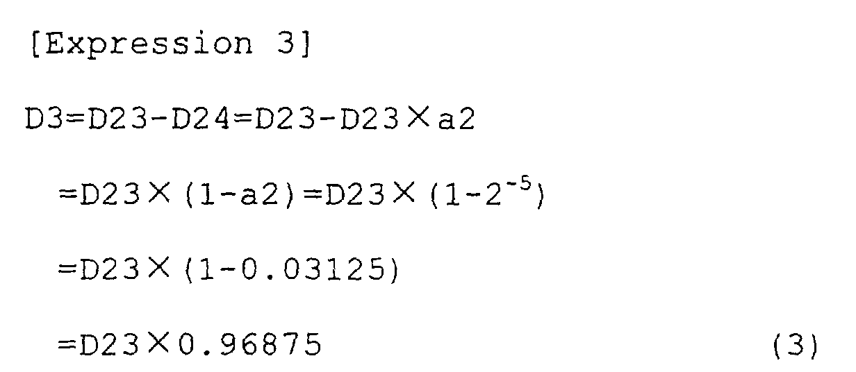
- the circuit scale can be made smaller than via the IIR filter 1' shown in Fig. 15. Note that, since the multiplicand attribute a2 is a fraction having a large number of digits, having the digital multiplier 24 alone perform the arithmetic operation (0.96721311 ⁇ D23) requires a complicated digital multiplier with a large circuit scale.
- a combination of the digital multiplier 24 and the digital adder 20 is used to substantially perform the arithmetic operation (0.96721311 ⁇ D23) to allow reduction of the circuit scale.
- a digital multiplier 24 may be a simple digital multiplier. Further, since a digital adder 20 performs simple subtraction, the digital adder 20 may be a simple digital adder. As a result, adding a digital adder 20 to a digital multiplier 24 reduces the circuit scale compared with providing a digital multiplier alone to perform complicated arithmetic operation.
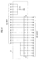
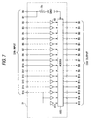
- a decoder circuit shown in Fig. 4 is applied to effectuate the reduction of the circuit scale.
- the digital multiplier 24 shown in Fig. 4 outputs bits B5 to B15 of the input data D23 as bits B0 to B10 of the output data D24, as well as outputs bit B15 of the input data D23 as bits B10 to B15 of the output data D24. Bits B0 to B4 of the input data D23 are pulled down to the ground GND via a resistor R1 and the output data D24 (B15 to B0) is output via buffer amplifiers A15 to A0.
- the multiplicand attribute b0 of the digital multiplier 25 is determined as follows.
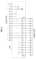
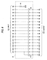
- the digital multiplier 25 shown in Fig. 5 outputs bits B6 to B15 of the input data D19 as bits B0 to B10 of the output data D25, as well as outputs bit B15 of the input data D19 as bits B9 to B15 of the output data D25.
- Bits B0 to B5 of the input data D19 are pulled down to the ground GND via a resistor R1 and the output data D25 (B15 to B0) is output via buffer amplifiers A15 to A0.
- the multiplicand attribute b0 of the digital multiplier 26 in Fig. 2 is determined as follows.
- an IIR filter having frequency characteristics shown in Fig. 10 is implemented via a simple configuration.
- Apre-stage filter 16a and a post-stage filter 16b are both provided in variation of the digital band-pass filter 16 shown in Fig. 2.
- the transfer function H(z) shown in Expression (1) is applied.
- a direct-type secondary IIR filter shown in Fig. 15 is considered based on the transfer function H(z) .
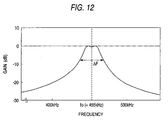
- the optimum value of each of the multiplicand attributes a1, a2, b0, b1, b2 is obtained in order to acquire the frequency characteristics show in Fig. 12.
- optimization of each of the multiplicand attributes a1, a2, b0, b1, b2 is carried out while considering the relationship between the sampling rate f s1 for digital filtering, the intermediate frequency f 0 , and the Q value.
- a digital adder 201 and a digital multiplier 202 are added to the filter 16a and the filter 16b shown in Fig. 3, respectively.
- connection is made so that the output data D202 of the digital multiplier 201 is supplied to the addition input terminal (plus terminal) of the digital adder 201 in the filter 16a, the output data D20 of the digital adder 20 is supplied to the subtraction input terminal (minus terminal) of the digital adder 201, the output data D202 of the digital multiplier 202 is supplied to the subtraction input terminal (minus terminal) of the digital adder 201 in the filter 16b, and the output data D20 of the digital adder 20 is supplied to the subtraction input terminal (minus terminal) of the digital adder 201
- a digital band-pass filter having twin-peak characteristics shown in Fig. 12 is formed.
- the digital multiplier 202 in the filter 16a and the digital multiplier 202 in the filter 16 can be configured by a decoder circuit shown in Fig. 4 or 5 in order to implement a simple configuration.
- an IIR filter having frequency characteristics shown in Fig. 12 is implemented via a simple configuration.
- a combination of digital band-pass filters having different center frequencies can provide desired characteristics.
- a pre-stage filter 17a, a middle-stage filter 17b and a post-stage filter 17c in Fig. 6 have the same configuration.
- the configuration method of the pre-stage filter 17a will be described as a representative.
- the digital band-bass filter 16 performs digital filtering based on the sampling rate f s1 four times the center frequency f 0 to output data D BF .
- the data D BF indicates data at four sampling points P1 to P4 in one cycle (1/f 0 ) as the reciprocal of the intermediate frequency f 0 .
- Data D BF appearing at four sampling points P1 to P4 in one cycle (1/f 0 ) does not assure high-accuracy detection since the detection output level varies considerably even when data D BF is supplied to a digital detection circuit 18 for detection when the phases of the sampling points P1 to P4 are dislocated, such as in the case of Figs. 13A and 13B.
- an interpolation filter 17 including a digital low pass filter is provided between the digital band-bass filter 16 and the digital detection circuit 18.
- the multiplicand attributes a1, a2, b0 becomes 2 -2 , 2 -1 and 2 -2 , respectively.
- the multiplicand attribute a1 of the digital multiplier 31 in the filter 17a is fixed to 2 -2
- the multiplicand attribute a2 of the digital multiplier 32 to 2 -2 is fixed to 2 -2
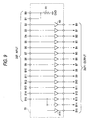
- the multiplicand attribute b0 of the digital multiplier 33 to 2 -2 is fixed to 2 -2 .
- the digital multiplier 31 is configured by a decoder circuit shown in Fig. 7, the digital multiplier 32 by a decoder circuit shown in Fig. 8, and the digital multiplier 33 by a decoder circuit shown in Fig. 9 respectively in order to implement each digital multiplier 31, 32, 33 via a simple configuration.
- filters 17b, 17c same as a filter 17a, an interpolation filter 17 having frequency characteristics shown in Fig. 11 is implemented.
- the circuit scale is simplified by operating the digital band-pass filter 16 at the sampling rate f s1 four times the intermediate frequency f c (low sampling rate).
- the interpolation filter 17 is operated at the sampling rate f s2 16 times the intermediate frequency f c (high sampling rate) and the resulting data D LF of the high sampling rate is supplied to the digital detection circuit 18.
- the circuit scale can be simplified compared with the IIR filter 1' in a general configuration shown in Fig. 15 as well as high-accuracy detection is allowed.
- digital multipliers 24, 25, 26, 202, 31, 32, 33 are configured by decoder circuits as shown in Figs. 4, 5, 7, 8 and 9, the invention is not limited to such a configuration.
- Digital multipliers 24, 25, 26, 202, 31, 32, 33 may be configured via binary shift registers that allow bit shift operation.
- AM receiver is addressed in this embodiment, the invention can be applied to other receivers such as FM receivers.
- a receiver comprises a digital band-pass filter for performing digital filtering on the digital data at a first sampling rate equal to an exponentiation multiple of 2 of the intermediate frequency and a digital interpolation filter for performing digital filtering on the data output from the digital band-pass filter at a second sampling rate equal to an exponentiation multiple of 2 of the intermediate frequency.
Landscapes
- Physics & Mathematics (AREA)
- Engineering & Computer Science (AREA)
- Computer Hardware Design (AREA)
- Mathematical Physics (AREA)
- Complex Calculations (AREA)
- Digital Transmission Methods That Use Modulated Carrier Waves (AREA)
- Superheterodyne Receivers (AREA)
- Circuits Of Receivers In General (AREA)
- Analogue/Digital Conversion (AREA)
- Transmission Systems Not Characterized By The Medium Used For Transmission (AREA)
- Measuring Frequencies, Analyzing Spectra (AREA)
Abstract
Description

is implemented.
Claims (16)
- A receiver comprising digital signal processing means for transmitting data corresponding to a desired frequency component from digital data in the intermediate frequency band to output the data to detection means, whereinsaid digital signal processing means comprises:a digital band-pass filter for performing digital filtering on the digital data at a first sampling rate equal to an exponentiation multiple of 2 of the intermediate frequency andan interpolation filter including a digital low pass filter for performing digital filtering on the data output from said digital band-pass filter at a second sampling rate equal to an exponentiation multiple of 2 of the intermediate frequency, the second sampling rate higher than the first sampling rate, and whereinthe output data of said interpolation filter is output to said detection means.
- The receiver according to claim 1, whereinthe first sampling rate is set to four times the intermediate frequency, andsaid digital band-pass filter includes an IIR filter whose multiplicand attribute is set to the value of an exponentiation multiple of 2.
- The receiver according to claim 1, whereinthe second sampling rate is set to 16 times the intermediate frequency, andsaid interpolation filter includes an IIR filter whose multiplicand attribute is set to the value of an exponentiation multiple of 2.
- The receiver according to claim 1, whereinsaid digital band-pass filter comprises:a first, a second, and a third digital adders,a first, a second, and a third digital multipliers, anda digital delay element having a delay time twice that for the first sampling rate,said first digital adder subtracts output data of said second digital adder from the digital data output from analog-to-digital conversion means,said digital delay element delays output data of said first digital adder,said first digital multiplier multiplies output data of said digital delay element by a first predetermined multiplicand attribute,said second digital adder subtracts output data of said first digital multiplier from output data of said digital delay element,said second digital multiplier multiplies output data of said first digital adder by a second predetermined multiplicand attribute,said third digital multiplier multiplies output data of said digital delay element by a second predetermined multiplicand attribute, andsaid third digital adder subtracts output data of said third digital multiplier from output data of said second digital multiplier and outputs the subtraction results to said interpolation filter.
- The receiver according to claim 1, whereinsaid digital band-pass filter comprises:a first filter means includes;a first, a second, a third, and a fourth digital adders,a first, a second, a third, and a fourth digital multipliers, anda first and a second digital delay elements serially connected, said elements having a delay time equal to that for the first sampling rate, anda second filter means includes;a fifth, a sixth, a seventh, and an eighth digital adders,a fifth, a sixth, a seventh, and an eighth digital multipliers, anda third and a fourth digital delay elements serially connected, said elements having a delay time equal to that for the first sampling rate,said first digital adder subtracts output data of said second digital adder from the digital data output from said analog-to-digital conversion means,said first digital delay element delays output data of said first digital adder,said second digital delay element delays output data of said first digital delay element,said first digital multiplier multiplies output data of said first digital delay element by a first predetermined multiplicand attribute,said second digital adder subtracts output data of said third digital adder from output data of said first digital multiplier,said second digital multiplier multiplies output data of said second digital delay element by a second predetermined multiplicand attribute,said third digital adder subtracts output data of said third digital multiplier from output data of said second digital delay element,said third digital multiplier multiplies output data of said first digital adder by a third predetermined multiplicand attribute,said fourth digital multiplier multiplies output data of said second digital delay element by a second predetermined multiplicand attribute,said fourth digital adder subtracts output data of said fourth digital multiplier from output data of said third digital multiplier,said fifth digital adder adds output data of said sixth digital adder to output data of said fourth digital multiplier,said third digital delay element delays output data of said fifth digital adder,said fourth digital delay element delays output data of said third digital delay element,said fifth digital multiplier multiplies output data of said third digital delay element by a first predetermined multiplicand attribute,said sixth digital adder subtracts output data of said fifth digital multiplier from output data of said seventh digital adder,said sixth digital multiplier multiplies output data of said fourth digital delay element by a second predetermined multiplicand attribute,said seventh digital adder subtracts output data of said sixth digital multiplier from output data of said fourth digital delay element,said third digital multiplier multiplies output data of said fifth digital adder by a seventh predetermined multiplicand attribute,said eighth digital multiplier multiplies output data of said fourth digital delay element by a second predetermined multiplicand attribute, andsaid eighth digital adder subtracts output data of said eighth digital multiplier from output data of said seventh digital multiplier and outputs the subtraction results to said interpolation filter.
- The receiver according to claim 1, whereinsaid interpolation filter comprises:a low pass filter means including;a ninth, and a tenth digital adders,a ninth, a tenth, and an eleventh digital multipliers, anda fifth, and a sixth digital delay elements serially connected, said elements having a delay time equal to that for the second sampling rate,said ninth digital adder adds data supplied from said digital band-pass filter and output data of said tenth digital adder,said fifth digital delay element delays output data of said ninth digital adder,said sixth digital delay element delays output data of said fifth digital delay element,said ninth digital multiplier multiplies output data of said fifth digital delay element by a ninth predetermined multiplicand attribute,said tenth digital adder subtracts output data of said tenth digital multiplier from output data of said ninth digital multiplier,said tenth digital multiplier multiplies output data of said sixth digital delay element by a tenth predetermined multiplicand attribute, andsaid eleventh digital multiplier multiplies output data of said ninth digital delay element by an eleventh predetermined multiplicand attribute and outputs the multiplication results to said detection means.
- The receiver according to claim 1, whereinsaid interpolation filter includes a plurality of said low pass filter means serially connected.
- The receiver according to claim 6, whereinthe ninth and the eleventh multiplicand attributes of said ninth and said eleventh digital multiplier are set to 2-2, andthe tenth multiplicand attribute of said tenth digital multiplier are set to 2-1.
- A receiver comprising digital signal processing section for transmitting data corresponding to a desired frequency component from digital data in the intermediate frequency band to output the data to detection section, whereinsaid digital signal processing section comprises:a digital band-pass filter for performing digital filtering on the digital data at a first sampling rate equal to an exponentiation multiple of 2 of the intermediate frequency andan interpolation filter including a digital low pass filter for performing digital filtering on the data output from said digital band-pass filter at a second sampling rate equal to an exponentiation multiple of 2 of the intermediate frequency, the second sampling rate higher than the first sampling rate, and whereinthe output data of said interpolation filter is output to said detection section.
- The receiver according to claim 9, whereinthe first sampling rate is set to four times the intermediate frequency, andsaid digital band-pass filter includes an IIR filter whose multiplicand attribute is set to the value of an exponentiation multiple of 2.
- The receiver according to claim 9, whereinthe second sampling rate is set to 16 times the intermediate frequency, andsaid interpolation filter includes an IIR filter whose multiplicand attribute is set to the value of an exponentiation multiple of 2.
- The receiver according to claim 9, whereinsaid digital band-pass filter comprises:a first, a second, and a third digital adders,a first, a second, and a third digital multipliers, anda digital delay element having a delay time twice that for the first sampling rate,said first digital adder subtracts output data of said second digital adder from the digital data output from analog-to-digital conversion section,said digital delay element delays output data of said first digital adder,said first digital multiplier multiplies output data of said digital delay element by a first predetermined multiplicand attribute,said second digital adder subtracts output data of said first digital multiplier from output data of said digital delay element,said second digital multiplier multiplies output data of said first digital adder by a second predetermined multiplicand attribute,said third digital multiplier multiplies output data of said digital delay element by a second predetermined multiplicand attribute, andsaid third digital adder subtracts output data of said third digital multiplier from output data of said second digital multiplier and outputs the subtraction results to said interpolation filter.
- The receiver according to claim 9, whereinsaid digital band-pass filter comprises:a first filter section includes;a first, a second, a third, and a fourth digital adders,a first, a second, a third, and a fourth digital multipliers, anda first and a second digital delay elements serially connected, said elements having a delay time equal to that for the first sampling rate, and
a second filter section includes;a fifth, a sixth, a seventh, and an eighth digital adders,a fifth, a sixth, a seventh, and an eighth digital multipliers, anda third and a fourth digital delay elements serially connected, said elements having a delay time equal to that for the first sampling rate,said first digital adder subtracts output data of said second digital adder from the digital data output from said analog-to-digital conversion section,said first digital delay element delays output data of said first digital adder,said second digital delay element delays output data of said first digital delay element,said first digital multiplier multiplies output data of said first digital delay element by a first predetermined multiplicand attribute,said second digital adder subtracts output data of said third digital adder from output data of said first digital multiplier,said second digital multiplier multiplies output data of said second digital delay element by a second predetermined multiplicand attribute,said third digital adder subtracts output data of said third digital multiplier from output data of said second digital delay element,said third digital multiplier multiplies output data of said first digital adder by a third predetermined multiplicand attribute,said fourth digital multiplier multiplies output data of said second digital delay element by a second predetermined multiplicand attribute,said fourth digital adder subtracts output data of said fourth digital multiplier from output data of said third digital multiplier,said fifth digital adder adds output data of said sixth digital adder to output data of said fourth digital multiplier,said third digital delay element delays output data of said fifth digital adder,said fourth digital delay element delays output data of said third digital delay element,said fifth digital multiplier multiplies output data of said third digital delay element by a first predetermined multiplicand attribute,said sixth digital adder subtracts output data of said fifth digital multiplier from output data of said seventh digital adder,said sixth digital multiplier multiplies output data of said fourth digital delay element by a second predetermined multiplicand attribute,said seventh digital adder subtracts output data of said sixth digital multiplier from output data of said fourth digital delay element,said third digital multiplier multiplies output data of said fifth digital adder by a seventh predetermined multiplicand attribute,said eighth digital multiplier multiplies output data of said fourth digital delay element by a second predetermined multiplicand attribute, andsaid eighth digital adder subtracts output data of said eighth digital multiplier from output data of said seventh digital multiplier and outputs the subtraction results to said interpolation filter. - The receiver according to claim 9, whereinsaid interpolation filter comprises:a low pass filter section including;a ninth, and a tenth digital adders,a ninth, a tenth, and an eleventh digital multipliers, anda fifth, and a sixth digital delay elements serially connected, said elements having a delay time equal to that for the second sampling rate,said ninth digital adder adds data supplied from said digital band-pass filter and output data of said tenth digital adder,said fifth digital delay element delays output data of said ninth digital adder,said sixth digital delay element delays output data of said fifth digital delay element,said ninth digital multiplier multiplies output data of said fifth digital delay element by a ninth predetermined multiplicand attribute,said tenth digital adder subtracts output data of said tenth digital multiplier from output data of said ninth digital multiplier,said tenth digital multiplier multiplies output data of said sixth digital delay element by a tenth predetermined multiplicand attribute, andsaid eleventh digital multiplier multiplies output data of said ninth digital delay element by an eleventh predetermined multiplicand attribute and outputs the multiplication results to said detection section.
- The receiver according to claim 14, whereinsaid interpolation filter includes a plurality of said low pass filter section serially connected.
- The receiver according to claim 14, whereinthe ninth and the eleventh multiplicand attributes of said ninth and said eleventh digital multiplier are set to 2-2, andthe tenth multiplicand attribute of said tenth digital multiplier are set to 2-1.
Applications Claiming Priority (2)
| Application Number | Priority Date | Filing Date | Title |
|---|---|---|---|
| JP2000230356 | 2000-07-31 | ||
| JP2000230356A JP2002043965A (en) | 2000-07-31 | 2000-07-31 | Receiver |
Publications (2)
| Publication Number | Publication Date |
|---|---|
| EP1184980A2 true EP1184980A2 (en) | 2002-03-06 |
| EP1184980A3 EP1184980A3 (en) | 2003-01-15 |
Family
ID=18723328
Family Applications (1)
| Application Number | Title | Priority Date | Filing Date |
|---|---|---|---|
| EP01306378A Withdrawn EP1184980A3 (en) | 2000-07-31 | 2001-07-25 | Digital receiver |
Country Status (3)
| Country | Link |
|---|---|
| US (1) | US6956911B2 (en) |
| EP (1) | EP1184980A3 (en) |
| JP (1) | JP2002043965A (en) |
Cited By (1)
| Publication number | Priority date | Publication date | Assignee | Title |
|---|---|---|---|---|
| WO2008075268A1 (en) * | 2006-12-19 | 2008-06-26 | Koninklijke Philips Electronics N.V. | Mri system with direct digital receiver using resampling |
Families Citing this family (6)
| Publication number | Priority date | Publication date | Assignee | Title |
|---|---|---|---|---|
| US6961395B2 (en) * | 2001-11-16 | 2005-11-01 | Nortel Networks Limited | Time variant filter implementation |
| US7971225B2 (en) * | 2002-02-08 | 2011-06-28 | Finisar Corporation | Bandpass component decimation and transmission of data in cable television digital return path |
| JP4836041B2 (en) * | 2006-01-27 | 2011-12-14 | エスティー‐エリクソン、ソシエテ、アノニム | Method and apparatus for sampling an RF signal |
| JP2007274217A (en) * | 2006-03-30 | 2007-10-18 | Sharp Corp | OFDM demodulation apparatus, OFDM demodulation method, program, and computer-readable recording medium |
| CN102946229B (en) * | 2012-10-23 | 2016-01-06 | 三维通信股份有限公司 | A kind of implementation method of Digital Down Convert |
| JP6686617B2 (en) * | 2016-03-28 | 2020-04-22 | Tdk株式会社 | Radiated emission measuring device |
Family Cites Families (9)
| Publication number | Priority date | Publication date | Assignee | Title |
|---|---|---|---|---|
| US4185325A (en) * | 1978-02-27 | 1980-01-22 | Appel Jean G | Recursive digital filter having coefficients equal to sums of few powers of few powers of two terms |
| US5396489A (en) * | 1992-10-26 | 1995-03-07 | Motorola Inc. | Method and means for transmultiplexing signals between signal terminals and radio frequency channels |
| US5590158A (en) * | 1993-01-28 | 1996-12-31 | Advantest Corporation | Method and apparatus for estimating PSK modulated signals |
| US5422909A (en) * | 1993-11-30 | 1995-06-06 | Motorola, Inc. | Method and apparatus for multi-phase component downconversion |
| US5673044A (en) * | 1995-08-24 | 1997-09-30 | Lockheed Martin Corporation | Cascaded recursive transversal filter for sigma-delta modulators |
| US5768311A (en) * | 1995-12-22 | 1998-06-16 | Paradyne Corporation | Interpolation system for fixed sample rate signal processing |
| US6072538A (en) * | 1997-07-22 | 2000-06-06 | Sony Corporation | Digital image enhancement |
| US6005506A (en) * | 1997-12-09 | 1999-12-21 | Qualcomm, Incorporated | Receiver with sigma-delta analog-to-digital converter for sampling a received signal |
| JP3349688B2 (en) * | 1999-11-05 | 2002-11-25 | 松下電器産業株式会社 | Mobile communication terminal |
-
2000
- 2000-07-31 JP JP2000230356A patent/JP2002043965A/en active Pending
-
2001
- 2001-07-25 EP EP01306378A patent/EP1184980A3/en not_active Withdrawn
- 2001-07-31 US US09/917,682 patent/US6956911B2/en not_active Expired - Fee Related
Cited By (2)
| Publication number | Priority date | Publication date | Assignee | Title |
|---|---|---|---|---|
| WO2008075268A1 (en) * | 2006-12-19 | 2008-06-26 | Koninklijke Philips Electronics N.V. | Mri system with direct digital receiver using resampling |
| US8049505B2 (en) | 2006-12-19 | 2011-11-01 | Koninlijke Philips Electronics N.V. | MRI system with direct digital receiver using resampling |
Also Published As
| Publication number | Publication date |
|---|---|
| US6956911B2 (en) | 2005-10-18 |
| EP1184980A3 (en) | 2003-01-15 |
| US20020025007A1 (en) | 2002-02-28 |
| JP2002043965A (en) | 2002-02-08 |
Similar Documents
| Publication | Publication Date | Title |
|---|---|---|
| US5493721A (en) | Receiver for a digital radio signal | |
| US4974236A (en) | Arrangement for generating an SSB signal | |
| AU683082B2 (en) | UHF/L-band monolithic direct digital receiver | |
| JPH08181573A (en) | Cascaded integrator | |
| EP1451993B1 (en) | Multirate digital transceiver | |
| US6647075B1 (en) | Digital tuner with optimized clock frequency and integrated parallel CIC filter and local oscillator | |
| US6956911B2 (en) | Receiver | |
| CN102946229B (en) | A kind of implementation method of Digital Down Convert | |
| US8331494B1 (en) | Combined digital down conversion (DDC) and decimation filter | |
| KR100472484B1 (en) | Apparatus and method for radio signal parallel processing | |
| JPH0427723B2 (en) | ||
| WO2003047091A2 (en) | A data processing circuit | |
| KR100957321B1 (en) | Software Radio and Signal Processing Method Using the Same | |
| US6195383B1 (en) | Digital signal processing apparatus for frequency de-hopping | |
| CN113114166A (en) | High-speed parallel DDC (direct digital control) and FIR (finite impulse response) filtering processing method based on FPGA (field programmable Gate array) | |
| US8060050B2 (en) | Method and system for analog and digital RF receiver interface | |
| US7139341B2 (en) | Receiver circuit for a communications terminal and method for processing signals in a receiver circuit | |
| JP3204880B2 (en) | Digital filter | |
| KR100959229B1 (en) | Data receiver | |
| EP1693954B1 (en) | Demodulation circuit for use in receiver using IF sampling scheme | |
| Chan et al. | On the design and multiplier-less realization of digital IF for software radio receivers with prescribed output accuracy | |
| JP2001332972A (en) | Signal processing device and signal processing method | |
| JPH09135150A (en) | Digital filter and receiver | |
| JP2006521075A (en) | Method and apparatus for receiving a signal | |
| JP2002271431A (en) | Low pass filter |
Legal Events
| Date | Code | Title | Description |
|---|---|---|---|
| PUAI | Public reference made under article 153(3) epc to a published international application that has entered the european phase |
Free format text: ORIGINAL CODE: 0009012 |
|
| AK | Designated contracting states |
Kind code of ref document: A2 Designated state(s): AT BE CH CY DE DK ES FI FR GB GR IE IT LI LU MC NL PT SE TR |
|
| AX | Request for extension of the european patent |
Free format text: AL;LT;LV;MK;RO;SI |
|
| PUAL | Search report despatched |
Free format text: ORIGINAL CODE: 0009013 |
|
| RIC1 | Information provided on ipc code assigned before grant |
Free format text: 7H 03H 17/04 A, 7H 03H 17/02 B |
|
| AK | Designated contracting states |
Kind code of ref document: A3 Designated state(s): AT BE CH CY DE DK ES FI FR GB GR IE IT LI LU MC NL PT SE TR |
|
| AX | Request for extension of the european patent |
Free format text: AL;LT;LV;MK;RO;SI |
|
| 17P | Request for examination filed |
Effective date: 20030625 |
|
| AKX | Designation fees paid |
Designated state(s): DE FR GB |
|
| GRAP | Despatch of communication of intention to grant a patent |
Free format text: ORIGINAL CODE: EPIDOSNIGR1 |
|
| STAA | Information on the status of an ep patent application or granted ep patent |
Free format text: STATUS: THE APPLICATION IS DEEMED TO BE WITHDRAWN |
|
| 18D | Application deemed to be withdrawn |
Effective date: 20070814 |