EP1184972A2 - Phase Detector - Google Patents
Phase Detector Download PDFInfo
- Publication number
- EP1184972A2 EP1184972A2 EP01000387A EP01000387A EP1184972A2 EP 1184972 A2 EP1184972 A2 EP 1184972A2 EP 01000387 A EP01000387 A EP 01000387A EP 01000387 A EP01000387 A EP 01000387A EP 1184972 A2 EP1184972 A2 EP 1184972A2
- Authority
- EP
- European Patent Office
- Prior art keywords
- phase detector
- voltage level
- sample
- period
- hold
- Prior art date
- Legal status (The legal status is an assumption and is not a legal conclusion. Google has not performed a legal analysis and makes no representation as to the accuracy of the status listed.)
- Withdrawn
Links
- 238000000034 method Methods 0.000 claims abstract description 17
- 239000003990 capacitor Substances 0.000 description 2
- 230000000630 rising effect Effects 0.000 description 2
- 238000005070 sampling Methods 0.000 description 2
- 239000008186 active pharmaceutical agent Substances 0.000 description 1
- 230000009286 beneficial effect Effects 0.000 description 1
- 238000002347 injection Methods 0.000 description 1
- 239000007924 injection Substances 0.000 description 1
- 238000012986 modification Methods 0.000 description 1
- 230000004048 modification Effects 0.000 description 1
- 238000006467 substitution reaction Methods 0.000 description 1
- 230000001960 triggered effect Effects 0.000 description 1
Images

Classifications
-
- H—ELECTRICITY
- H03—ELECTRONIC CIRCUITRY
- H03L—AUTOMATIC CONTROL, STARTING, SYNCHRONISATION OR STABILISATION OF GENERATORS OF ELECTRONIC OSCILLATIONS OR PULSES
- H03L7/00—Automatic control of frequency or phase; Synchronisation
- H03L7/06—Automatic control of frequency or phase; Synchronisation using a reference signal applied to a frequency- or phase-locked loop
- H03L7/08—Details of the phase-locked loop
- H03L7/085—Details of the phase-locked loop concerning mainly the frequency- or phase-detection arrangement including the filtering or amplification of its output signal
- H03L7/091—Details of the phase-locked loop concerning mainly the frequency- or phase-detection arrangement including the filtering or amplification of its output signal the phase or frequency detector using a sampling device
-
- H—ELECTRICITY
- H03—ELECTRONIC CIRCUITRY
- H03D—DEMODULATION OR TRANSFERENCE OF MODULATION FROM ONE CARRIER TO ANOTHER
- H03D13/00—Circuits for comparing the phase or frequency of two mutually-independent oscillations
- H03D13/005—Circuits for comparing the phase or frequency of two mutually-independent oscillations in which one of the oscillations is, or is converted into, a signal having a special waveform, e.g. triangular
- H03D13/006—Circuits for comparing the phase or frequency of two mutually-independent oscillations in which one of the oscillations is, or is converted into, a signal having a special waveform, e.g. triangular and by sampling this signal by narrow pulses obtained from the second oscillation
Definitions
- the present invention relates in general to the field of phase detectors and more specifically to a sample and hold phase detector with low spurious performance and method.
- FIG. 1 there is shown a typical phase lock loop (PLL) 100 using a SH phase detector 102. If the SH phase detector 102 is not perfect then spurs will show up in the output signal (f out ) 104. The offset frequencies of these spurs are multiples of the reference frequency (F R ) 106.
- PLL phase lock loop
- FIG. 2 A simplified electrical model schematic of a prior art SH phase detector 200 using the PLL of FIG. 1 is shown in FIG. 2. While in FIG. 3, the waveforms for V R , V SH and V PR are shown.
- the V R signal is the ramp control voltage
- the V SH signal is the sample and hold pulse
- the V PR signal is the pre-charge signal. It should be noted that the conventional digital block, which generates these signals, is not shown in FIG. 2.
- the SH phase detector 200 will leak a current during the hold period.
- Line 302 shows an ideal constant voltage level at node N 202 while the SH phase detector 200 is in the locked condition.
- line 304 shows the actual voltage level at node N due to leakage current. This voltage drift causes unwanted spurs to be generated by the synthesizer using the SH phase detector 200.
- the leakage current can be large, typically in the order of one nano-amp.
- the switch bias for low V T devices at high-temperature is a V Tnominal of +/- 100 millivolt. So worst case for leakage is V T - 100 millivolt.
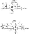
- FIG. 4 there is shown a typical prior art CMOS switch implementation.
- the leakage current (I Leak ) will happen during the phase detector hold period 306.
- V CC -V N .
- CSH capacitor
- This ⁇ V during lock can cause spurs at f out +/- 200 kHz as large as -20dBc (without the filter attenuation).
- the NMOS device 402 shown in FIG. 4 will not suffer because it's V GS is -V N and the leakage current is too low.
- the leakage current 404 problem can be much more severe than other issues associated with SH phase detectors including clock feedthrough and charge injection due to the CMOS switch.
- SH phase detectors used in frequency synthesizers sometimes also suffer from voltage glitches during lock.
- One reason for this problem is the leakage current of the sampling switch which results in charge leakage in the holding capacitor.
- the present invention describes a procedure which reduces the problem of leakage current in SH phase detectors.
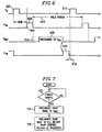
- the basic idea is to adjust the voltage (e.g., the V GS of the PMOS device 508 shown in FIG. 5 in the preferred embodiment) during the hold period 614 shown in FIG. 6, and just slightly before the ramp (ramp voltage signal V R ) starts 612.
- FIG. 5 An electrical model schematic of a proposed SH phase detector 500 in accordance with the invention is shown in FIG. 5, while the corresponding voltage waveforms are shown in FIG. 6.
- a precharge node e.g., node P in FIG. 4 shown in FIG. 5 as node P 502 is coupled to the input of the SH switch 504.
- V REF V REF ⁇ V CC
- the V GS of the PMOS switch 508 is positive and the leakage current is reduced drastically.
- the time between the rising edge 602 of the ramp voltage, V R 602, and the rising edge 604 of V SH is about 45 ns (nano-seconds).
- the pulse width 606 of V SH can be 5 ns.
- the voltage range at node N (V N ) 512 for the SH phase detector 500 is in the range of 0.5 V to V CC in this application. In one particular illustrative design, spurs were reduced 20-30 dB compared to the same SH phase detector that did not use the present invention's precharging technique.
- step 702 it is determined if a sample period has ended. If a sample period has ended, immediately or slightly thereafter, in step 704 the ramp node (node P 502) is charged to a first voltage level, which in this particular case is equal to V REF . In step 706, the ramp node is precharged to a second voltage level, which in this case is equal to V CC .
Landscapes
- Engineering & Computer Science (AREA)
- Power Engineering (AREA)
- Stabilization Of Oscillater, Synchronisation, Frequency Synthesizers (AREA)
- Manipulation Of Pulses (AREA)
- Gyroscopes (AREA)
- Analogue/Digital Conversion (AREA)
Abstract
Description
Claims (10)
- A method for reducing spurs in a sample and hold phase detector having a ramp node coupled to a sample and hold switch, which method comprising:(a) charging the ramp node to a first voltage level after a sample period has occurred; and(b) charging the ramp node to a second voltage level after step (a) .
- A method as defined in claim 1, wherein the step (b) comprises charging the ramp node to a second voltage level that is greater than said first voltage level.
- A method as defined in claim 1 or claim 2, further comprising the step of:(c) starting a new ramping period after step (b).
- A method as defined in any of claims 1 to 3, comprising performing steps (a) and (b) during the hold period of the sample and hold phase detector.
- A method as defined in claim 4, wherein step (a) comprises a longer duration than step (b).
- A method as defined in claim 5, comprising performing step (b) immediately after step (a) is completed.
- A sample and hold phase detector, comprising:a sample and hold switch coupled to a ramp node; andwherein the ramp node is arranged (a) to be charged to a first voltage level after a sample period has occurred; and (b) to be charged to a second voltage level after the ramp node has reached the first voltage level.
- A sample and hold phase detector as defined in claim 7, wherein the first voltage level is lower than the second voltage level.
- A method as defined in claim 7 or claim 8, wherein the sample and hold phase detector is arranged to initiate a new ramping period after the ramp node has reached the second voltage level.
- A method as defined in any of claims 7 to 9, wherein the ramp node is arranged to be charged to the first and second voltage levels during the hold period of the sample and hold phase detector.
Applications Claiming Priority (4)
| Application Number | Priority Date | Filing Date | Title |
|---|---|---|---|
| US22618400P | 2000-08-18 | 2000-08-18 | |
| US226184P | 2000-08-18 | ||
| US790377 | 2001-02-22 | ||
| US09/790,377 US6525521B2 (en) | 2000-08-18 | 2001-02-22 | Sample and hold phase detector having low spurious performance and method |
Publications (2)
| Publication Number | Publication Date |
|---|---|
| EP1184972A2 true EP1184972A2 (en) | 2002-03-06 |
| EP1184972A3 EP1184972A3 (en) | 2003-05-21 |
Family
ID=26920286
Family Applications (1)
| Application Number | Title | Priority Date | Filing Date |
|---|---|---|---|
| EP01000387A Withdrawn EP1184972A3 (en) | 2000-08-18 | 2001-08-17 | Phase Detector |
Country Status (3)
| Country | Link |
|---|---|
| US (1) | US6525521B2 (en) |
| EP (1) | EP1184972A3 (en) |
| JP (1) | JP2002111487A (en) |
Cited By (2)
| Publication number | Priority date | Publication date | Assignee | Title |
|---|---|---|---|---|
| US20070218362A1 (en) * | 2004-04-23 | 2007-09-20 | Akira Nagasaki | Lithium Ion Secondary Battery |
| US8223911B2 (en) | 2006-05-23 | 2012-07-17 | Deutsches Elektronen-Synchrotron Desy | Self-compensating drift-free high-frequency phase detector circuit |
Families Citing this family (4)
| Publication number | Priority date | Publication date | Assignee | Title |
|---|---|---|---|---|
| US7292407B2 (en) * | 2004-09-30 | 2007-11-06 | Hitachi Global Storage Technologies Netherlands B.V. | Disk drive with support structure for disk-vibration capacitive sensors |
| WO2006047268A1 (en) * | 2004-10-21 | 2006-05-04 | Massachusetts Institute Of Technology | Analog storage cell with low leakage |
| US7764759B2 (en) * | 2006-06-13 | 2010-07-27 | Gennum Corporation | Linear sample and hold phase detector for clocking circuits |
| US9742380B1 (en) * | 2016-06-01 | 2017-08-22 | Xilinx, Inc. | Phase-locked loop having sampling phase detector |
Family Cites Families (12)
| Publication number | Priority date | Publication date | Assignee | Title |
|---|---|---|---|---|
| US3646362A (en) | 1970-04-30 | 1972-02-29 | Rca Corp | Sample-and-hold circuit |
| JPS5549460B2 (en) * | 1974-01-18 | 1980-12-12 | ||
| US4216396A (en) | 1978-08-24 | 1980-08-05 | Rca Corporation | Sample-hold phase detector |
| NL7905541A (en) * | 1979-07-17 | 1981-01-20 | Philips Nv | PHASE CONNECTION. |
| US4361769A (en) * | 1980-07-01 | 1982-11-30 | Motorola, Inc. | Method for performing a sample and hold function |
| US4810904A (en) | 1985-07-17 | 1989-03-07 | Hughes Aircraft Company | Sample-and-hold phase detector circuit |
| CA1282465C (en) * | 1986-02-27 | 1991-04-02 | Hitachi, Ltd. | Phase-locked loop |
| US4864252A (en) * | 1988-09-26 | 1989-09-05 | Motorola, Inc. | Sample-and-hold phase detector for use in a phase locked loop |
| US5057793A (en) * | 1989-11-13 | 1991-10-15 | Cowley Nicholas P | Frequency synthesizer PLL having digital and analog phase detectors |
| DE4325680A1 (en) * | 1993-07-30 | 1995-02-02 | Acer Peripherals Inc | Device for detecting a signal frequency and for controlling a display device |
| US5483687A (en) * | 1993-11-10 | 1996-01-09 | Motorola, Inc. | Operational transconductance amplifier track and hold system |
| US5838180A (en) * | 1996-09-12 | 1998-11-17 | Lucent Technologies Inc. | Low-voltage frequency synthesizer |
-
2001
- 2001-02-22 US US09/790,377 patent/US6525521B2/en not_active Expired - Lifetime
- 2001-08-17 JP JP2001248084A patent/JP2002111487A/en not_active Withdrawn
- 2001-08-17 EP EP01000387A patent/EP1184972A3/en not_active Withdrawn
Cited By (2)
| Publication number | Priority date | Publication date | Assignee | Title |
|---|---|---|---|---|
| US20070218362A1 (en) * | 2004-04-23 | 2007-09-20 | Akira Nagasaki | Lithium Ion Secondary Battery |
| US8223911B2 (en) | 2006-05-23 | 2012-07-17 | Deutsches Elektronen-Synchrotron Desy | Self-compensating drift-free high-frequency phase detector circuit |
Also Published As
| Publication number | Publication date |
|---|---|
| EP1184972A3 (en) | 2003-05-21 |
| JP2002111487A (en) | 2002-04-12 |
| US6525521B2 (en) | 2003-02-25 |
| US20020039020A1 (en) | 2002-04-04 |
Similar Documents
| Publication | Publication Date | Title |
|---|---|---|
| US6369660B1 (en) | Circuit and method for preventing runaway in a phase lock loop | |
| EP0416840A2 (en) | Phase locked loop circuit with digital control | |
| US6392494B2 (en) | Frequency comparator and clock regenerating device using the same | |
| US7417479B2 (en) | Duty detection circuit and method for controlling the same | |
| KR100545947B1 (en) | Phase locked loop | |
| KR100423012B1 (en) | DLL with False Lock Protector | |
| US20120274362A1 (en) | Tracking and hold operations for an analog-to-digital converter | |
| CN101488710B (en) | A charge pump circuit | |
| US8531220B1 (en) | Loop filter | |
| CN101212225A (en) | Charge pump circuit and method capable of reducing current mismatch and phase-locked loop system | |
| GB1480355A (en) | Synchronizing circuits | |
| KR930011443A (en) | Linearized and delay-compensated all CMOS voltage controlled oscillators | |
| EP0238041B1 (en) | Phase locked loop circuit | |
| US20060197608A1 (en) | Fully programmable phase locked loop | |
| EP0287776B1 (en) | Phase-locked data detector | |
| US6525521B2 (en) | Sample and hold phase detector having low spurious performance and method | |
| CN110504958B (en) | Differential charge pump circuit with operational amplifier | |
| CN210469272U (en) | Phase-locked acceleration circuit and phase-locked loop system based on level width extraction | |
| US5459765A (en) | Phase comparator for biphase coded signal including preamble with code violation | |
| US4473760A (en) | Fast digital sample resolution circuit | |
| US4361769A (en) | Method for performing a sample and hold function | |
| CN112073059A (en) | DLL circuit | |
| US5589784A (en) | Method and apparatus for detecting changes in a clock signal to static states | |
| US7265636B2 (en) | Method of correcting the phase difference between two input signals of a phase-locked loop and associated device | |
| US4345219A (en) | Frequency agile hold-sample-hold phase detector |
Legal Events
| Date | Code | Title | Description |
|---|---|---|---|
| PUAI | Public reference made under article 153(3) epc to a published international application that has entered the european phase |
Free format text: ORIGINAL CODE: 0009012 |
|
| AK | Designated contracting states |
Kind code of ref document: A2 Designated state(s): AT BE CH CY DE DK ES FI FR GB GR IE IT LI LU MC NL PT SE TR |
|
| AX | Request for extension of the european patent |
Free format text: AL;LT;LV;MK;RO;SI |
|
| PUAL | Search report despatched |
Free format text: ORIGINAL CODE: 0009013 |
|
| AK | Designated contracting states |
Designated state(s): AT BE CH CY DE DK ES FI FR GB GR IE IT LI LU MC NL PT SE TR |
|
| AX | Request for extension of the european patent |
Extension state: AL LT LV MK RO SI |
|
| 17P | Request for examination filed |
Effective date: 20031015 |
|
| AKX | Designation fees paid |
Designated state(s): DE FR GB |
|
| RBV | Designated contracting states (corrected) |
Designated state(s): AT BE CH CY DE DK ES FI FR GB GR IE IT LI LU MC NL PT SE TR |
|
| 17Q | First examination report despatched |
Effective date: 20040325 |
|
| RBV | Designated contracting states (corrected) |
Designated state(s): DE FR GB |
|
| STAA | Information on the status of an ep patent application or granted ep patent |
Free format text: STATUS: THE APPLICATION IS DEEMED TO BE WITHDRAWN |
|
| 18D | Application deemed to be withdrawn |
Effective date: 20060330 |