EP1182712A2 - Method for forming high temperature superconducting Josephson junction - Google Patents
Method for forming high temperature superconducting Josephson junction Download PDFInfo
- Publication number
- EP1182712A2 EP1182712A2 EP01307108A EP01307108A EP1182712A2 EP 1182712 A2 EP1182712 A2 EP 1182712A2 EP 01307108 A EP01307108 A EP 01307108A EP 01307108 A EP01307108 A EP 01307108A EP 1182712 A2 EP1182712 A2 EP 1182712A2
- Authority
- EP
- European Patent Office
- Prior art keywords
- high temperature
- temperature superconducting
- josephson junction
- forming
- linear
- Prior art date
- Legal status (The legal status is an assumption and is not a legal conclusion. Google has not performed a legal analysis and makes no representation as to the accuracy of the status listed.)
- Granted
Links
Images

Classifications
-
- H—ELECTRICITY
- H10—SEMICONDUCTOR DEVICES; ELECTRIC SOLID-STATE DEVICES NOT OTHERWISE PROVIDED FOR
- H10N—ELECTRIC SOLID-STATE DEVICES NOT OTHERWISE PROVIDED FOR
- H10N60/00—Superconducting devices
- H10N60/01—Manufacture or treatment
- H10N60/0912—Manufacture or treatment of Josephson-effect devices
- H10N60/0941—Manufacture or treatment of Josephson-effect devices comprising high-Tc ceramic materials
Definitions
- the present invention relates to methods of forming high temperature superconducting Josephson junctions, more particularly, to a method of forming a high temperature superconducting Josephson junction which achieves a formation of a Josephson junction having high characteristics conveniently and quickly without necessitating costly micromachining facilities.
- a high temperature superconducting Josephson device has gained a high attention and has been required to be commercialized as a new electronic device which realizes, for example, an ultrahigh frequency generating device capable of generating frequencies in a range of terahertz or more, an ultrahigh frequency detecting device capable of detecting frequencies in a range of terahertz or more, a SQUID (superconducting quantum interference device) magnetometric sensor and, further, a digital device carrying a mass information processing system.
- an ultrahigh frequency generating device capable of generating frequencies in a range of terahertz or more
- an ultrahigh frequency detecting device capable of detecting frequencies in a range of terahertz or more
- a SQUID (superconducting quantum interference device) magnetometric sensor and, further, a digital device carrying a mass information processing system.
- the micromachining facilities which are used for producing a semiconductor device such as a convergence ion beam etching device and a photolithography device has ordinarily been employed.
- a problem in using the micromachining facilities for producing such devices that, for example, not only a tremendously high cost, but also a complexity of production process and an extended period of production time are necessary.
- the present invention has been accomplished under these circumstances and has an object to provide a method of forming a novel high temperature superconducting Josephson junction which achieves a formation of a Josephson junction having high characteristics conveniently and quickly without necessitating a costly micromachining facilities.
- the present invention provides, as a first aspect, a method of forming a high temperature superconducting Josephson junction comprising the steps of:
- the present invention provides a method of forming a high temperature superconducting Josephson junction comprising the steps of:
- the present invention provides a method of forming a high temperature superconducting Josephson junction comprising the steps of:
- the present invention provides the method of forming the high temperature superconducting Josephson junction of the above-described first aspect in which one or both of the high temperature superconducting whisker crystals are substituted by a linear high temperature superconducting monocrystal processed into an elongate linear shape.
- the present invention provides the method of forming the high temperature superconducting Josephson junction of the above-described third aspect in which the high temperature superconducting whisker crystal is substituted by a linear high temperature superconducting monocrystal processed into an elongate linear shape.
- the present invention provides the method of forming the high temperature superconducting Josephson junction of any one of the foregoing aspects in which the high temperature superconducting whisker crystal, the linear high temperature superconducting thin film or the linear high temperature superconducting monocrystal which is to form a Josephson junction is a compound containing at least one phase of Bismuth 2212 phase, Bismuth 2201 phase and Bismuth 2223 phase.
- the present invention provides the method of forming the high temperature superconducting Josephson junction of any one of the foregoing aspects in which the high temperature superconducting whisker crystal, the linear high temperature superconducting thin film or the linear high temperature superconducting monocrystal which is to form a Josephson junction turns mutual the c-face up, and forming a Josephson junction.
- the present invention provides the method of forming the high temperature superconducting Josephson junction of any one of the foregoing aspects in which the high temperature superconducting whisker crystal, the linear high temperature superconducting thin film or the linear high temperature superconducting monocrystal which is to form a Josephson junction are adjusted at 45 to 90 degrees in the cross angle, and forming a Josephson junction.
- the present invention provides the method of forming the high temperature superconducting Josephson junction of any one of the foregoing aspects in which the Josephson junction to be formed is an intrinsic Josephson junction.
- the present invention also provides a high temperature superconducting Josephson device provided with a Josephson junction to be formed by the method of forming the high temperature superconducting Josephson junction of any one of the foregoing aspects in which the high temperature superconducting Josephson device using other portions than a junction portion of a high temperature superconducting whisker crystal, a linear high temperature superconducting thin film or a linear high temperature superconducting monocrystal imparted with the Josephson junction as a wire material for a wire connection.
- the present invention has characteristics as described above; embodiments thereof will be described below.
- a Josephson junction having an extremely minute junction area is achieved by making use of a characteristic that a high temperature superconducting whisker crystal is in a needle like elongate shape. Specifically, for example, two high temperature superconducting whisker crystals are placed on a substrate such that they are crossed with each other and, then, subjected to thermal treatment to form a Josephson junction in a junction portion or in a neighborhood thereof. Since the junction area is extremely minute, it is not necessary to perform a special micromachining.
- About the temperature of thermal treatment making a maximum into the melting point of a sample to use and making a minimum into about 500 degrees C for example is illustrated as a general standard. More preferably, it is desirable to consider as 700 degrees C or more.
- a thermal treatment atmosphere it is desirable that oxygen is contained at least.
- a linear high temperature superconducting thin film mask-processed into an elongate linear shape may be used instead of using the high temperature superconducting whisker crystal.
- two linear high temperature superconducting thin films are placed on the substrate such that they are crossed with each other and then subjected to thermal treatment thereby forming a Josephson junction between the two linear high temperature superconducting thin layers.
- the high temperature superconducting whisker crystal and the linear high temperature superconducting thin film are placed each by one on the substrate such that they are crossed with each other and, then, subjected to thermal treatment to form the Josephson junction therebetween.
- the above-described whisker may be substituted by the linear high temperature superconducting monocrystal processed into an elongate linear shape.
- a Josephson junction can be formed from a bismuth system high temperature superconductor or the other high temperature superconductor by cutting down a single crystal long and slender and using it.
- the high temperature superconducting whisker crystal, the linear high temperature superconducting thin film or the linear high temperature superconducting monocrystal which is to form a Josephson junction may be various kinds of high temperature superconductors, preferably, is a compound which mainly contains either Bismuth 2212 phase, Bismuth 2201 phase and Bismuth 2223 phase. Moreover, it may be a compound containing at least two or more sorts of mixed phases of Bismuth 2212 phase, Bismuth 2201 phase and Bismuth 2223 phase.
- Examples of Josephson junctions to be formed by the method of forming the high temperature superconducting Josephson junction according to the present invention include an intrinsic Josephson junction. Ordinarily, it is extremely difficult to produce the intrinsic Josephson junction having a small number of junction layers; however, the method of forming the high temperature superconducting Josephson junction according to the present invention is capable of forming the intrinsic Josephson junction constituted with one layer or a small number of junction layers.
- the high temperature superconducting whisker crystal, the linear high temperature superconducting thin film or the linear high temperature superconducting monocrystal which is to form a Josephson junction can form a Josephson junction in arbitrary crystal faces mutually.
- a Josephson junction of the a-face and the a-face, a Josephson junction in the b-face and the b-face, etc. are possible.
- the optimum combination of a crystal face is the case where turns mutual the c-face up, and forming a Josephson junction. That is, it is joining the c-face.
- the Josephson characteristic is artificially controllable by changing a cross angle of these high temperature superconductors.
- Josephson current serves as the maximum, when for example, a cross angle is about 90 degrees, and it serves as the minimum at about 45 degrees. Therefore, in case Josephson junction is applied as an element, it is enabled to control artificially the timing (current value) of switching for every element.
- the high temperature superconducting Josephson device which has been provided with the Josephson junction formed by the method of forming the high temperature superconducting Josephson junction according to the present invention
- other portions than a junction portion of the high temperature superconducting whisker crystal, the linear high temperature superconducting thin film or the linear high temperature superconducting monocrystal which has been imparted with a Josephson junction are used as a wire material for a wire connection terminal whereby a wire connection in a superconducting state can be realized to materialize prevention of a malfunction caused by heat generation in the Josephson device and reduction of power consumption.
- the present invention has the characteristics as described above and will further be described in detail by reference to the non-limiting embodiments below.
- a Josephson junction was formed by a method of forming a high temperature superconducting Josephson junction according to the present invention.
- two Bismuth 2212 high temperature superconducting whiskers were placed on an MgO substrate such that they are crossed with each other to be in a cross shape. Subsequently, such two high temperature superconducting whiskers were placed in a furnace together with the substrate and subjected to thermal treatment under a condition that an oxygen atmosphere was controlled.
- sintering conditions a temperature was 850°C, an oxygen partial pressure was 70% and a period of time of sintering was 30 minutes.
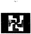
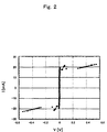
- FIG. 1 shows a photograph of a sample after subjected to thermal treatment. An end portion of the thus thermally treated sample was then provided with a current-voltage terminal. Current-voltage characteristics of a Josephson junction portion of the resultant sample were measured.
- FIG. 2 shows a result of the thus obtained measurements
- FIG. 3 shows a result of measurements of the current-voltage characteristics of the Josephson junction of the thus obtained sample. It is found from FIGS. 2 and 3 that advantageous superconducting characteristics have been obtained in each of the above-obtained samples.
- the present invention provides a method of forming a novel high temperature superconducting Josephson junction to achieve a formation of a Josephson junction having high characteristics conveniently and quickly without necessitating costly micromachining facilities.
- the present invention contributes to activation of research of a superconducting device and, further, with regard to the superconducting device, has a variety of technical effects such as reduction of production cost, simplification of production facilities and reduction of production time period.
- the Josephson device produced by the present invention is imparted with excellent functionality and characteristics; hence, capability of applications thereof to various fields such as communication technology, sensor technology and information processing technology can be considered and are strongly required to be commercialized.
Landscapes
- Engineering & Computer Science (AREA)
- Chemical & Material Sciences (AREA)
- Ceramic Engineering (AREA)
- Manufacturing & Machinery (AREA)
- Superconductor Devices And Manufacturing Methods Thereof (AREA)
Abstract
Description
For example, a Josephson junction of the a-face and the a-face, a Josephson junction in the b-face and the b-face, etc. are possible. And The optimum combination of a crystal face is the case where turns mutual the c-face up, and forming a Josephson junction. That is, it is joining the c-face. Moreover, the Josephson characteristic is artificially controllable by changing a cross angle of these high temperature superconductors. Specifically, Josephson current serves as the maximum, when for example, a cross angle is about 90 degrees, and it serves as the minimum at about 45 degrees. Therefore, in case Josephson junction is applied as an element, it is enabled to control artificially the timing (current value) of switching for every element.
Claims (10)
- A method of forming a high temperature superconducting Josephson junction comprising the steps of:crossing high temperature superconducting whisker crystals with each other;subjecting the thus crossed high temperature superconducting whisker crystals to thermal treatment; andforming a Josephson junction in a combined portion of the high temperature superconducting whisker crystals or in a neighborhood of said combined portion.
- A method of forming a high temperature superconducting Josephson junction comprising the steps of:crossing linear high temperature superconducting thin films mask-processed into an elongate linear shape with each other;subjecting the thus crossed linear high temperature superconducting thin films mask-processed into an elongate linear shape to thermal treatment; andforming a Josephson junction between the linear high temperature superconducting thin films.
- A method of forming a high temperature superconducting Josephson junction comprising the steps of:crossing a linear high temperature superconducting thin film mask-processed into an elongate linear shape and a high temperature superconducting whisker crystal;subjecting the thus crossed linear high temperature superconducting thin film mask-processed into an elongate linear shape and high temperature superconducting whisker crystal to thermal treatment; andforming a Josephson junction between the linear high temperature superconducting thin film and the high temperature superconducting whisker crystal.
- The method of forming the high temperature superconducting Josephson junction as set forth in Claim 1, wherein one or both of the high temperature superconducting whisker crystals are substituted by a linear high temperature superconducting monocrystal processed into an elongate linear shape.
- The method of forming the high temperature superconducting Josephson junction as set forth in Claim 3, wherein the high temperature superconducting whisker crystal is substituted by a linear high temperature superconducting monocrystal processed into an elongate linear shape.
- The method of forming the high temperature superconducting Josephson junction as set forth in any one of Claims 1 to 5, wherein the high temperature superconducting whisker crystal, the linear high temperature superconducting thin film or the linear high temperature superconducting monocrystal which is to form a Josephson junction is a compound containing at least one phase of Bismuth 2212 phase, Bismuth 2201 phase and Bismuth 2223 phase.
- The method of forming the high temperature superconducting Josephson junction as set forth in any one of Claims 1 to 6, wherein the high temperature superconducting whisker crystal, the linear high temperature superconducting thin film or the linear high temperature superconducting monocrystal which is to form a Josephson junction turns mutual the c-face up, and forming a Josephson junction.
- The method of forming the high temperature superconducting Josephson junction as set forth in any one of Claims 1 to 7, wherein the high temperature superconducting whisker crystal, the linear high temperature superconducting thin film or the linear high temperature superconducting monocrystal which is to form a Josephson junction are adjusted at 45 to 90 degrees in the cross angle, and forming a Josephson junction.
- The method of forming the high temperature superconducting Josephson junction as set forth in any one of Claims 1 to 6, wherein the Josephson junction to be formed is an intrinsic Josephson junction.
- A high temperature superconducting Josephson device provided with a Josephson junction to be formed by the method of forming the high temperature superconducting Josephson junction as set forth in any one of Claims 1 to 7, the high temperature superconducting Josephson device using other portions than a junction portion of a high temperature superconducting whisker crystal, a linear high temperature superconducting thin film or a linear high temperature superconducting monocrystal imparted with the Josephson junction as a wire material for a wire connection.
Applications Claiming Priority (2)
| Application Number | Priority Date | Filing Date | Title |
|---|---|---|---|
| JP2000250269 | 2000-08-21 | ||
| JP2000250269 | 2000-08-21 |
Publications (3)
| Publication Number | Publication Date |
|---|---|
| EP1182712A2 true EP1182712A2 (en) | 2002-02-27 |
| EP1182712A3 EP1182712A3 (en) | 2004-10-06 |
| EP1182712B1 EP1182712B1 (en) | 2008-07-23 |
Family
ID=18739875
Family Applications (1)
| Application Number | Title | Priority Date | Filing Date |
|---|---|---|---|
| EP01307108A Expired - Lifetime EP1182712B1 (en) | 2000-08-21 | 2001-08-21 | Method for forming high temperature superconducting Josephson junction |
Country Status (3)
| Country | Link |
|---|---|
| US (2) | US6682621B2 (en) |
| EP (1) | EP1182712B1 (en) |
| DE (1) | DE60134923D1 (en) |
Cited By (1)
| Publication number | Priority date | Publication date | Assignee | Title |
|---|---|---|---|---|
| EP1548853A4 (en) * | 2002-09-20 | 2007-03-28 | Nat Inst For Materials Science | JUNCTION TUNNEL JOSEPHSON OF HIGH TEMPERATURE SUPERCONDUCTOR |
Families Citing this family (3)
| Publication number | Priority date | Publication date | Assignee | Title |
|---|---|---|---|---|
| US20060138948A1 (en) * | 2004-12-27 | 2006-06-29 | Quantum Paper, Inc. | Addressable and printable emissive display |
| JP2008140769A (en) * | 2006-11-06 | 2008-06-19 | Sumitomo Electric Ind Ltd | Production method of Bi2223 superconducting wire |
| EP4270504A1 (en) * | 2022-04-26 | 2023-11-01 | Terra Quantum AG | Contact layer for layered materials |
Family Cites Families (14)
| Publication number | Priority date | Publication date | Assignee | Title |
|---|---|---|---|---|
| US3706064A (en) * | 1971-05-07 | 1972-12-12 | Bell Telephone Labor Inc | Magnetically controlled supercurrent switch |
| US4157555A (en) * | 1977-11-07 | 1979-06-05 | The United States Of America As Represented By The United States Department Of Energy | Superconducting transistor |
| US4494131A (en) * | 1980-10-31 | 1985-01-15 | Rikagaku Kenkyusho | Josephson junction element and method of making the same |
| JPS5846197B2 (en) * | 1980-12-20 | 1983-10-14 | 理化学研究所 | Josephson junction device and its manufacturing method |
| JPS61181178A (en) * | 1985-02-06 | 1986-08-13 | Rikagaku Kenkyusho | Josephson junction element and manufacture thereof |
| US4904882A (en) * | 1988-09-30 | 1990-02-27 | The United States Of America As Represented By The Secretary Of The Navy | Superconducting optical switch |
| JP2746990B2 (en) * | 1989-03-16 | 1998-05-06 | 株式会社東芝 | Superconducting element |
| JPH03270280A (en) * | 1990-03-09 | 1991-12-02 | Univ California | Microelectron circuit element having superconductive crosspath and manu- facture thereof |
| JPH04338684A (en) * | 1991-05-16 | 1992-11-25 | Nec Corp | Josephson element and its manufacturing method |
| JP3189403B2 (en) * | 1991-07-16 | 2001-07-16 | 住友電気工業株式会社 | Element having superconducting junction and method of manufacturing the same |
| JPH05190927A (en) * | 1992-01-16 | 1993-07-30 | Nec Corp | Tunnel type josephson junction element and its manufacture |
| JP3319205B2 (en) * | 1995-02-28 | 2002-08-26 | 株式会社島津製作所 | Method of manufacturing Josephson junction device |
| JPH09121064A (en) * | 1995-10-26 | 1997-05-06 | Fujitsu Ltd | High temperature superconducting Josephson junction device |
| JP4033997B2 (en) * | 1999-01-26 | 2008-01-16 | 独立行政法人科学技術振興機構 | Electronic element manufacturing method and manufacturing apparatus using workable material capable of anisotropic etching |
-
2001
- 2001-08-21 DE DE60134923T patent/DE60134923D1/en not_active Expired - Lifetime
- 2001-08-21 EP EP01307108A patent/EP1182712B1/en not_active Expired - Lifetime
- 2001-08-21 US US09/932,941 patent/US6682621B2/en not_active Expired - Fee Related
-
2003
- 2003-06-09 US US10/456,703 patent/US6839578B2/en not_active Expired - Fee Related
Cited By (1)
| Publication number | Priority date | Publication date | Assignee | Title |
|---|---|---|---|---|
| EP1548853A4 (en) * | 2002-09-20 | 2007-03-28 | Nat Inst For Materials Science | JUNCTION TUNNEL JOSEPHSON OF HIGH TEMPERATURE SUPERCONDUCTOR |
Also Published As
| Publication number | Publication date |
|---|---|
| EP1182712A3 (en) | 2004-10-06 |
| US6839578B2 (en) | 2005-01-04 |
| US20020025586A1 (en) | 2002-02-28 |
| US20030211946A1 (en) | 2003-11-13 |
| US6682621B2 (en) | 2004-01-27 |
| EP1182712B1 (en) | 2008-07-23 |
| DE60134923D1 (en) | 2008-09-04 |
Similar Documents
| Publication | Publication Date | Title |
|---|---|---|
| JP2907832B2 (en) | Superconducting device and manufacturing method thereof | |
| Flukiger et al. | High critical current densities in Bi (2223)/Ag tapes | |
| US5278140A (en) | Method for forming grain boundary junction devices using high Tc superconductors | |
| Fujishita et al. | Comparison of the normal state properties between the superconducting and the nonsuperconducting metallic phases in La2− ySryCu− xNixO4 | |
| US6682621B2 (en) | Method of forming high temperature superconducting josephson junction | |
| Takano et al. | A cross-whiskers junction as a novel fabrication process for intrinsic Josephson junctions | |
| Reddy et al. | Mono-domain YBa2Cu3O y superconductor fabrics prepared by an infiltration process | |
| JP3189403B2 (en) | Element having superconducting junction and method of manufacturing the same | |
| JP3890415B2 (en) | SQUID magnetic sensor and method for manufacturing SQUID magnetic sensor | |
| EP0650203B1 (en) | Oxide superconductor and process of producing the same | |
| JP3379533B2 (en) | Method for manufacturing superconducting device | |
| Stepantsov et al. | On the possibility of usage of crystalline composites in investigations of high-T c superconductivity | |
| US6482775B2 (en) | Oxide superconductor | |
| JP2698858B2 (en) | Method for forming oxide superconductor | |
| JP2002141566A (en) | High-Tc superconducting Josephson junction formation method | |
| Wellhofer et al. | The effect of lead doping and grain alignment on Bi-Sr-Ca-Cu-O superconductors | |
| JP2519337B2 (en) | Substrate material for producing oxide superconductor and method for producing oxide superconductor | |
| Xiaowen et al. | A high Tc proximity effect superconductor and its superconductivity | |
| JP2004111864A (en) | High temperature superconducting Josephson tunnel junction | |
| JPH03275504A (en) | Oxide superconductor thin film and its production | |
| Phillips | High-temperature superconducting thin films | |
| JPH0227612A (en) | Oxide superconducting wire | |
| JPH0195576A (en) | Method for manufacturing thin film superconducting elements | |
| JPH0738165A (en) | Superconducting Josephson device fabrication method | |
| JP2002220230A (en) | Quantum defect magnetic flux pinned superconducting material and method of manufacturing the same |
Legal Events
| Date | Code | Title | Description |
|---|---|---|---|
| PUAI | Public reference made under article 153(3) epc to a published international application that has entered the european phase |
Free format text: ORIGINAL CODE: 0009012 |
|
| AK | Designated contracting states |
Kind code of ref document: A2 Designated state(s): AT BE CH CY DE DK ES FI FR GB GR IE IT LI LU MC NL PT SE TR |
|
| AX | Request for extension of the european patent |
Free format text: AL;LT;LV;MK;RO;SI |
|
| PUAL | Search report despatched |
Free format text: ORIGINAL CODE: 0009013 |
|
| AK | Designated contracting states |
Kind code of ref document: A3 Designated state(s): AT BE CH CY DE DK ES FI FR GB GR IE IT LI LU MC NL PT SE TR |
|
| AX | Request for extension of the european patent |
Extension state: AL LT LV MK RO SI |
|
| 17P | Request for examination filed |
Effective date: 20050107 |
|
| 17Q | First examination report despatched |
Effective date: 20050215 |
|
| AKX | Designation fees paid |
Designated state(s): CH DE FR GB LI |
|
| GRAP | Despatch of communication of intention to grant a patent |
Free format text: ORIGINAL CODE: EPIDOSNIGR1 |
|
| GRAS | Grant fee paid |
Free format text: ORIGINAL CODE: EPIDOSNIGR3 |
|
| GRAA | (expected) grant |
Free format text: ORIGINAL CODE: 0009210 |
|
| AK | Designated contracting states |
Kind code of ref document: B1 Designated state(s): CH DE FR GB LI |
|
| REG | Reference to a national code |
Ref country code: GB Ref legal event code: FG4D |
|
| REG | Reference to a national code |
Ref country code: CH Ref legal event code: EP Ref country code: CH Ref legal event code: NV Representative=s name: BOHEST AG |
|
| REF | Corresponds to: |
Ref document number: 60134923 Country of ref document: DE Date of ref document: 20080904 Kind code of ref document: P |
|
| PLBE | No opposition filed within time limit |
Free format text: ORIGINAL CODE: 0009261 |
|
| STAA | Information on the status of an ep patent application or granted ep patent |
Free format text: STATUS: NO OPPOSITION FILED WITHIN TIME LIMIT |
|
| 26N | No opposition filed |
Effective date: 20090424 |
|
| REG | Reference to a national code |
Ref country code: CH Ref legal event code: PCAR Free format text: NEW ADDRESS: HOLBEINSTRASSE 36-38, 4051 BASEL (CH) |
|
| PGFP | Annual fee paid to national office [announced via postgrant information from national office to epo] |
Ref country code: CH Payment date: 20140820 Year of fee payment: 14 Ref country code: DE Payment date: 20140821 Year of fee payment: 14 |
|
| PGFP | Annual fee paid to national office [announced via postgrant information from national office to epo] |
Ref country code: GB Payment date: 20140820 Year of fee payment: 14 Ref country code: FR Payment date: 20140821 Year of fee payment: 14 |
|
| REG | Reference to a national code |
Ref country code: DE Ref legal event code: R119 Ref document number: 60134923 Country of ref document: DE |
|
| REG | Reference to a national code |
Ref country code: CH Ref legal event code: PL |
|
| GBPC | Gb: european patent ceased through non-payment of renewal fee |
Effective date: 20150821 |
|
| PG25 | Lapsed in a contracting state [announced via postgrant information from national office to epo] |
Ref country code: LI Free format text: LAPSE BECAUSE OF NON-PAYMENT OF DUE FEES Effective date: 20150831 Ref country code: CH Free format text: LAPSE BECAUSE OF NON-PAYMENT OF DUE FEES Effective date: 20150831 |
|
| REG | Reference to a national code |
Ref country code: FR Ref legal event code: ST Effective date: 20160429 |
|
| PG25 | Lapsed in a contracting state [announced via postgrant information from national office to epo] |
Ref country code: GB Free format text: LAPSE BECAUSE OF NON-PAYMENT OF DUE FEES Effective date: 20150821 Ref country code: DE Free format text: LAPSE BECAUSE OF NON-PAYMENT OF DUE FEES Effective date: 20160301 |
|
| PG25 | Lapsed in a contracting state [announced via postgrant information from national office to epo] |
Ref country code: FR Free format text: LAPSE BECAUSE OF NON-PAYMENT OF DUE FEES Effective date: 20150831 |