EP1179739A1 - Procédé pour tester un circuit intégré à contrôle de cadencement flexible - Google Patents
Procédé pour tester un circuit intégré à contrôle de cadencement flexible Download PDFInfo
- Publication number
- EP1179739A1 EP1179739A1 EP01202908A EP01202908A EP1179739A1 EP 1179739 A1 EP1179739 A1 EP 1179739A1 EP 01202908 A EP01202908 A EP 01202908A EP 01202908 A EP01202908 A EP 01202908A EP 1179739 A1 EP1179739 A1 EP 1179739A1
- Authority
- EP
- European Patent Office
- Prior art keywords
- clock
- heart
- core
- clock input
- inhibition
- Prior art date
- Legal status (The legal status is an assumption and is not a legal conclusion. Google has not performed a legal analysis and makes no representation as to the accuracy of the status listed.)
- Withdrawn
Links
Images


Classifications
-
- G—PHYSICS
- G01—MEASURING; TESTING
- G01R—MEASURING ELECTRIC VARIABLES; MEASURING MAGNETIC VARIABLES
- G01R31/00—Arrangements for testing electric properties; Arrangements for locating electric faults; Arrangements for electrical testing characterised by what is being tested not provided for elsewhere
- G01R31/28—Testing of electronic circuits, e.g. by signal tracer
- G01R31/317—Testing of digital circuits
- G01R31/3181—Functional testing
- G01R31/3185—Reconfiguring for testing, e.g. LSSD, partitioning
- G01R31/318533—Reconfiguring for testing, e.g. LSSD, partitioning using scanning techniques, e.g. LSSD, Boundary Scan, JTAG
- G01R31/318552—Clock circuits details
Definitions
- the present invention relates to a method for testing an integrated circuit including a core and a plurality of memory cells having outputs and inputs alternately connected to inputs and outputs of the heart, the heart being provided with a clock input for receiving a first clock signal in operating mode normal, each memory cell being identified by an address and provided with an input for receiving a second clock signal in test mode, the clock input of the heart being subject to conditional inhibition in test mode.
- the number of clock pulses required to emulate an operating sequence varies from one sequence to another. Thus, it will be necessary to assign to the clock register a large size to adapt it to long operating sequences, which will require a large number of clock pulses.
- the size of the clock register is of the order of 50% of that of the control register.
- the dimensions of the clock register being definitively fixed during the design of the integrated circuit, it will be necessary to use a large silicon surface to carry out the function of memorizing the number of clock pulses in test mode.
- an up / down counting device must be used in order to control the number of clock pulses sent to the core, which further increases the surface area of the integrated circuit implementing the known method.
- the invention aims to remedy these drawbacks by proposing a method to test an integrated circuit whereby the delivery of clock pulses to the heart in test mode is carried out in a simple and flexible way, without requiring programming, within a specific register, a number of pulses specific to each operating sequence.
- the simple selection of a virtual address gives rise to the transmission of a clock pulse to the clock input of the heart. N successive selections a virtual address will send a train of N clock pulses to the core. he it is therefore no longer necessary to pre-program this number N in a register, which gives the process according to the invention great flexibility of use, which results in savings in terms of silicon surface area and production cost of the integrated circuit.
- the clock input of the heart receives second clock signal when inhibition of said clock input is lifted during test mode.
- Such an implementation makes it possible to clock the integrated circuit by means of the only second clock signal for the duration of the test mode, which avoids clock switches which are always difficult to manage.
- the lifting of the inhibition of the clock input of the heart is also subject to the execution of an operation relating to the virtual address.
- the selection of a virtual address announces the lifting the inhibition of the clock input, the duration of this lifting of inhibition, and therefore the number of clock pulses transmitted to the heart, being determined by the number of operations relating to said virtual address which will be executed.
- the lifting of inhibiting the clock input of the heart is further subject to the execution of an operation specific predetermined relating to the virtual address.
- the specific operation predetermined is an offset operation.
- control module is configured to route the second clock signal to the heart clock input when inhibition of said input is lifted during test mode.
- the lifting of the inhibition of the clock input of the heart during the test mode is furthermore subject to the execution of a operation relating to the virtual address.
- the detection signal Shdv will be activated by the DBUG machine when it has ordered either a selection of a virtual address or an operation, by example an offset, relative to such an address.
- the CORE core clock input is a priori inhibited in test mode, the CORE core is at rest.
- test of a given operating sequence generally takes place in three stages:
- the DBUG machine In a first phase, called loading, the DBUG machine writes to the CR control of information representing stimuli to be applied to the CORE heart in order to emulate a specific operating sequence.
- a loading is clocked by means of the second clock signal Clk2, by ordering as many shifts of the content of the register observation as necessary by means of an offset signal S simultaneously applied to all the memory cells forming the observation register OR.
- a clock pulse is transmitted to the heart whenever an offset operation is controlled by the DBUG machine in relation to a virtual address which does not correspond to no memory cells. Such an event is identified by an active state of the detection signal Shdv transmitted by the TPORT serial port to the CNT control module.
- a third phase the value of the content of the observation register OR is compared by the DBUG machine with a numerical reference value, representative of the CORE heart's response to the stimuli it received. In case of identity between these values, it will be concluded that the CORE core has correctly executed the operating sequence chosen.
- the roles of the CR and OR control and observation registers will be reversed. Indeed, if one wishes to test a peripheral not shown in the figure, by example a block of RAM memory, it is the observation register OR which will contain stimuli simulating commands from the CORE core, in response to which the device will deliver signals towards the CORE core, signals which will then be memorized by the CR control register for validation by the DBUG machine.
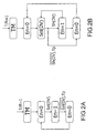
- FIG. 2A represents the sequence of an inhibition / inhibition lifting sequence implemented by the control module according to the invention.
- the integrated circuit is configured in test mode during a first step TM by means of the T / R signal which then takes an active state, here logic level 1.
- each Sel (DV) selection of a virtual DV address causes the transmission of a clock pulse to the heart.
- FIG. 2B represents the sequence of an inhibition / inhibition lifting sequence implemented by the control module according to a variant of the invention.
- the integrated circuit is configured in test mode during a first step TM by means of the T / R signal which then takes an active state, here the logic level 1.
- the clock input of the heart is immediately inhibited by putting an signal, here logic level 0, of a signal authorization In.
- each shift Sh (DV) operation relating to a virtual address DV causes the transmission of a clock pulse to the heart.
- This variant of the invention takes full advantage of the format of the sequences in accordance with JTAG standard (for Joint Test Action Group), according to which the selection of an address must be followed by one or more shift operations relating to this address.
- JTAG standard for Joint Test Action Group
- a DBUG machine conforming to the JTAG standard can therefore easily software control the supply of pulses to the heart during the emulation phase without that it is necessary to modify the said machine for this purpose.
- FIG. 3 schematically represents a possible embodiment of the module CNT control.
- the CNT control module includes an ET AG gate, one of which output will be connected to the clock input of the heart in order to provide it with a clock signal Clkin, gate ET AG of which an input will receive a clock signal Clk and of which another input will receive the authorization signal En.
- An inactive state of said signal En that is to say in this example a logic level 0, will command therefore inhibition of the clock input of the heart, and an active state of the authorization signal En, that is to say in this example a logic level 1, will command an input inhibition lift heart clock.
- the CNT control module also includes a DL memory cell, produced here by means of a flip-flop D, of which a data input D will receive the detection signal Shdv, of which an output data Q will issue the authorization signal En, and one clock input of which will receive the inverse of the clock signal Clk.
- the CNT control module also includes an MC multiplexer for selecting, means of the control signal T / R in this example, that of the first and second signals clock Clk1 and Clk2 which must constitute the clock signal Clk whose active edges will be transmitted to the heart.
- the heart will receive the first clock signal Clk1 when the T / R control signal will be inactive, i.e. at logic level 0, in normal operation, and the second clock signal Clk2 when the control signal T / R will be active, i.e. at logic level 1, in test mode, provided that the signal authorization is also active.
- FIG. 4 represents the evolution of signals present in the control module described above.
- the En authorization signal is inactive and the heart clock input is inhibited.
- the detection signal Shdv is activated, and remains active until time t2.
- This active state representative of a selection of a virtual address or of an operation relating to such a address, according to the mode of implementation of the invention chosen, is memorized by the flip-flop D DL at an instant t2 corresponding to the falling edge of the clock signal Clk which follows the instant t1.
- the authorization signal En is then activated and causes the input inhibition to be lifted heart clock.
- a deactivation of the detection signal Shdv occurring at an instant according to t3 has no influence on the authorization signal En.
- the authorization signal will remain active at least until time t4 corresponding to the next falling edge of the signal clock Clk, that is to say during a duration Tp equal to a period of said signal Clk. During of this period, the clock signal Clk will have presented an active edge, in this case at the instant t3, which will have been transmitted to the heart by the Clkin signal. At time t4, the detection signal Shdv not having been reactivated, the authorization signal En is deactivated and the clock input of the heart is inhibited again. It is clear from this sequence that when selecting an address virtual or an operation relating to such an address, depending on the implementation mode of the invention chosen, corresponds to the transmission of a clock pulse to the heart.
- the detection signal Shdv is reactivated, causing an activation of the signal authorization En at a time t6 corresponding to the falling edge of the clock signal Clk which follows time t5.
- the detection signal Shdv is successively reactivated at instants consecutive t7 and t8, and deactivated at an instant t9.
- This scenario illustrates three selections successive virtual address, or three successive operations relating to a virtual address, according to the mode of implementation of the invention chosen.
- the authorization signal En is thus activated during three successive periods of the clock signal Clk, allowing, due to the lifting of the inhibition which it commands, to transmit to the heart three clock pulses by the signal Clkin.
- the detection signal Shdv not having been reactivated the signal En authorization is disabled and the heart clock input is inhibited again. It comes out clearly from this sequence that at N successive selections of a virtual address or N successive operations relating to such an address, according to the mode of implementation of the invention chosen, corresponds to the transmission of N clock pulses to the heart.
- the invention thus makes it possible to route clock pulses in test mode so simple and flexible, without any prior programming of the number of pulses specific to the the tested operating sequence is not necessary.
Landscapes
- Engineering & Computer Science (AREA)
- General Engineering & Computer Science (AREA)
- Physics & Mathematics (AREA)
- General Physics & Mathematics (AREA)
- Tests Of Electronic Circuits (AREA)
- Test And Diagnosis Of Digital Computers (AREA)
Abstract
Description
Lorsque le circuit intégré est en mode test, l'entrée d'horloge du coeur est à priori inhibée et le coeur est au repos.
Le test d'une séquence opératoire donnée se déroule généralement en trois temps :
Dans le procédé connu, la taille du registre d'horloge est de l'ordre de 50% de celle du registre de contrôle. Ces registres étant chargés bit par bit selon un mode série, l'utilisation d'un registre d'horloge pour générer des impulsions d'horloge en mode test augmente la durée de la phase de chargement de 50%, et celle de la totalité du test d'une séquence opératoire de 30 à 50%, selon la durée de la phase d'émulation et la taille du registre d'observation. Une telle augmentation de la durée du test selon le procédé connu diminue le débit de production et augmente de manière significative le coût total de production du circuit intégré.
Par ailleurs, un dispositif de comptage/décomptage doit être utilisé afin de contrôler le nombre d'impulsions d'horloge envoyées au coeur, ce qui augmente encore la surface du circuit intégré mettant en oeuvre le procédé connu.
- configuration du circuit en mode test,
- sélection d'une adresse dite virtuelle ne correspondant à aucune cellule mémoire,
- levée de l'inhibition de l'entrée d'horloge du coeur pendant une durée prédéterminée consécutive à ladite sélection.
- un coeur muni d'une entrée d'horloge destinée à recevoir un premier signal d'horloge en mode de fonctionnement normal,
- une pluralité de cellules mémoire présentant des sorties et des entrées alternativement connectées à des entrées et à des sorties du coeur, chaque cellule mémoire étant identifiée par une adresse et munie d'une entrée d'horloge destinée à recevoir un deuxième signal d'horloge en mode test,
- un module de contrôle destiné à réaliser une inhibition de l'entrée d'horloge du coeur en mode test, agencés de manière à ce que ladite inhibition soit levée pendant une durée prédéterminée, après qu'une adresse virtuelle ne correspondant à aucune cellule mémoire ait été sélectionnée.
- la figure 1 est un schéma fonctionnel décrivant un circuit intégré conforme à un mode de réalisation de l'invention,
- les figures 2A et 2B sont des organigrammes représentant le déroulement de séquences d'inhibition/levée d'inhibition incluses dans des procédés conformes à l'invention et à l'une de ses variantes, respectivement,
- la figure 3 est schéma fonctionnel représentant un module d'inhibition conditionnelle de l'entrée d'horloge du coeur, et
- la figure 4 est un ensemble de chronogrammes représentant l'évolution de signaux présents dans un tel module.
- un coeur CORE muni d'une entrée d'horloge destinée à recevoir un premier signal d'horloge Clk1 en mode de fonctionnement normal,
- une pluralité de cellules mémoire DIi (pour i=1 à N) et DOj (pour j=1 à P) présentant des sorties Q et des entrées D alternativement connectées à des entrées INi (pour i=1 à N) et à des sorties OUTj (pour j=1 à P) du coeur CORE via des multiplexeurs MIi (pour i=1 à N) et MOj (pour j=1 à P), chaque cellule mémoire étant identifiée par une adresse et munie d'une entrée d'horloge destinée à recevoir un deuxième signal d'horloge Clk2 en mode test,
- un module de contrôle CNT destiné à réaliser une inhibition de l'entrée d'horloge du coeur CORE en mode test, agencé de manière à ce que ladite inhibition soit levée pendant une durée prédéterminée après qu'un signal de détection Shdv aura été activé.
Claims (8)
- Procédé pour tester un circuit intégré incluant un coeur et une pluralité de cellules mémoire présentant des sorties et des entrées alternativement connectées à des entrées et à des sorties du coeur, le coeur étant muni d'une entrée d'horloge destinée à recevoir un premier signal d'horloge en mode de fonctionnement normal, chaque cellule mémoire étant identifiée par une adresse et munie d'une entrée d'horloge destinée à recevoir un deuxième signal d'horloge en mode test, l'entrée d'horloge du coeur étant soumise à une inhibition conditionnelle en mode test, procédé incluant les étapes suivantes :configuration du circuit en mode test,sélection d'une adresse dite virtuelle ne correspondant à aucune cellule mémoire,levée de l'inhibition de l'entrée d'horloge du coeur pendant une durée prédéterminée consécutive à ladite sélection.
- Procédé conforme à la revendication 1, selon lequel l'entrée d'horloge du coeur reçoit le deuxième signal d'horloge lorsque l'inhibition de ladite entrée d'horloge est levée pendant le mode test.
- Procédé conforme à la revendication 1, selon lequel la levée de l'inhibition de l'entrée d'horloge du coeur est en outre assujettie à l'exécution d'une opération relative à l'adresse virtuelle.
- Procédé conforme à la revendication 1, selon lequel la levée de l'inhibition de l'entrée d'horloge du coeur est en outre assujettie à l'exécution d'une opération spécifique prédéterminée relative à l'adresse virtuelle.
- Procédé conforme à la revendication 4, selon lequel l'opération spécifique prédéterminée est une opération de décalage.
- Circuit intégré incluant :un coeur muni d'une entrée d'horloge destinée à recevoir un premier signal d'horloge en mode de fonctionnement normal,une pluralité de cellules mémoire présentant des sorties et des entrées alternativement connectées à des entrées et à des sorties du coeur, chaque cellule mémoire étant identifiée par une adresse et munie d'une entrée d'horloge destinée à recevoir un deuxième signal d'horloge en mode test,un module de contrôle destiné à réaliser une inhibition de l'entrée d'horloge du coeur en mode test, agencé de manière à ce que ladite inhibition soit levée pendant une durée prédéterminée après qu'une adresse virtuelle ne correspondant à aucune cellule mémoire ait été sélectionnée.
- Circuit intégré conforme à la revendication 6, dans lequel le module de contrôle est configuré pour acheminer le deuxième signal d'horloge vers l'entrée d'horloge du coeur lorsque l'inhibition de ladite entrée est levée pendant le mode test.
- Circuit intégré conforme à la revendication 6, dans lequel la levée de l'inhibition de l'entrée d'horloge du coeur pendant le mode test est en outre assujettie à l'exécution d'une opération relative à l'adresse virtuelle.
Applications Claiming Priority (2)
| Application Number | Priority Date | Filing Date | Title |
|---|---|---|---|
| FR0010441 | 2000-08-08 | ||
| FR0010441A FR2812948A1 (fr) | 2000-08-08 | 2000-08-08 | Procede pour tester un circuit integre a controle de cadencement flexible |
Publications (1)
| Publication Number | Publication Date |
|---|---|
| EP1179739A1 true EP1179739A1 (fr) | 2002-02-13 |
Family
ID=8853406
Family Applications (1)
| Application Number | Title | Priority Date | Filing Date |
|---|---|---|---|
| EP01202908A Withdrawn EP1179739A1 (fr) | 2000-08-08 | 2001-07-31 | Procédé pour tester un circuit intégré à contrôle de cadencement flexible |
Country Status (4)
| Country | Link |
|---|---|
| US (1) | US6775797B2 (fr) |
| EP (1) | EP1179739A1 (fr) |
| JP (1) | JP2002156423A (fr) |
| FR (1) | FR2812948A1 (fr) |
Families Citing this family (6)
| Publication number | Priority date | Publication date | Assignee | Title |
|---|---|---|---|---|
| US6848068B1 (en) * | 2000-06-07 | 2005-01-25 | Cypress Semiconductor Corp. | Soft coding of multiple device IDs for IEEE compliant JTAG devices |
| JP4179827B2 (ja) * | 2002-08-30 | 2008-11-12 | Necエレクトロニクス株式会社 | メモリのテスト回路 |
| JP2005243759A (ja) * | 2004-02-25 | 2005-09-08 | Oki Electric Ind Co Ltd | 半導体装置及び半導体装置の評価方法 |
| US7818640B1 (en) | 2004-10-22 | 2010-10-19 | Cypress Semiconductor Corporation | Test system having a master/slave JTAG controller |
| US20060168490A1 (en) * | 2005-01-24 | 2006-07-27 | Mccormack James A | Apparatus and method of controlling test modes of a scannable latch in a test scan chain |
| US8310885B2 (en) | 2010-04-28 | 2012-11-13 | International Business Machines Corporation | Measuring SDRAM control signal timing |
Citations (3)
| Publication number | Priority date | Publication date | Assignee | Title |
|---|---|---|---|---|
| US3961254A (en) * | 1974-12-20 | 1976-06-01 | International Business Machines Corporation | Testing embedded arrays |
| EP0478124A2 (fr) * | 1990-08-28 | 1992-04-01 | International Business Machines Corporation | Analyse de rythme de système à l'aide de logique auto-rythmée et des voies d'horloge |
| US5132974A (en) * | 1989-10-24 | 1992-07-21 | Silc Technologies, Inc. | Method and apparatus for designing integrated circuits for testability |
Family Cites Families (3)
| Publication number | Priority date | Publication date | Assignee | Title |
|---|---|---|---|---|
| JPS6479673A (en) * | 1987-09-22 | 1989-03-24 | Nec Corp | Test system for ram contained lsi chip |
| US5812562A (en) | 1996-11-15 | 1998-09-22 | Samsung Electronics Company, Ltd. | Low cost emulation scheme implemented via clock control using JTAG controller in a scan environment |
| JP2000028663A (ja) * | 1998-07-13 | 2000-01-28 | Toyo Commun Equip Co Ltd | クロック断試験回路 |
-
2000
- 2000-08-08 FR FR0010441A patent/FR2812948A1/fr not_active Withdrawn
-
2001
- 2001-07-31 EP EP01202908A patent/EP1179739A1/fr not_active Withdrawn
- 2001-08-07 US US09/923,612 patent/US6775797B2/en not_active Expired - Fee Related
- 2001-08-08 JP JP2001241127A patent/JP2002156423A/ja active Pending
Patent Citations (3)
| Publication number | Priority date | Publication date | Assignee | Title |
|---|---|---|---|---|
| US3961254A (en) * | 1974-12-20 | 1976-06-01 | International Business Machines Corporation | Testing embedded arrays |
| US5132974A (en) * | 1989-10-24 | 1992-07-21 | Silc Technologies, Inc. | Method and apparatus for designing integrated circuits for testability |
| EP0478124A2 (fr) * | 1990-08-28 | 1992-04-01 | International Business Machines Corporation | Analyse de rythme de système à l'aide de logique auto-rythmée et des voies d'horloge |
Also Published As
| Publication number | Publication date |
|---|---|
| US6775797B2 (en) | 2004-08-10 |
| US20020049940A1 (en) | 2002-04-25 |
| JP2002156423A (ja) | 2002-05-31 |
| FR2812948A1 (fr) | 2002-02-15 |
Similar Documents
| Publication | Publication Date | Title |
|---|---|---|
| EP0578540B1 (fr) | Procédé pour tester le fonctionnement d'un circuit intégré spécialisé, et circuit intégré spécialisé s'y rapportant | |
| FR2884629A1 (fr) | Dispositif d'amelioration de la bande passante pour des circuits munis de controleurs memoires multiples | |
| FR2762683A1 (fr) | Circuit testable a faible nombre de broches | |
| EP1179739A1 (fr) | Procédé pour tester un circuit intégré à contrôle de cadencement flexible | |
| EP1560033A1 (fr) | Circuit intégré comportant un mode de test sécurisé par initialisation du dit mode de test | |
| FR2588966A1 (fr) | Circuit et procede de diagnostic utilisant des comparaisons de donnees d'essai bidirectionnelles | |
| EP1876459B1 (fr) | Circuit électronique comprenant un mode de test sécurisé par insertion de données leurres dans la chaîne de test, procédé associé | |
| EP0215497B1 (fr) | Dispositif d'autocorrélation | |
| EP1821111A1 (fr) | Circuit électronique comprenant un mode de test sécurisé par l'utilisation d'un identifiant, et procédé associé. | |
| EP1560031B1 (fr) | Sécurisation du mode de test d'un circuit intégré | |
| EP0464768B1 (fr) | Module interface de transfert de données | |
| EP1813952B1 (fr) | Test de scan | |
| EP0889481B1 (fr) | Perfectionnement aux mémoires à accès séquentiels. | |
| EP0683455A1 (fr) | Circuit intégré comprenant des moyens pour arrêter l'exécution d'un programme d'instructions quand une combinaison de points d'arrêt est vérifiée | |
| FR2969765A1 (fr) | Circuit numerique testable par seulement deux broches | |
| FR2821436A1 (fr) | Procede et systeme de test d'un circuit integre | |
| EP0344052A1 (fr) | Mémoire modulaire | |
| EP0957435A1 (fr) | Interface de microprocesseur avec une mémoire externe optimisée par un systéme de décodage anticipé | |
| EP0264325B1 (fr) | Automate pour rendre compatible un processeur avec un bus d'un autre processeur | |
| EP2069814B1 (fr) | Registre scan parametrique, circuit numerique et procede de test d'un circuit numerique a l'aide d'un tel registre | |
| EP1818677B1 (fr) | Circuit électronique comprenant un mode de test sécurisé par rupture d'une chaîne de test | |
| EP0594478B1 (fr) | Circuit intégré à la demande à microprocesseur incorporant des moyens pour le test | |
| EP1742075B1 (fr) | Procédé de test d'un circuit électronique comprenant un mode de test sécurisé par l'utilisation d'une signature, et circuit électronique associé. | |
| EP1324061A2 (fr) | Procédé de test d'un circuit integré par simulation | |
| EP0533252A1 (fr) | Dispositif d'analyse d'image programmable |
Legal Events
| Date | Code | Title | Description |
|---|---|---|---|
| PUAI | Public reference made under article 153(3) epc to a published international application that has entered the european phase |
Free format text: ORIGINAL CODE: 0009012 |
|
| AK | Designated contracting states |
Kind code of ref document: A1 Designated state(s): DE FR GB Kind code of ref document: A1 Designated state(s): AT BE CH CY DE DK ES FI FR GB GR IE IT LI LU MC NL PT SE TR |
|
| AX | Request for extension of the european patent |
Free format text: AL;LT;LV;MK;RO;SI |
|
| 17P | Request for examination filed |
Effective date: 20020813 |
|
| AKX | Designation fees paid |
Free format text: DE FR GB |
|
| STAA | Information on the status of an ep patent application or granted ep patent |
Free format text: STATUS: THE APPLICATION HAS BEEN WITHDRAWN |
|
| 18W | Application withdrawn |
Effective date: 20060726 |