Technical Field
This invention relates to an active-driving type
organic EL display device (which may be referred to as an
organic EL display device, hereinafter) having thin film
transistors, and a method of producing the same. More
specifically, this invention relates to an organic EL
display device in which even if a color-converting medium
is arranged on the side of a luminous face of an organic EL
element, superior reliability of connection between thin
film transistors and lower electrodes of the organic
element can be obtained, and a method of producing the
same.
In claims and detailed description of the present
specification, "EL" means "electroluminescence".
Background Art
Conventionally, there has been known a passive-driving
type organic EL display device wherein an organic
EL element having an organic luminous layer sandwiched
between electrodes is driven by means of an XY matrix
electrode structure. This type of organic EL display device
is disclosed in, for example, Japanese Patent Application
Laid-Open (JP-A) Nos. 2-37385 and 3-233891.
In such a passive-driving type organic EL display
device, the so-called line-sequence driving is performed.
Thus, in case that the device has several hundreds of
scanning lines, required instantaneous brightness is
several hundreds times larger than observed brightness. As
a result, the following problems have been caused:
Therefore, in order to solve the problems that the
passive-driving type organic EL display device has, there
have been suggested an active-driving type organic EL
display device having thin film transistors (which may be
referred to as TFTs, hereinafter) to drive organic EL
elements.
Such an active-driving type organic EL display device
has features of its driving voltage being drastically
lowered, the luminous efficiency thereof is improved, and
of its power consumption being reduced, or the like, as
compared with the passive-driving type organic EL display
device.
However, even the active-driving type organic EL
display device having such effects as above has a problem
that the reliability of connection between its organic EL
elements and TFTs is poor. For example, it is suggested
that the organic EL elements and TFTs be electrically
connected by using a metal material such as aluminum or
chromium. However, a transparent electrode, for example ITO
(indium tin oxide), of the organic EL elements, thereof has
easily stripped from those metal materials. The metal
material has corroded because of water content present in
the surroundings. What is worse, the migration has
occurred, causing a leakage current.
As shown in Fig. 19, JP-A Nos. 8-330600 and 10-254383
disclose an organic EL display device 200 having an organic
EL element 226 and a TFT 237, as well as having an
electrically connecting member 228 made of a composite
material for electrically connecting the EL element 226 to
the TFT 237.
In this organic EL display device 200, a composite
thin film composed of a metal thin film made of a low-resistance
material for a lower layer 250, and a titanium
nitride thin film having superior corrosion-resistance for
an upper layer 251, is disclosed for the electrically
connecting member. For example, a barrier metal made of
aluminum/titanium nitride, tungsten/titanium nitride,
molybdenum/titanium nitride, or the like is used for the
composite thin film.
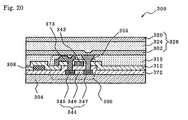
As shown in Fig. 20, JP-A No. 10-189252 discloses an
active-driving type organic EL display device 300 wherein a
drain region 347 of a TFT 344 is electrically connected to
a lower electrode 302 of an organic EL element 326 are
through a contact hole (via hole) 354 which is vertically
formed in an inter-insulator 313.
However, in the active-driving type organic EL
display device 200 disclosed in the aforementioned JP-A No.
8-330600 and 10-254383, the barrier metal composed of the
metal thin film of the lower layer 250 and the titanium
nitride thin film of the upper layer 251 is horizontally
formed to connect a drain region 236 of the TFT 237 to a
lower electrode 222 of the organic EL element electrically.
Therefore, if a color-converting medium (not shown) such as
a thick color filter or color-converting film is provided
adjacent the lower electrode of the organic EL element 226
for example, the following problems arise: (i) A level-difference
between the drain region of the TFT and the
lower electrode is generated to make it difficult to
connect them electrically to each other; (ii) The barrier
metal is easily damaged so that the reliability of the
connection becomes poor or the like. Although the color-converting
medium was made thin, a new problem that the
color-converting efficiency is lower has been encountered.
If the color-converting medium (not shown) provided
adjacent the lower electrode of the active-driving type
organic EL display device 300 disclosed in the
aforementioned JP-A No. 10-189252 is made thick, the
reliability may be lowered for the electric connection
through the vertically-formed contact hole 354.
That is to say, if the thickness of the color-converting
medium is made, for example, 5 µm or more thick,
the thermal expansion of the color-converting medium
becomes large when the medium is heated, thereby the wires
snapping in the contact hole having a thermal expansion
smaller than that of the color-converting medium.
According to the electric connection using the
vertically-formed contact hole 354, it is difficult that an
electro-conductive material is uniformly filled into the
contact hole since this hole is long. It has been
substantially impossible to use a vapor-deposition method
or a sputtering method, which is an ordinary method for
forming an electrically connecting member.
Thus, the present inventors have made eager
investigations on the above-described problems, thereby
finding out that by disposing an electrically connecting
member obliquely between an organic EL element and a TFT,
superior connection reliability can be obtained with the
above-described problems being solved.
That is, an object of the present invention is to
provide an active-driving type organic EL display device
wherein a lower electrode of an organic EL element can
easily be connected electrically to a drain region of a TFT
even if a color-converting medium having a thickness of,
for example, 5 µm or more is provided adjacent the lower
electrode, so that superior connection reliability can be
obtained.
Another object of the present invention is to provide
a producing method making it possible to supply such an
active-driving type organic EL display device efficiently.
Disclosure of the Invention
[1] According to one aspect of the present invention,
there is provided an active-driving type organic EL display
device comprising an organic EL element made so as to have
an organic luminous medium sandwiched between an upper
electrode and a lower electrode, and a TFT for controlling
luminescence of the organic EL element, wherein the
luminescence of the organic EL element is taken out from
the lower electrode, a color-converting medium provided
adjacent the lower electrode, and an inclined electrically
connecting member is provided between the lower electrode
and the TFT.
Namely, the organic EL display device having such a
structure makes it possible to form the electrically
connecting member easily between the organic EL element and
the TFT and to obtain superior connection reliability.
[2] When producing the active-driving type organic EL
display device of the present invention, it is preferred
that the inclination angle of the electrically connecting
member to a horizontal plane is set to a value within the
range of 10° to 80°.
The setting of the electrically connecting member to
have such an inclination angle makes it possible to obtain
better electric connection between the organic EL element
and the TFT and makes the formation of the electrically
connecting member to be formed easier.
[3] When producing the active-driving type organic EL
display device of the present invention, it is preferred
that an inclined plane be made in part of the color-converting
medium, and that the electrically connecting
member be disposed along the inclined plane.
Such a structure makes it possible to use a side of
the color-converting medium as a supporting portion for the
electrically connecting member and to set the inclined
electrically connecting member easily, and further to
improve the durability of the electrically connecting
member.
[4] When producing the active-driving type organic EL
display device of the present invention, it is preferred
that the electrically connecting member be a via hole
formed in an inter-insulator provided between the organic
EL element and the TFT.
If the electrically connecting member is the via hole
described above, it is easy to set the electrically
connecting member so as to be inclined. Moreover, the
electrically connecting member can contact to the organic
EL element and TFT with the wide area.
[5] When producing the active-driving type organic EL
display device of the present invention, it is preferred
that an oblique member for inclining the electrically
connecting member be disposed at a side end of the color-converting
medium.
By making the oblique member an exclusive supporting
holder for the electrically connecting member, -the
electrically connecting member can be formed precisely and
further the durability and the like of the electrically
connecting member can be improved.
[6] When producing the active-driving type organic EL
display device of the present invention, it is preferred
that the electrically connecting member be an electric wire
made of a sintered electro-conductive paste.
If the electrically connecting member is the electric
wire made of the sintered electro-conductive paste as
described above, it is easy to set the electrically
connecting member inclined. By using the electro-conductive
paste for the electric wire, superior adhesion can be
obtained for the lower electrode and the TFT. Furthermore,
using the electro-conductive paste makes it possible to
utilize the side of the color-converting medium
conveniently as the supporting portion for the electrically
connecting member. Therefore, the durability of the
resultant electrically connecting member can also be
improved.
[7] When producing the active-driving type organic EL
display device of the present invention, it is preferred
that the electrically connecting member be a bonding wire.
The electrically connecting member having such a
structure makes it possible to attain electric connection
between the lower electrode and the TFT easily and promptly
even if a level-difference due to providing the color-converting
medium and the like is generated.
[8] When producing the active-driving type organic EL
display device of the present invention, it is preferred
the electrically connecting member be made of indium zinc
oxide (IZO).
Since indium zinc oxide (IZO) is an amorphous
compound (non-crystal structure) and is superior in etching
properties, the electrically connecting member can be
disposed precisely.Indium zinc oxide (IZO) has good affinity with a
metal thin film made of aluminum, gold or the like. Thus,
superior electric connection properties can be obtained.Furthermore, indium zinc oxide (IZO) makes it
possible to form a denser film and is resistant to stress
destruction, as compared with ITO and the like, which are
crystalline compounds. Therefore, IZO is superior in
moisture resistance and durability. Accordingly, superior
electric connection properties can be obtained greater than
a long period even if the electrically connecting member is
formed to have an inclined plane.
[9] When producing the active-driving type organic EL
display device of the present invention, it is preferred
that the lower electrode be made of indium zinc oxide (IZO)
or indium tin oxide (ITO).
Such a structure makes light-transmissivity of the
lower electrode superior, and makes it possible to perform
charge injection into the EL element at a low resistance.
Furthermore, in case that indium zinc oxide (IZO) is used
as the electrically connecting member, better electric
connection properties can be obtained.
[10] When producing the active-driving type organic
EL display device of the present invention, it is preferred
that the lower electrode and the electrically connecting
member be integrally made of a non-crystalline electro-conductive
oxide, for example, indium zinc oxide.
Such a structure makes it easy to form the display
device and makes it possible to reduce the number of
electrically connecting spots.
[11] When producing the active-driving type organic
EL display device of the present invention, it is preferred
that a part of the electrically connecting member be
provided with a metallized portion.
Such a structure makes it possible to make connection
resistance lower at electrically connecting spots between
the electrically connecting member and the organic EL
element or the TFT.
[12] When producing the active-driving type organic
EL display device of the present invention, it is preferred
that the electrically connecting member be set to a value
within the range of 0.01 to 100 µm.
Such a structure makes it possible to make resistance
loss small in the electrically connecting member, and to
obtain a desirable durability or film-forming properties.
[13] According to another aspect of the present
invention, there is provided an active-driving type organic
EL display device comprising an organic EL element made so
as to have an organic luminous medium sandwiched between an
upper electrode and a lower electrode, and a TFT for
controlling luminescence of the organic EL element, wherein
the luminescence of the organic EL element is taken out
from the lower electrode, a color-converting medium is
provided adjacent the lower electrode, and the color-converting
medium is embedded in both or either of an
inter-insulator and a supporting substrate.
Such a structure makes it possible to decrease a
level-difference between the TFT and the lower electrode
set on the color-converting medium, thereby easily
connecting the TFT to the lower electrode and further
obtaining superior connection reliability.
[14] According to still another aspect of the present
invention, there is provided an active-driving type organic
EL display device comprising an organic EL element made so
as to have an organic luminous medium sandwiched between an
upper electrode and a lower electrode, and a TFT for
controlling luminescence of the organic EL element, wherein
the luminescence of the organic EL element is taken out
from the lower electrode, a color-converting medium is
provided adjacent the lower electrode, and a level
adjusting layer for adjusting the level of the TFT is
disposed between the TFT and the supporting substrate.
Such a structure makes it possible to make the level
of the TFT substantially equal to that of the lower
electrode of the organic EL element. Therefore, the
electric connection can be more easily attained and further
superior connection reliability can be gained.
[15] According to still another aspect of the present
invention, there is provided a method of producing an
active-driving type organic EL display device comprising an
organic EL element made so as to have an organic luminous
medium sandwiched between an upper electrode and a lower
electrode, a color-converting medium for converting the
color of EL luminescence taken out from the lower
electrode, and a TFT for controlling luminescence of the
organic EL element, wherein the producing method comprises
the steps of:
forming the TFT, forming the color-converting medium, forming the electrically connecting member so as to
be inclined, and forming the organic EL element.
Such producing method makes it possible to obtain an
organic EL display device capable of performing full color
display and having superior connection reliability.
[16] When carrying out the method of producing the
active-driving type organic EL display device of the
present invention, it is preferred that the method further
comprise the step of making an inclined plane in a side end
of the color-converting medium, and provide the
electrically connecting member along the inclined plane in
the step of forming the inclined electrically connecting
member.
Such a producing method enables the electrically
connecting member to be formed more easily. The resultant
electrically connecting member is formed along the inclined
plane of the color-converting medium. Therefore, even if
the color-converting medium expands by heat, the
electrically connecting member can follow the expanding
color-converting medium easily.
[17] When carrying out the method of producing the
active-driving type organic EL display device of the
present invention, it is preferred that the lower electrode
and the electrically connecting member are integrally made
of indium zinc oxide.
By carrying out the method in this way, the
electrically connecting member and the lower electrode can
easily be formed in a short time. Resistance loss can also
be lowered by reducing the number of the electrically
connecting spots.
[18] When carrying out the method of producing the
active-driving type organic EL display device of the
present invention, it is preferred that the electrically
connecting member be formed by a vacuum vapor deposition
method or a sputtering method.
Consequently, the electrically connecting member can
be formed easily, using the inclined plane of the color-converting
medium and the like. Furthermore, superior heat
resistance and vibration resistance can be obtained because
the resultant electrically connecting member is a uniform
thin film.
[19] When carrying out the method of producing the
active-driving type organic EL display device of the
present invention, it is preferred that the electrically
connecting member be formed by using a sol-gel method.
Consequently the electrically connecting member can
easily be formed without using any special forming machine
and only by applying a raw material solution (sol) and
thereafter by heating and reducing the sol.
[20] When carrying out the method of producing the
active-driving type organic EL display device of the
present invention, it is preferred that the method further
comprise the step of metallizing at least one part of the
electrically connecting member.
Such producing method makes it possible to lower
connection resistance at connection spots, and to obtain
the superior electrically connecting member.
Brief Description of the Drawings
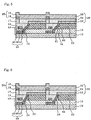
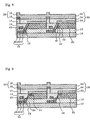
Fig. 1 is a sectional view of an active-driving type
organic EL display device in a first embodiment.
Figs. 2(a) to 2(d) are views showing structure
examples of a lower electrode.
Fig. 3 is a circuit diagram showing an electric
switch connection structure including TFTs.
Fig. 4 is a transparent plan view showing the
electric switch connection structure including the TFTs.
Fig. 5 is a view showing a modified example (a step
form) of the electrically connecting member.
Fig. 6 is a view supplied to explain an oblique
member.
Fig. 7 is a view showing a modified example (a V-shaped
form) of the electrically connecting member.
Fig. 8 is a view showing a modified example (a via
hole) of the electrically connecting member.
Fig. 9 is a view showing a modified example (having a
metallized part) of the electrically connecting member.
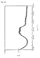
Fig. 10 is a chart showing one example of an X-ray
diffraction of indium zinc oxide (IZO).
Fig. 11 is a sectional view of an active-driving type
organic EL display device in a second embodiment.
Fig. 12 is a view supplied to explain a level
position adjusting layer for TFTs.
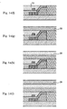
Figs. 13(a) to 13(e) are producing step views showing
the steps in a third embodiment (a first example).
Figs. 14(f) to 14(i) are producing step views showing
the steps in the third embodiment (a second example).
Figs. 15(a) to 15(i) are views showing parts of the
steps for forming a TFT.
Fig. 16 is a view showing a modified example (a
bonding wire) of the electrically connecting member.
Fig. 17 is a view showing a modified example
(integrally formed) of the electrically connecting member.
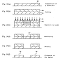
Figs. 18(a) to 18(f) are views showing one example of
etching steps of the electrically connecting member.
Fig. 19 is a sectional view of a conventional active-driving
type organic EL display device (a first example).
Fig. 20 is a sectional view of a conventional active-driving
type organic EL display device (a second example).
Best Mode for Carrying Out the Invention
Hereinafter, embodiments of the present invention
will be specifically described referring to the drawings.
The drawings which are referred to roughly show the size,
the shape and the arrangement relationship of respective
constituent members to such a degree that this invention
can be understood. For example, electric connection between
TFTs and signal electrodes or common electrodes may not be
represented. Therefore, this invention is not limited to
illustrated examples. In the drawings, hatching, which
represents a cross section, may be omitted.
[First embodiment]
As shown in Fig. 1, an organic EL display device of a
first embodiment is an active-driving type organic EL
display device 30 comprising a supporting substrate 10, a
TFT 14 embedded in an inter-insulator (gate insulation
film) 12 formed on the supporting substrate 10, an inter-insulator
(flattening film) 13 and a color-converting
medium 60, each of which is formed on the inter-insulator
12, an organic EL element 26 formed on these inter-insulator
13 and a color-converting medium 60, and an
inclined electrically connecting member 28 for connecting
the TFT 14 to the organic EL element 26 electrically.
Hereinafter, the constituent elements and the like in
the first embodiment will be described referring to Fig. 1
and other figures.
1. Supporting substrate
The supporting substrate (which may be referred to as
the substrate, hereinafter) in the organic EL display
device is a member for supporting the organic EL element,
the TFT and the like, and it is preferred that the
substrate be superior in mechanical strength and
dimensional stability.
Specific examples of such a substrate include glass
plates, metal plates, ceramic plates or plastic plates
(made of polycarbonate resin, acrylic resin, vinyl chloride
resin, polyethylene terephthalate resin, polyimide resin,
polyester resin, epoxy resin, phenol resin, silicone resin,
fluorine resin, and the like).
In order to avoid water invasion into the organic EL
display device, it is preferred that the substrate made of
such a material be subjected to moisture-proof treatment or
hydrophobic treatment by forming an inorganic film or
coating fluorine resin thereon.
Particularly to avoid water invasion into the organic
luminous medium, it is preferred that the percentage of
water content and the gas permeability of the substrate be
restricted. Specifically, the percentage of water content
and the gas permeability of the substrate are preferably
restricted to 0.01% or less by weight and 1 × 10-13
cc·cm/cm2·sec.cmHg or less, respectively.
2. Organic EL element
(1) Organic luminous medium
The organic luminous medium can be defined as a
medium comprising an organic luminous layer capable of
electroluminescence by means of recombination an electron
with a hole. This organic luminous medium can be formed,
for example, by depositing one of the following layers on
the lower electrode:
In general, the structure iv), among these
structures, is favorably used since this structure can give
a higher luminescence brightness and is superior in
durability.
1 ○ Constituent material
Examples of the luminous material of the organic
luminous medium include p-quarterphenyl derivatives, p-quinquephenyl
derivatives, benzothiazole compounds,
benzoimidazole compounds, benzoxazole compounds, metal-chelated
oxynoide compounds, oxadiazole compounds,
styrylbenezene compounds, distyrylpyrazine compounds,
butadiene compounds, naphthalimide compounds, perylene
derivatives, aldazine derivatives, pyraziline derivatives,
cyclopentadiene derivatives, pyrrolopyrrole derivatives,
styrylamine derivatives, coumarin derivatives, aromatic
dimethylidine compounds, metal complexes whose ligand is an
8-quinolinol derivative, and polyphenyl compounds or a
combination selected therefrom.
Among these organic luminous materials, 4,4'-bis(2,2-di-t-butylphenylvinyl)biphenyl
(abbreviated to DTBPBBi),
4,4'-bis(2,2-diphenylvinyl)biphenyl (abbreviated to DPVBi)
and derivatives thereof as aromatic dimethylidine compounds
are more preferred, for example, for blue luminous
materials.
It is also suitable to prepare an organic luminous
material having an distyryl arylene skeleton and the like
such as an aromatic dimethylidine compound, as a host
material, which is doped with a fluorescent dye emitting
intense light in the range from blue to red, such as a
coumarin material, or with a fluorescent dye emitting the
same color as the host material. More specifically, the
above-described DPVBi or the like are used as the host
material, and 1,4-bis[4-(N,N-diphenylaminostyrylbenzene)]
(abbreviated to DPAVB) or the like are used as the dopant,
to make it possible to give blue luminescence.
2 ○ Thickness
Although the thickness of the organic luminous medium
is not limited, it is preferably set to a value within the
range of 5 nm to 5 µm, for example.
The reason is as follows. If the thickness of the
organic luminous medium is smaller than 5 nm, luminescence
brightness and durability may be lowered. On the other
hand, if the thickness of the organic luminous medium is
greater than 5 µm, the applied voltage may become high.
Accordingly, the thickness of the organic luminous
medium is more preferably set to a value within the range
of 10 nm to 3 µm, and still more preferably set to a value
within the range of 20 nm to 1 µm.
(2) Electrodes
Hereinafter, the upper electrode and the lower
electrode will be described. However, depending on the
structure of the organic EL element, the upper electrode
and the lower electrode may be equivalent to an anode layer
and a cathode layer, respectively, or to a cathode layer
and an anode layer, respectively.
1 ○ Lower electrode
The lower electrode may be an anode layer or a
cathode layer, depending on the structure of the organic EL
display device. However, in case that the lower electrode
corresponds to an anode layer, it is preferred to use a
metal, an alloy, an electro-conductive compound, or a
mixture thereof having a large work function (for example,
of 4.0 eV or more). Specifically, it is preferred to use
indium tin oxide (ITO), indium zinc oxide (IZO), copper
iodide (CuI), tin oxide (SnO2), zinc oxide (ZnO), gold,
platinum, and palladium or a combination selected
therefrom.
Using these electrode materials, the lower electrode
having a uniform thickness can be formed by a method
capable of depositing a film in a dry process, such as a
vacuum vapor deposition method, a sputtering method, an
ion-plating method, an electron beam vapor deposition
method, a CVD (Chemical Vapor Deposition) method, an MOCVD
(Metal Oxide Chemical Vapor Deposition) method, or a plasma
enhanced CVD.
Since electroluminescence is required to be taken out
from the lower electrode in the present invention, it is
necessary that the lower electrode be made transparent.
Therefore, it is preferred to use the above-described
electrode material to make the transmission of the
electroluminescence to a value of 70% or more.
The film thickness of the lower electrode is not
limited, and is preferably set to a value within the range
of, for example, 10 to 1000 nm, and more preferably set to
a value within the range of 10 to 200 nm.
This is to make the lower electrode conductive and to
obtain a transmission of electroluminescence of 70% or
more.
It is preferred that as shown in Figs. 2(a) and 2(b),
respectively, the lower electrode 22 have its tip portion
29 branched or circular with a hole. It is also preferred
that as shown in Figs. 2(c) and 2(d), respectively, the
lower electrode 22 have the tip portion 29 with depression
vertically or uneven structure.
Such a structure causes the contact area between the
lower electrode and the electrically connecting member 28
to be large, and causes the adhesion therebetween to be
improved, so that the connection resistance can be
effectively lowered.
In Figs. 2(a) to 2(d), the electrically connecting
members 28 are represented by dotted lines to understand
where the electrically connection members are connected. In
these figures, the connecting members could be replaced
with the electrode and vice versa. That is, in Figs. 2(a)
to 2(d), the tips of each electrically connection members
may be represented by a solid line and the tips of each
lower electrode may be may be represented by the dotted
line.
In order to make the lower the connection resistance
between electrode and the electrically connecting member
lower, it is preferred to provide the lower electrode with
a metallized portion or a bump, although not shown.
2 ○ Upper electrode
On the other hand, the upper electrode may be an
anode layer or a cathode layer, depending on the structure
of the organic EL display device. However, in case that the
lower electrode corresponds to, for example, a cathode
layer, it is preferred to use a metal, an alloy, an
electro-conductive compound, or a mixture or inclusion
thereof having a work function smaller (for example,
smaller than 4.0 eV) than that of the anode layer.
Specifically, it is preferred for the electrode to
use sodium, sodium-potassium alloy, cesium, magnesium,
lithium, magnesium-silver alloy, aluminum, aluminum oxide,
aluminum-lithium alloy, indium, rare earth metals, mixtures
of an organic luminous medium and these metals, and
mixtures of an electron injection layer material and these
metals solely or in combination selected therefrom.
The film thickness of the upper electrode is not
limited, and is preferably set to a value within the range
of, for example, 10 to 1000 nm, and more preferably set to
a value within the range of 10 to 200 nm.
This is to obtain a given surface resistance and good
electric connection reliability.
As shown in Fig. 1, the upper electrode 20 is
preferably composed of a main electrode 16 and an auxiliary
electrode 18 made of a material having a resistivity lower
than that of the main electrode 16.
Such a structure makes it possible to reduce the
surface resistance of the upper electrode 20 significantly.
Thus, the density of current flowing through the organic
luminous medium can be reduced, so that the life of the
organic luminous medium can be significantly prolonged.
(3) Inter-insulator
The inter-insulator of the organic EL display device
of the present invention is disposed near or around the
organic EL element and the TFT. The inter-insulator
principally flattens the unevenness of a fluorescent medium
or a color filter, so as to be used as a flattened
undercoat when forming the lower electrode of the organic
EL element. Furthermore, the inter-insulator is used for
electric insulation for forming a high resolution wiring
material, electric insulation (prevention of a short
circuit) between the lower electrode and the upper
electrode of the organic EL element, electric insulation
and mechanical protection of the TFT, electric insulation
between the TFT and the organic EL element, and the like.
Therefore, the inter-insulator may be referred to as
a flattening film, an electric insulator film, a barrier, a
spacer or the like, if necessary. The Term of "inter-insulator"
in the present invention implies all of them.
1 ○ Constituent material
Examples of the constituent material used in the
inter-insulator generally include organic substances such
as acrylic resin, polycarbonate resin, polyimide resin,
fluorinated polyimide resin, benzoguanamine resin, melamine
resin, cyclic polyolefin, Novolak resin, polyvinyl
cinnamate, cyclic rubber, polyvinyl chloride, polystyrene,
phenol resin, alkyd resin, epoxy resin, polyurethane resin,
polyester resin, maleic acid resin, and polyamide resin.
In case that the inter-insulator is made of an
inorganic substance, preferred examples of the inorganic
substance include silicon oxide (SiO2 or SiOx), aluminum
oxide (Al2O3 or AlOx), titanium oxide (TiO2), yttrium oxide
(Y2O3 or YOx), germanium oxide (GeO2 or GeOx), zinc oxide
(ZnO), magnesium oxide (MgO or MgOx), calcium oxide (CaO),
boric acid (B2O3), strontium oxide (SrO), barium oxide
(BaO), lead oxide (PbO), zirconia (ZrO2), sodium oxide
(Na2O), lithium oxide (Li2O), potassium oxide (K2O), silicon
nitride (Si3N4), silicon nitride oxide (SiOxNY) and calcium
fluoride (CaF2). The values x and Y in the structural
formulae representing the inorganic substances are within
the range of 0.1 to 3.
Particularly in case that heat-resistance is
required, it is preferred to use acrylic resin, polyimide
resin, fluorinated polyimide, cyclic polyolefin, epoxy
resin, or inorganic substances among these constituent
materials.
These inter-insulators are preferably processed into
a desire pattern by introducing light-sensitive groups into
the constituent materials and thereafter by using
photolithography, otherwise by printing.
2 ○ Thickness of the inter-insulator
The thickness of the inter-insulator depends on the
resolution of display, as well as unevenness of a
fluorescent medium or a color filter combined with the
organic EL element. It is preferably within the range of 10
nm to 1 mm.
This is because such a structure makes it possible to
flatten the unevenness of the fluorescent medium or the
color filter sufficiently and to reduce the viewing angle
dependency of high resolution display.
Accordingly, the thickness of the inter-insulator is
more preferably 100 nm to 100 µm, and still more preferably
100 nm to 10 µm.
3 ○ Forming method
The method for forming the inter-insulator is not
limited. The layer is preferably formed, for example, by a
spin coating method, a casting method, a screen-printing
method or the like. It is also preferable to form by a
sputtering method, a vapor-deposition method, a chemical
vapor deposition method (CVD method), ion plating method or
the like.
3. Thin film transistor (TFT)
(1) Structure
As shown in Figs. 1 and 3 to 4, an embodiment of the
active-driving type organic EL display device in the first
embodiment has at least one TFT 14 and an organic EL
element 26 driven by this TFT 14 on a substrate 10.
A color-converting medium 60 and an inter-insulator
13 whose surface is made flat are arranged between the TFT
14 and a lower electrode 22 of the organic EL element 26. A
drain 47 of the TFT 14 is electrically connected to the
lower electrode 22 of the organic EL element 26 through an
electrically connecting member 28 arranged in the boundary
between the inter-insulator 13 and the color-converting
medium 60.
As shown in a circuit diagram of Fig. 3, a plurality
of scanning electrode lines (Yj-Yj+n) 50, (the number of
which is n is 1 to 1000, for example), and signal electrode
lines (Xi-Xi+n) 51 arranged in an XY matrix are
electrically connected to the TFT 14. Furthermore, common
electrode lines (Ci-Ci+n) 52 arranged in parallel to the
signal electrode lines 51 are electrically connected to the
TFT 14.
It is preferred that these electrode lines 50, 51 and
52 be electrically connected to the TFT 14 and constitute
an electric switch for driving the organic EL element 26
together with a condenser 57. In other words, it is
preferred that this electric switch be electrically
connected to the scanning electrode line 50 and the signal
electrode line 51 and the like, and be composed of for
example, at least one first transistor (which may be
referred to as Tr1, hereinafter) 55, a second transistor
(which may be referred to as Tr2, hereinafter) 14 (56), and
a condenser 57.
It is preferred that the first transistor 55 have a
function for selecting a luminous pixel and the second
transistor 56 have a function for driving the organic EL
element.
As shown in Fig. 1, an active layer 44 in the first
transistor (Tr1) 55 and the second transistor (Tr2) 56 are
composed of semiconductor regions 45 and 47 doped into an n
type and of a non-doped semiconductor region 46 not doped,
and can be represented as n+/i/n+.
The source 45 and the drain 47 is assigned to the
respective semiconductor region doped into the n type. They
constitute the transistors 55 and 56 as a whole together
with a gate 43 deposited through a gate oxide film 12 on
the non-doped semiconductor region.
In the active layer 44, the semiconductor regions 45
and 47 doped into the n type may be doped into the p type
so as to make a structure of p+/i/p+. The active layer 44
in the first transistor (Tr1) 55 and the second transistor
(Tr2) 56 is preferably made of an inorganic semiconductor
such as polysilicon or of an organic semiconductor such as
thiophene oligomer or poly(p-phenylenevinylene).
Polysilicon is a particularly preferred material since it
is far more stable against electricity than amorphous Si
(α-Si) when the electric current is supplied.
(2) Driving method
Next, the method for driving the organic EL element
by the TFT will be described.
As shown in a circuit diagram of Fig. 33, it is
preferred that the TFT comprise the first transistor (Tr1)
55 and the second transistor (Tr2) 56, and that further the
TFT constitute the electric switch.
Consequently, switching is executed by inputting a
scanning pulse and a signal pulse through the XY matrix, so
that the organic EL element 26 can be driven.
More specifically, an image can be displayed by
inducing or stopping light emission from the organic EL
element 26 by means of the electric switch.
When the organic EL element 26 is driven in this way
by means of the electric switch, a desired first transistor
55 is selected by a scanning pulse transmitted through the
scanning electrode line (which may be referred to as a gate
line) (Yj-Yj+n) 50 as well as a signal pulse transmitted
through the signal electrode line (Xi-Xi+n) 51, so that a
given electrical charge is supplied to the condenser 57
formed between the common electrode line (Ci-Ci+n) 52 and
the source 45 of the first transistor (Tr1) 55.
In this way, the gate voltage of the second
transistor (Tr2) 56 turns into a constant value and the
second transistor (Tr2) 56 turns into an ON state. Since in
this ON state the gate voltage is held until a next gate
pulse is transmitted, electric current continues to be
supplied to the lower electrode 22 connected to the drain
47 of the second transistor (Tr2) 56.
Accordingly, the organic EL element 26 can be driven
by the supplied current. Thus, the driving voltage for the
organic EL element 26 can be significantly reduced and the
luminous efficiency thereof improves. Moreover, power
consumption can be reduced.
4. Electrically connecting member
(1) Structure 1
As shown in Fig. 1, in the first embodiment, it is
necessary to make the electrically connecting member 28
oblique. Because it is easy to form the electrically
connection element 28. Furthermore, good connection
reliability can be obtained since the electrically
connecting member 28 acts like a spring between the organic
EL element 26 and the TFT 14.
In case that the electrically connecting member 28 is
made oblique, as shown in Fig. 1, it is preferred that the
inclination angle () (the angle how the electrically
connecting member 28 is inclined to the horizontal plane
100) be set to a value within the range of 10° to 80°.
The reason for this is as follows. If this
inclination angle is greater than 80°, it may be difficult
to form the electrically connecting member. On the other
hand, if the inclination angle is smaller than 10°, the
aperture ratio may be significantly lowered.
Therefore, the inclination angle of the electrically
connecting member is more preferably set to a value within
the range of 20° to 70°, and is still more preferably set to
a value within the range of 30° to 60°.
(2) Structure 2
As shown in Fig. 1, it is preferred that a side end
61 of the color-converting medium 60 constitute an inclined
plane 62 and that the electrically connecting member 28 be
disposed along this inclined plane 62.
Such a structure makes it possible to use the side
end 61 of the color-converting medium 60 as a supporting
section for the electrically connecting member 28 and to
easily dispose the inclined electrically connecting member
28 on the color-converting medium 60.
Such a structure makes it possible that the
electrically connecting member 28 follows the expanding
color-converting medium 60 easily even if the color-converting
medium 60 is heated and thermally expands. Thus,
superior connection reliability can be obtained. The
inclined electrically connecting member 28 can easily be
made, for example, only by forming the side end 61 of the
color-converting medium 60 in such a way to be the inclined
plane 62 having an inclination angle of 10° to 80° and by
depositing thereon a metal thin film with a sputtering
method or the like.
(3) Structure 3
A part of the inclined electrically connecting member
preferably contains a horizontal portion or a vertical
portion. Therefore, for example, as shown in Fig. 5, the
electrically connecting member 28 is preferably formed
step-shaped.
Such a structure causes the electrically connecting
member 28 to act like a spring between the organic EL
element 26 and the TFT 14, and makes the electrically
connecting member 28 adhere to the inclined plane well.
Thus, better connection reliability can be obtained.
(4) Structure 4
As shown in Fig. 6, it is preferred that an electric
insulator material be used to form an oblique member 63
attached to the side end 61 of the color-converting medium
60.
Providing the oblique member 63 makes it possible to
give superior connection reliability via the electrically
connecting member 28 even if the color-converting medium 60
is thermally expanded, since the oblique member 63
functions as a buffer member. Providing the oblique member
63 makes it possible to form the inclined electrically
connecting member 28 easily without causing the color-converting
medium 60 to have any inclined plane. This
oblique member may be formed as a flattening film on the
color-converting medium.
It is preferred that the oblique member 63 be made of
the electric insulator material similar to that for the
inter-insulator. Therefore, it is preferred to use, for
example, acrylic resin, polyimide resin, fluorine resin,
polyolefin resin, epoxy resin, silicon oxide (SiO2),
aluminum oxide (Al2O3), titanium oxide (TiO2), silicon
nitride (Si3N4), or the like.
The form of the oblique member 63 is not limited so
long as it partially has an inclined plane. In general, the
oblique member preferably has a triangular form.
(5) Structure 5
As shown in Fig. 7, it is also preferred that by
making two inclined planes, which roughly take a V-shaped
form, in a middle part of the color-converting medium 60,
two electrically connecting members (a first electrically
connecting member 27 and a second electrically connecting
member 28) are provided adjacent the V-shaped inclined
planes.
Such a structure makes it possible to make the
connection resistance lower since the two electrically
connecting members 27 and 28 are electrically connected to
the lower electrode 22, and makes it possible to improve
the connection reliability.
The respective inclination angle () of the two
electrically connecting members 27 and 28 are preferably
set to values within the range of 40° to 80°. Setting this
inclination angle makes it possible to lower decreasing the
aperture ratio of pixels even if the two electrically
connecting members 27 and 28 are disposed.
It is not necessarily required to make the
inclination angles () of the electrically connecting
members 27 equal to that of the electrically connecting
member 28. On one hand, the inclination angle of the first
electrically connecting member 27 may be set to a value
within the range of 10° to 40°. On the other hand, the
inclination angle of the second electrically connecting
member 28 may be set to a value within the range of 40° to
80°.
(6) Structure 6
As shown in Fig. 8, it is preferred that an
electrically connecting member 40 be an inclined via hole
formed through inside the inter-insulator 13 or in a
boundary area between the inter-insulator 13 and the color-converting
medium 60.
If the electrically connecting member 40 is the via
hole as described above, it is easy to make the
electrically connecting member 40 be inclined. Moreover,
good electric connection properties can be obtained since
the contact area with the lower electrode 22 and the
contact area with the TFT 14 can be made large.
It is preferred to set the diameter of the via hole,
which is actually the electrically connecting member 40, to
a value within the range of 0.1 to 100 µm. The reason for
this is as follows. If the diameter of the via hole is
smaller than 0.1 µm, it may be difficult to form the via
hole. The connection reliability may be lowered. On the
other hand, if the diameter of the via hole is greater than
100 µm, it may be difficult to form the via hole. A short
circuit may happen between the adjacent via holes.
It is preferred that the via hole, which is nothing
but the inclined electrically connecting member 40 be
formed by photo etching or mechanical cutting, for example.
(7) Structure 7
As shown in Fig. 9, it is preferred that the
electrically connecting member 28 be made of an electro-conductive
inorganic material (including non-crystalline
electro-conductive oxide) and that a part or the entire
surface of the electrically connecting member be provided
with the metallized portions 31 and 35.
Such a structure makes it possible to make lower the
connection resistance at each of electrically connecting
sites between the electrically connecting member 28 and the
lower electrode of organic EL element 26, as well as the
ones between the electrically connecting member 28 and the
TFT 14.
Two of the metallized portions 31 and 35 may be made
of the same forming material or made of different
materials. Preferred examples of the material of the
metallized portions include aluminum, platinum, gold,
silver, copper, palladium, nickel, chromium, tantalum,
tungsten, molybdenum, titanium, titanium nitride (TiN),
tantalum nitride (TaN), silver-palladium-copper alloy (APC)
and the like or a combination selected therefrom. By using
these metals, the connection resistance of the connecting
ends can surely be made low.
It is particularly preferred that titanium,
molybdenum, chromium or APC is used in the metallized
portion 31, and chromium or tungsten be used in the
metallized portion 35. Such a structure makes it possible
to lower the connection resistance of the connecting ends
at the upper side (31) as well as the lower side (35) and
to improve corrosion-resistance of the both sides.
Furthermore, the method for forming the metallized
portions is not limited. It is preferred to adopt, for
example, a plating method, a vapor deposition method, or a
sputtering method.
When deciding the thickness of the metallized
portions, it is preferred to take into consideration the
connection resistance of the electrically connection spots.
Specifically, it is preferred to set the thickness to a
value within the range of 0.01 to 50 µm.
The reason for this is as follows. If the thickness
of the metallized portions is smaller than 0.01 µm, the
connection resistance of the electrically connection spots
may not be lowered. On the other hand, if the thickness is
greater than 50 µm, it may take much time to form the
metallized portions.
Therefore, the thickness of the metallized portions
is more preferably set to a value within the range of 0.01
to 30 µm, and is still more preferably set to a value
within the range of 0.03 to 10 µm.
(8) Structure 8
The thickness of the electrically connecting member
28 is preferably set to a value within the range of 0.01 to
100 µm.
The reason for this is as follows. If the thickness
of the electrically connecting member is smaller than 0.01
µm, the durability thereof may deteriorate. Further, Its
resistance loss may become significantly large. On the
other hand, if this thickness is greater than 100 µm, it
may take very much time to form the electrically connecting
member. Further, the electrically connecting member may
become brittle.
Therefore, the thickness of the electrically
connecting member is more preferably to a value within the
range of 0.01 to 80 µm, and still more preferably set to a
value within the range of 0.03 to 50 µm.
(9) Constituent material
1 ○ Kind 1
The constituent material of the electrically
connecting member 28 is not limited as long as it is
conductive. Specific examples of such material include
metal materials, alloy materials, electro-conductive
inorganic materials, organic electric conductors, and
carbon compounds.
Preferred examples of the metal materials include
aluminum (Al), platinum (Pt), palladium (Pd), gold (Au),
silver (Ag), copper (Cu), nickel (Ni), solder (Pd/Sn
alloy), tin (Sn), lead (Pd), magnesium (Mg), molybdenum
(Mo), indium (In), chromium (Cr), tantalum (Ta), titanium
(Ti), tungsten (W), and silver-palladium-copper (APC), and
the like or a combination selected therefrom.
In case that nickel (Ni) is used, electrolytic nickel
obtained by electrolysis polymerization is preferred. This
is because this electrolytic nickel is superior in etching
properties and toughness.
2 ○ Kind 2
Preferred examples of the electro-conductive
inorganic material which constitutes the electrically
connecting member 28 include indium tin oxide (ITO), indium
zinc oxide (IZO), tin oxide (SnO2), zinc oxide (ZnO),
antimony oxide (SbO2), ZnS, ZnSe, ZnSSe, MgS, MgSSe, CdS,
CdSe, CdTe, CdSSe and the like or a combination selected
therefrom.
Among these electro-conductive inorganic materials,
indium zinc oxide (IZO) is preferred since IZO can be made
non-crystalline within a wide sintering temperature range,
for example, of 100 to 700°C, as will be described. The
durability of the obtained electro-conductive inorganic
material (thin film) is also superior.
With indium zinc oxide (IZO), the electrically
connecting member 28 can be formed by using a sol-gel
method. Therefore, it is preferred to employ, as the
starting material, a carboxylate such as indium acetate or
zinc acetate, an inorganic indium compound such as zinc
chloride, or an indium alkoxy compound such as indium
ethoxide or zinc ethoxide.
When employing an indium zinc oxide (IZO) for forming
the electrically connecting member 28, the molar ratio
(represented as In/(In + Zn)) is preferably set to a value
within the range of 0.5 to 0.95.
The reason is as follows. When the molar ratio of
indium is smaller than 0.5, the transparency as well as the
electrical conductivity may be lowered. On the other hand,
if the molar ratio of indium is greater than 0.95, IZO may
easily be crystallized.
Accordingly, the molar ratio (In/(In + Zn)) of indium
is more preferably set to a value within the range of 0.75
to 0.90, and still more preferably set to a value within
the range of 0.8 to 0.90.
The molar ratio of indium can be measured by ICP
(Inductively Coupled Plasma) analysis, AES analysis (Auger
Electron Spectroscopy), XPS (X-ray Photoconductor
Spectroscopy) or the like.
3 ○ Kind 3
Among the electro-conductive inorganic materials of
which the electrically connecting member 28 is made, non-crystalline
electro-conductive oxides are preferred as
described above. Because the properties of the non-crystalline
electro-conductive oxide, such as superior
moisture-resistance and heat-resistance, are useful for
giving good electric connection between the organic EL
element and the TFT.
Superior etching property of the non-crystalline
electro-conductive oxide is useful for easily forming the
electrically connecting member having superior precision.
However, a crystalline structure may be partially
contained in the materials of the electrically connecting
member. The content of the crystalline structure, however,
is preferably restricted up to 3% by weight, more
preferably up to 1% by weight, and still more preferably up
to 0.5% by weight.
The non-crystallinity of the constituent materials of
the electrically connecting member can easily be controlled
by adjusting the conditions (including the kind of a
target) of a vacuum vapor deposition method or a sputtering
method, as well as by adjusting or the kind or the amount
of a dopant to be added. The non-crystallinity of such
constituent materials can be checked by measuring the X-ray
diffraction structure thereof.
For example, Fig. 10 shows an example of X-ray
diffraction chart of indium zinc oxide (IZO). From the fact
that no crystal peak can be observed within the range of 5°
to 60° for 2, it can be confirmed that the constituent
material of the electrically connecting member is non-crystalline.
4 ○ Kind 4
It is also preferred that the non-crystalline
electro-conductive oxide of the electrically connecting
member 28 contains a dopant. Adding the dopant makes it
easy to adjust the conductivity of the non-crystalline
electro-conductive oxide.
Examples of such a dopant include Sn, Sb, Ga, Ge and
the like or a combination selected therefrom.
In case of a sputtering method, such a dopant should
previously be mixed with a sputtering target and thereafter
the sputtering target is used to perform sputtering. On the
other hand, in case of a sol-gel method, it is preferred to
add such a dopant as an alkoxy compound such as dimethoxy
tin, trimethoxy antimony, triethoxy gallium and
tetramethoxy germanium, or a chloride such as tin chloride,
antimony chloride, gallium chloride and germanium chloride
because such a compound can be uniformly added in the state
of sol.
The added amount of the dopant is preferably set to a
value within the range of 0.1 to 30% by weight of the total
non-crystalline electro-conductive oxide.
The reason for this is as follows. If this added
amount of the dopant is smaller than 0.1% by weight, the
effect of adding may not be obtained. On the other hand, if
the amount of the dopant is greater than 30% by weight, the
heat-resistance or the moisture-resistance may be lowered.
Accordingly, the added amount of the dopant is more
preferably set to a value within the range of 1 to 25% by
weight of the total non-crystalline electro-conductive
oxide, and still more preferably set to a value within the
range of 10 to 20% by weight thereof.
5 ○ Kind 5
Preferred examples of the organic electric conductor
of which the electrically connecting member 28 is made
include electro-conductive conjugated polymers, oxidant-added
polymers, reductant-added polymers, oxidant-added low
molecular weight substance, and reductant-added low
molecular weight substance.
Examples of the oxidant added to the organic electric
conductor include Lewis acids, such as iron chloride,
antimony chloride and aluminum chloride. Examples of the
reductant added to the organic electric conductor include
alkali metals, alkali earth metals, rare earth metals,
alkali compounds, alkali earth compounds, and rare earth
compounds, and the like. Furthermore, examples of the
electro-conductive conjugated polymer include polyaniline
and derivatives thereof, polythiophene and derivatives
thereof, and Lewis acid added amine compound layers, and
the like.
The carbon compound is preferably amorphous carbon,
graphite, or diamond-like carbon.
6 ○ Resistivity
The resistivity of the material for the electrically
connecting member 28 is preferably set to a value of 1 ×
10-3 Ω·cm or less.
The reason is that if this resistivity is greater
than 1 × 10⁻³ Ω·cm, resistance loss becomes excessively
large so that the switch operation of the TFT may be
obstructed.
Accordingly, the resistivity of the constituent
material in the electrically connecting member is more
preferably set to a value of 5 × 10⁻⁴ Ω·cm or less, and
still more preferably set to a value of 1 × 10⁻⁴ Ω·cm or
less.
7 ○ Surface resistance
The surface resistance of the electrically connecting
member 28 is preferably set to a value within the range of
0.01 to 100 Ω/□.
The reason for this is as follows. If this surface
resistance is smaller than 0.01 Ω/□, the kinds of the
usable materials are excessively limited and further the
property of electric connection to the lower electrode
(transparent electrode) made of ITO, IZO or the like may be
lowered. On the other hand, if the surface resistance is
greater than 100 Ω/□, resistance loss becomes excessively
large so that the switch operation of the TFT may be
obstructed.
Accordingly, the surface resistance of the
electrically connecting member is more preferably set to a
value within the range of 0.1 to 20 Ω/□, and still more
preferably set to a value within the range of 0.1 to 10 Ω/
□.
5. Color-converting medium
The color-converting medium is a color filter or a
fluorescent medium for emitting light having a color
different from that of electroluminescence, which will be
described. The color-converting medium of the present
invention also includes a combination of these.
(1) Color filter
1 ○ Structure
The color filter is provided to decompose or cut
light, thereby adjusting color or improving contrast. The
color filter is constituted by pigment (dye) layer made
only of a pigment (dye), or a layered-product wherein a
pigment (dye) is dissolved or dispersed in a binder resin.
It is preferred that the color filter contain three
pigments of blue, green and red. Combining such a color
filter with an organic EL element emitting white light
makes it possible to give the three primary colors of
light, that is, blue, green and red, thereby attaining full
color display.
Like the fluorescent medium, the color filter is
preferably patterned by printing method or photolithography
method.
2 ○ Thickness
The thickness of the color filter is not limited so
long as it sufficiently receives or absorb the luminescence
of the organic EL element without disturbing color-converting
function. The thickness is preferably set to a
value within the range of 10 nm to 1 mm, more preferably to
a value within the range of 0.5 µm to 1 mm, and still more
preferably to a value within the range of 1 µm to 100 µm.
If the thickness of the color filter is 5 µm or more,
the level of the lower electrode has proved to be elevated,
thereby the reliability of the electric connection being
lowered between the lower electrode and the TFT. Therefore,
it can be said that the inclined electrically connecting
member of the present invention can exhibit the effect more
effectively in case that the thickness of the color filter
is 5 µm or more.
(2) Fluorescent medium
1 ○ Structure
The fluorescent medium in the organic EL display
device has a function of absorbing luminescence of the
organic EL element and of emitting fluorescence having a
wavelength longer than the electroluminescence. The
fluorescent medium is formed in the form of layered pieces
which is horizontally separated from each other and
arranged. The respective fluorescent medium pieces are
preferably arranged corresponding to luminous areas of the
organic EL elements, for example, at the cross portions of
the lower electrodes and the upper electrodes. This is
because the respective fluorescent medium piece is able to
emit the luminescence having a color (wavelength) different
from that of the incident light when the organic luminous
layer at the cross portions of the lower electrodes and the
upper electrodes emits light. Even if the organic element
emits only blue light, it is possible to obtain three
primaries (blue, green and red) by converting such blue
light to red and green with the fluorescent medium. Thus,
full color display is completed.
It is also preferred to arrange, between the
fluorescent medium pieces, a shading layer (black matrix)
for blocking off the luminescence emitted from each organic
EL element and the light incident from the respective
fluorescent medium piece and for improving contrast so as
to reduce the dependency upon the viewing angle. This
shading layer corresponds to the member 13 of Fig. 1, for
example. The shading layer can be obtained by blackening
the member or by making the member non light-transmissible.
The fluorescent medium may be combined with the
above-described color filter in order to prevent the
lowering of contrast due to outdoor daylight.
2 ○ Forming method
In case that the fluorescent medium is mainly made of
a fluorescent pigment (dye), it is preferred that the
pigment film be formed by vacuum vapor deposition or
sputtering method through a mask for obtaining a desired
fluorescent medium pattern.
On the other hand, in case that the fluorescent
medium is made of a fluorescent pigment (dye) and resin, it
is preferred to subject the fluorescent pigment and the
resin to mixing, dispersing or solubilizing process so as
to prepare a liquid product, subsequently to make the
liquid product be a film by a spin coating method, a roll
coating method, a casting method or the like, and further
subsequently to pattern the film into a desired pattern by
a photolithography method, a screen printing method or the
like.
3 ○ Thickness
The thickness of the fluorescent medium is not
limited as far as the fluorescent medium is not to thick to
receive (absorb) the luminescence emitted from the organic
EL element and to perform the fluorescence-generating
function. For example, the thickness is preferably set to a
value within the range of 10 nm to 1 mm, more preferably
set to a value within the range of 0.5 µm to 1 mm, and
still more preferably set to a value within the range of 1
µm to 100 µm.
If the thickness of the fluorescent medium is 5 µm or
more, the reliability of the electric connection between
the lower electrode and the TFT is lowered. This is the
same as the case of the color filter. Therefore, the
inclined electrically connecting member of the present
invention can exhibit its effect more effectively only when
the thickness of the fluorescent medium is 5 µm or more.
[Second embodiment]
As shown in Fig. 11, the organic EL display device in
the second embodiment is an active-driving type organic EL
display device 36 comprising a supporting substrate 10, a
TFT 14 and a color-converting medium 60 formed thereon, an
organic EL element 26 formed on the color-converting medium
60, an electrically connecting member 28 for connecting the
TFT 14 electrically to a lower electrode 22 of the organic
EL element 26, and a sealing member 58 for covering the
surroundings of the organic EL element 26 and the like.
In the second embodiment, there is provided the
organic EL display device wherein a part or the whole of
the color-converting medium 60 is embedded in both or
either of the inter-insulator (including a gate insulation
film or a flattening film) 12, 13 and the supporting
substrate 10.
Referring to Figs. 11 and 12, the second embodiment
will be described hereinafter.
(1) Embedding structure
As shown in Fig. 11, in the organic EL display device
36 of the second embodiment, a part of the color-converting
medium 60 is preferably embedded in both or either of the
inter-insulators 12, 13 and the supporting substrate 10.
Such a structure makes it possible to fix the color-converting
medium 60 firmly without using any special
fixing means, and to lower the level of the lower electrode
22 formed thereon.
Therefore, the handling of the color-converting
medium 60 becomes easy and further a level difference
between the level of the electrically connecting spot
(drain electrode) in the TFT 14 and the one of the
electrically connecting spot in the lower electrode 22 can
be made small.
Thus, the electrically connecting member 28 can be
made short, so that making electric connection becomes easy
and the resistance loss in the electrically connecting
member can be made small.
How much the color-converting medium is embedded
should be decided based on the easiness of electric
connection between the TFT and the lower electrode and the
reliability of the connection. Specifically, the embedded
quantity of the color-converting medium is preferably set
to a value within the range of 0.1 to 20 µm.
The reason for this is as follows. If this embedded
quantity is smaller than 0.1 µm, the electrically
connecting member 28 is hardly made short in case that the
color-converting medium is thick. On the other hand, if the
embedded quantity is greater than 20 µm, it may be
difficult to embed the color-converting medium.
Therefore, this embedded quantity is more preferably
set to a value within the range of 0.2 to 15 µm, and still
more preferably set to a value within the range of 0.3 to
10 µm.
The method of embedding the color-converting medium
in the inter-insulators or the supporting substrate is not
limited. It is preferred that a part of the color-converting
medium be embedded, for example, by cutting or
etching the corresponding spot of the inter-insulators or
the supporting substrate. By forming the color-converting
medium on the supporting substrate before forming the
inter-insulators, it is also possible to easily embed the
color-converting medium in the inter-insulators.
Although Figs. 11 and 12 illustrate an example
wherein the color-converting medium 60 is partially
embedded in the inter-insulators 12 and 13, it is also
preferred to embed the color-converting medium in both of
the supporting substrate 10 and the inter-insulators 12 and
13. Otherwise, it is also preferable to omit the inter-insulators
12, 13 and to embed a part or the whole of the
color-converting medium 60 only in the supporting substrate
10.
(2) Position adjusting layer
As shown in Fig. 12, in the second embodiment, a
level adjusting layer 33 for adjusting the level of the TFT
14 is preferably disposed between the TFT 14 and the
supporting substrate 10.
Such a structure makes it possible to elevate the
level of the connection spot in the TFT 14 formed on the
position adjusting layer 33 only by changing the thickness
of the position adjusting layer 33. Therefore, it is
possible to make small the level-difference between the
level of the electrically connecting spot in the TFT 14 and
the one of the electrically connecting spot (drain
electrode) in the lower electrode 22, to make the
electrically connecting member 28 short, and to make small
the resistance loss in the electrically connecting member
28.
The thickness of the level adjusting layer should be
decided based upon the easiness of the electric connection
between the TFT and the lower electrode and the reliability
of the connection. Specifically, the thickness of the level
adjusting layer is preferably set to a value within the
range of 0.1 to 20 µm.
The reason is as follows. If the thickness of the
position adjusting layer is smaller than 0.1 µm, the length
of the electrically connecting member 28 is hardly made
short in case that the color-converting medium is thick. On
the other hand, if the thickness of the position adjusting
layer is greater than 20 µm, it may be difficult to form
the position adjusting layer.
Therefore, the thickness of the level adjusting layer
is more preferably set to a value within the range of 0.2
to 15 µm, and still more preferably set to a value within
the range of 0.3 to 10 µm.
The constituent material of the level adjusting layer
is not limited. The same electrically insulating material
as that for the inter-insulator is preferably used.
Therefore, it is preferred to use, for example, an acrylic
resin, a polyimide resin, a fluorine resin, a polyolefin
resin, an epoxy resin, silicon oxide (SiO2), sol-gel glass,
aluminum oxide (Al2O3), titanium oxide (TiO2), silicon
nitride (Si3N4), a glass plate or the like.
The method of forming the level adjusting layer is
not limited. The layer is preferably formed, using, a vapor
deposition method, a sputtering method, a printing method,
an adhesion method, or a photo-curing method using a photo-curing
resin as well as by means of etching or sandblasting
of spots other than the position adjusting layer,.
(3) Sealing member
It is preferred that the sealing member in the
organic EL display device is disposed to the periphery of
the organic EL display device in order to prevent water
from invading inside. Otherwise, or further, a known
sealing medium, for example, drying agent, dry gas, or
inert liquid such as fluoride hydrocarbon, can be inserted
into a space between the organic EL display device and the
sealing member fitted as described above.
For such a sealing member, the same kind of material
as that for the supporting substrate, such as a glass plate
or a metal plate, can be used. The form of the sealing
member is not limited. The sealing member is preferably
formed plated-shaped or cap-shaped, for example. In case
that the sealing member is formed plate-shaped, its
thickness is preferably set to a value within the range of
0.01 to 5 mm.
Furthermore, it is also preferred that a groove or
the like be formed in a part of the organic EL display
device and that the sealing member be injected into the
groove and fixed thereto. Otherwise, it is also preferred
that a photo-curing type adhesive agent or the like be used
to fix the sealing member onto a part of the organic EL
display device.
[Third embodiment]
The third embodiment relates to a method for
producing the organic EL display device 30 of the first
embodiment, illustrated in Fig. 1. The third embodiment is
specifically a method of producing the active-driving type
organic EL display device 30 comprising, the TFT 14
embedded in the inter-insulator 12 formed on the supporting
substrate 10, the organic EL element 26 formed on the
inter-insulator 12 and including the organic luminous
medium 24 sandwiched between the upper electrode 20 and the
lower electrode 22, and the electrically connecting member
28 for electrically connecting the TFT 14 to the organic EL
element 26.
In the third embodiment, as shown in Figs. 13(a) to
13(e), Figs. 14(f) to 14(i) and Figs. 15(a) to 15(i), there
is provided a method for forming the organic EL display
device 30 comprising the steps of forming the TFT 14,
forming the inclined electrically connecting member, and
forming the organic EL element 26.
Hereinafter, referring to these figures and others,
the characteristic parts of the third embodiment will be
described.
(1) Step of forming a thin film transistor (TFT)
Referring to Figs. 15(a) to 15(i), the step of
forming a TFT (the steps of producing an active matrix
substrate) will be described.
1 ○ Forming an active layer
As shown in Fig. 15(a), an α-Si layer 70 is first
deposited on the supporting substrate 10 in a manner such
as low pressure chemical vapor deposition, LPCVD).
The thickness of the α-Si layer 70 is preferably set
to a value within the range of 40 to 200 nm. The substrate
10 is preferably a crystalline material such as quartz, and
is more preferably low-expandable glass. In case that a
low-expandable glass substrate is used, a production
process is carried out at a low temperature, preferably up
to 1000°C, more preferably up to 600°C in order to avoid the
melting or strain of the glass substrate throughout the
production process or avoid the dopant's out-diffusion into
active regions.
Next, as shown in Fig. 15(b), an excimer laser such
as a KrF (248 nm) laser is radiated onto the α-Si layer 70
to perform annealing crystallization thereby obtaining
polysilicon (see SID '96, Digest of technical papers, pp.
17-28).
Referring to the annealing conditions for this
excimer laser, the temperature of the substrate is
preferably set to a value within the range of 100 to 300°C.
In addition, the dose of the excimer laser is set to a
value within the range of 100 to 300 mJ/cm2, respectively.
Next, as shown in Fig. 15(c), the polysilicon
crystallized by the annealing is patterned into an island
form by photolithography. CF4 gas is preferably used for
the etching gas since superior resolution can be obtained.
Next, as shown in Fig. 15(d), an insulator gate
material 72 is deposited on the surfaces of the island-patterned
polysilicon 71 and the substrate 10 by chemical
vapor deposition (CVD) or the like, so as to prepare a gate
oxide insulator layer 72.
This gate oxide insulator layer 72 is preferably made
of silicon dioxide so that chemical vapor deposition (CVD)
such as plasma enhanced CVD (PECVD) or low pressure CVD
(LPCVD) can be applied to the layer 72.
The thickness of the gate oxide insulator layer 72 is
preferably set to a value within the range of 100 to 200
nm.
The temperature of the substrate preferably ranges
from 250 to 400°C. In order to obtain an insulator gate
material of a higher quality, it is preferred that
annealing treatment be conducted at 300 to 600°C for about 1
to about 3 hours.
Next, as shown in Fig. 15(e), a film of a gate
electrode 73 is formed by vapor deposition or sputtering.
Preferred examples of the material for the gate electrode
73 include TaN and Al and the like. The thickness thereof
is preferably set to a value within the range of 200 to 500
nm.
Next, as shown in Figs. 15(f) to 15(h), the gate
electrode 73 is patterned and thereafter anodic oxidization
is performed. When an Al gate is used, the anodic
oxidization is preferably performed two times to complete
insulation, as shown in Figs. 15(f) to 15(h). The method of
the anodic oxidization could be the same as those can be
made to the same content as disclosed in Japanese Patent
Application Publication No. 8-15120.
Next, as shown in Fig. 15(i), an n+ doped region or a
p+ doped region is formed by ion doping (ion implantation),
thereby forming an active layer for a source and a drain.
In order to perform the ion doping effectively, it is
preferred to introduce nitrogen gas during the ion doping
and to heat treatment at 200 to 400°C for 1 to 10 hours.
The gate electrode 73 is preferably made of
polysilicon obtained from α-silicon. Namely, after the
polysilicon gate electrode 73 is formed on the gate
insulation layer, the resultant product is subjected to
ion-implantation with an n-type dopant such as arsenic.
Subsequently, the resultant product is patterned into an
island form by photolithography in such a manner that
source regions and drain regions can be formed in the
polysilicon region.
The above-described gate electrode 73 can be supplied
as a scanning electrode and/or a bottom electrode of a
condenser.
2 ○ Forming signal electrode lines and common electrode lines
After an electric insulation layer, for example, an
SiO layer, is formed on the active layer (not shown) by
ECRCVD (electron cyclotron resonance chemical vapor
deposition), signal electrode lines and common electrode
lines (which may be referred to wiring electrodes) are
formed and electrically connected to each other.
Specifically, of the following steps are conducted: forming
signal electrode lines and common electrode lines; forming
upper electrodes of condensers; connecting electrically the
source of the second transistor (Tr2) 56 to the common
electrode line; connecting electrically the drain of the
first transistor (Tr1) 55 to the signal electrode line.
Together with performing these steps, it is preferred
to form metal lines made of Al alloy, Al, Cr, W, Mo or the
like by a photolithography method and further to form
contacts such as the drains and the sources of the first
transistor (Tr1) 55 and the second transistor (Tr2) 56 by a
vapor deposition method, a sputtering method or the like
with openings of the electric insulation layer deposited on
the side of the surfaces of the contacts being inclined by
etching.
3 ○ Forming an inter-insulator
At the next stage, an inter-insulator made of silicon
dioxide (SiO2), silicon nitride (Si3N4), polyimide or the
like is formed on the whole of the active layer and the
electric insulation layer thereon.
The electric insulation film made of silicon dioxide
can be obtained by a PECVD method under the substrate
temperature of 250 to 400°C with supplying TEOS
(tetraethoxysilane), for example.
The inter-insulator can also be obtained by ECRCVD
method under the substrate temperature of 100 to 300°C.
However, it generally takes much time to make flat
these inorganic insulator film. It is therefore preferred
to form an inter-insulator made of an organic material.
(2) Step of forming an electrically connecting member
1 ○ Forming method 1
The electrically connecting member is preferably
formed with a thin film forming method, that is, both or
either of a vacuum vapor deposition method and a sputtering
method.
Because an electrically connecting member can easily
be obtained with having a uniform thickness even if the
electrically connecting member is formed in an inclined
state.
The electrically connecting member composed of the
such a thin film is superior in durability, thereby giving
superior connection reliability even if the member is
heated or vibrated.
Conditions for the vacuum vapor deposition method and
the sputtering method are not limited. In case that the
electrically connecting member is made of IZO with a DC
sputtering method, the preferable conditions are as
follows: 0.1 to 5 Pa for sputtering gas pressure, 0.1 to 10
W/cm2 for electric power, 5 to 100 nm/minute for film-depositing
rate, and 50 to 200°C for the temperature of a
sputtering face.
2 ○ Forming method 2
It is also preferred to form the electrically
connecting member by sintering an electro-conductive paste.
If the electrically connecting member is an
electrical wiring composed of the sintered substance of the
electro-conductive paste, the electrically connecting
member can be formed only by applying the paste to the
inclined portion and thereafter heating the paste. The
electro-conductive paste has good adhesion to the lower
electrode and the TFT, so that good electric connection
properties can be obtained.
Furthermore, a side of the color-converting medium
can be used for supporting the electrically connecting
member so that the inclined electrically connecting member
can easily be disposed. Moreover, the durability of the
electrically connecting member can be improved.
Sintering conditions of the electro-conductive paste
are not limited. For example, it is preferred to print the
electro-conductive paste in predetermined positions and
thereafter to heat the paste at 80 to 300°C under the non-oxygen
gas for 5 minutes to 20 hours thereby forming the
electrically connecting member.
The kind of the electro-conductive paste is not
limited. For example, the paste can be composed by adding,
to a thermosetting resin such as epoxy resin or phenol
resin, powder of a metal such as Al, Pt, Au, Ag, Cu, Ni or
solder, as well as an electro-conductive inorganic material
such as IZO, In2O3 or SnO2 as an electro-conductive material,
together with a plasticizer or the like as a viscosity
adjuster.
3 ○ Forming method 3
As shown in Fig. 16, the electrically connecting
member 23 is preferably formed by wire bonding method.
Even if a level-difference based on the color-converting
medium 60 or the like has occurred between the
TFT 14 and the lower electrode 22 as a transparent
electrode, the TFT can easily be connected to the lower
electrode 22 only by adjusting the length of the bonding
wire. For example, in case that the thickness of the color-converting
medium is t (µm), by the bonding wire 1.2t to 3t
(µm) long, the TFT can easily be connected to the lower
electrode and further superior connection reliability can
be obtained.
A preferred kind of the material for the bonding wire
is Al, Au, Cu or the like. Because precise electric
connection can be obtained between the lower electrode and
the TFT. The resistance loss is also small.
4 ○ Forming method 4
As shown in Fig. 17, it is preferred to form the
electrically connecting member 28 integral with the lower
electrode 22. It will be confirmed in Fig. 17 that no seam
is drawn between the electrically connecting member 28 and
the lower electrode 22.
Consequently, it is possible to reduce the number of
the electrically connection spots and to obtain the
electrically connecting member having better connection
reliability.
In order to form the electrically connecting member
integral with the lower electrode, it is preferred to adopt
a sputtering method. It is also preferred to adopt a sol-gel
method, which will be described later, using a non-crystalline
electro-conductive oxide.
5 ○ Forming method 5
As aforementioned, it is still preferred to form the
electrically connecting member by a sol-gel method.
Specifically, a raw material solution of an indium zinc
oxide is coated and then converted with heat to a gel for
preparing material of the electrically connecting member.
Subsequently, the gel is patterned with a photolithography
method, thereby producing the electrically connecting
member.
Using this sol-gel method, it is easy to form the
electrically connecting member made of a non-crystalline
electro-conductive oxide. Such an electrically connecting
member can be obtained without using any special forming
device. That is, it is obtained only by applying the raw
material solution onto a predetermined position and
thereafter heating (sintering) as well as reducing the
applied solution. Since sintering temperature or reducing
temperature is relatively low, thermal damage is hardly
given to the other constituent members. Therefore, an
organic element EL can be formed before the electrically
connecting member is formed.
The heating (sintering) condition for the gelation is
not limited. For example, heating is preferably executed at
100 to 700°C for 5 minutes to 20 hours, and more preferably
at 250 to 500°C for 5 minutes to 20 hours.
The reason is as follows. If the heating temperature
is slower than 100°C, the gelation may be insufficient. On
the other hand, if the heating temperature is higher than
700°C, a crystal portion is apt to be formed.
Furthermore, the condition for the reduction is not
limited. For example, it is preferred to heat at 100 to
700°C for 5 minutes to 20 hours and to reduce with such a
reducing gas as hydrogen, nitrogen or argon. Heating is
more preferably executed at 250 to 500°C for 5 minutes to 20
hours.
6 ○ Forming method 6
It is preferred that the electrically connecting
member be made of a non-crystalline electro-conductive
oxide and that the oxide is etched with an organic acid to
form a pattern. Specifically, as shown in Figs. 18(a) to
18(f), photolithography method is used to form a resist
film 80 on a non-crystalline electro-conductive oxide 28
(Figs. 18(a) and 18(b)). Subsequently, the resist film 80
is exposed to light 81 through a photo mask 82 (Fig.
18(c)). A part 28' of the non-crystalline electro-conductive
oxide is then revealed by developing (Fig.
18(d)). Succeedingly, the part 28' is etched with an
organic acid so as to be patterned (Fig. 18(e)). Finally,
the resist film 80 is stripped so that the electrically
connecting member 28 is revealed (Fig. 18(f)).
Even if such a metal material as Al or Cr is used for
a part of the TFT or the organic EL element, only the non-crystalline
electro-conductive oxide is etched without
corroding such a metal material. Thus, the electrically
connecting member 28 can be formed precisely. Furthermore,
metal migration and the like can easily be prevented.
Even in case that the electrically connecting member
is made of the non-crystalline electro-conductive oxide, in
order to make etching rate high, it is preferred to use a
phosphoric acid based etchant or a hydrochloric acid based
etchant besides the organic acid.
Preferred examples of the organic acid include oxalic
acid, acetic acid, and citric acid. Among others, oxalic
acid or acetic acid is preferred since etching the non-crystalline
electro-conductive oxide can be executed
precisely.
For an etching solution, it is preferred to use, the
organic acid dissolved in water, an alcohol solvent, or a
polar solvent or the like. Employing such a solvent makes
it possible to etch the non-crystalline electro-conductive
oxide more precisely.
In this case, it is preferred to set the
concentration of the organic acid to a value within the
range of 0.1 to 50% by weight. The reason for this is as
follows. If the concentration of the organic acid is
smaller than 0.1% by weight, the rate of etching the non-crystalline
electro-conductive oxide may be significantly
lowered. On the other hand, if the concentration of the
organic acid is greater than 50% by weight, the metal
material such as Al or Cr may be corroded.
Therefore, the concentration of the organic acid is
more preferably set to a value within the range of 1 to 30%
by weight, and still more preferably set to a value within
the range of 3 to 20% by weight.
Although the temperature of the etching is not
limited, it is preferable to set a temperature within the
range of 20 to 100°C. The reason for this is as follows.
If the etching temperature is lower than 20°C, the rate of
etching the non-crystalline electro-conductive oxide may be
significantly lowered. On the other hand, if the etching
temperature is higher than 100°C, the metal material such as
Al or Cr may be corroded.
Therefore, the etching temperature is more preferably
set to a temperature within the range of 25 to 80°C, and
still more preferably set to a temperature within the range
of 30 to 60°C.
(3) Step of forming an organic EL element
As shown in Figs. 13(a) to 13(e) and Figs. 14(f) to
14(i), an organic EL element can be formed in sequence of
the following steps: (i) the TFT 14 and the inter-insulator
(including the oblique member and/or the flattening film)
63 or 13 are formed; (ii) successively formed are the
color-converting medium 60, the electrically connecting
member 28, the lower electrode (anode) 22, the inter-insulator
(not shown), and the organic luminous medium 24
(the organic luminous layer, the hole injection layer, the
electron injection layer and the like); (iii) the upper
electrode (cathode) 20 is formed.
The color-converting medium 60 is preferably formed
by a vacuum vapor deposition method, a sputtering method, a
photolithography method, an ink-jet method, a screen
printing method, a micelle disruption method, or the like.
The lower electrode 22 or the upper electrode 20 is
preferably formed by such a method capable of forming a
film in a dry state as a vacuum vapor deposition method or
a sputtering method.
Furthermore, the organic luminous medium 24 is
preferably formed by a vacuum vapor deposition method, a
sputtering method, a spin coating method, the Langumuir-Blodgett
method (LB method), an ink-jet method, a micelle
disruption method, or the like.
The above-described method or the order of forming
the organic EL element can be appropriately varied within
the scope of the objects of the present invention.
For example, the oblique member or the flattening
film may be formed after the color-converting medium 60 is
formed. Alternatively, the inter-insulator 13 may be formed
at the same time when the oblique member or the flattening
film is formed.
Since the drain portion in the TFT 14 may be eroded
or contaminated when the color-converting medium 60 is
formed, it is preferred to use the inter-insulator to
protect the drain portion until the electrically connecting
member 28 is formed. When the electrically connecting
member 28 is connected electrically to the drain portion,
it is preferred to etch the inter-insulator so as to form
an opening.
(4) Sealing step
Concerning the sealing step, it is preferred to form
the organic EL element, to connect this organic EL element
electrically to the TFT, and to fix these elements by
covering these elements with a sealing member.
It is also preferred to insert a sealing gas into a
space between the sealing member and the organic EL element
and the like.
Furthermore, if water is contained in the organic
luminous medium, the inter-insulators, the gate insulation
film and the like, this water may induce the dark spots or
the like to be generated in the organic EL element after
sealing. Therefore, the water content in these organic
materials is preferably set to a value of 0.05% or less by
weight.
In case that a DC voltage is applied to the organic
EL element, luminescence can be observed when the anode and
the cathode are set to the polarities of + and -,
respectively. The applied voltage should be 5 to 40 V. It
is therefore preferred to drive the organic EL element
before the sealing step and to judge the quality of the
deposited film of the organic EL element.
Example
Hereinafter, examples of the present invention will
be described along production and evaluation of an organic
EL display device for conversion into red luminescence.
However, organic EL display devices for conversion
into other luminescence colors (blue, green and like) can
be realized, and multi-colorization or full colorization
can be carried out by arranging different color-converting
media two-dimensionally in respective pixels.
[Example 1]
(1) Production of an organic EL display device
1 ○ Formation of TFTs
Polysilicon TFTs as shown in Fig. 1 were formed on a
glass substrate (OA2 glass, made by Nippon Electric Glass
Co., Ltd.) having a length of 112 mm, a width of 143 mm and
a thickness of 1.1 mm along Figs. 15(a) to 15(i).
At this time, aluminum was used to form gate
electrodes, scanning electrodes, and bottom electrodes of
condensers, and further a dopant was added to silicon
regions corresponding to sources and drains of the TFTs, so
as to form n+ type regions.
Next, an inter-insulator (SiO2) was formed on the
resultant active layer by CRCVD method, so as to have a
thickness of 500 nm. Thereafter, as shown in Fig. 4,
aluminum was used to form signal electrode lines, common
electrode lines, and upper electrodes of the condensers.
Furthermore, electric connection between the source
electrode of each second transistor (Tr2) and the common
electrode and electric connection between the drain of each
first transistor (Tr1) and the signal electrode were
performed.
Electric connection between each TFT and each
electrode was appropriately performed by subjecting the
inter-insulator SiO2 to wet etching with hydrofluoric acid
and using the thus-opened via holes.
2 ○ Formation of a color-converting medium
Next, a red color filter material (V259R:
anthraquinone type pigment-containing acrylate type resist,
made by Nippon Steel Chemical Co., Ltd.) was applied onto
the inter-insulator (SiO2) by spin coating. After drying,
spots corresponding to portions adjacent to the TFTs in
pixels were exposed to ultraviolet rays, and then developed
with 2.38% by weight TMAH (tetramethyl ammonium hydroxide).
Thereafter, the resultant product was subjected to post-baking
in an oven at 220°C for 10 minutes, so as to form a
red color filter (film thickness: 1.0 µm).
Next, coumarin 6: 0.53 g, Basic Violet 11: 1.5 g,
rhodamine 6G: 1.5 g, and an acrylate type resist (V259PA,
the concentration of solid: 50%, made by Nippon Steel
Chemical Co., Ltd.): 100 g were uniformly dissolved to
prepare an ink for a red fluorescent medium. This ink was
applied onto the substrate, on which the red color filter
was previously formed, by spin coating. After drying,
portions corresponding to the red color filter were exposed
to ultraviolet rays in the state that a gap of 500 µm was
made between a photo mask and the substrate. The exposed
product was developed with the above-described 2.38% by
weight TMAH. Thereafter, the product was subjected to post-baking
in an oven at 180°C for 10 minutes, so as to form a
red fluorescent medium (film thickness: 8 µm).
In the color-converting medium composed of the thus
formed red color filter and red fluorescent medium, the gap
was made between the photo mask and the substrate when the
exposure. Therefore, the end of the color-converting medium
pieces was developed and tapered by diffraction of the
light. As a result, the angle made between the side of the
color-converting medium pieces and the substrate along the
plane direction was 45°. Thus, it is possible to use the
end of the color-converting medium pieces as an oblique
member.
3 ○ Formation of electrically connecting members
Next, opening portions in the inter-insulator (SiO2)
were made along the end of the color-converting medium
pieces by etching method. Electrically connecting members
were formed through the opening portions (inclination
angle: 45°) to attain connection to drains of the second
transistors (Tr2). In other words, oblique ends of the
color-converting medium pieces were used to deposit the
electrically connecting members made of Al and having a
thickness of 100 nm into the whole opening portions by
vapor deposition method. Next, photolithography method was
used to form a pattern.
4 ○ Formation of anodes (lower electrodes)
An IZO film having a film thickness of 200 nm was
deposited on the whole of the surface by sputtering method.
A positive resist HPR204 (made by Fuji-Hunt Electronics
Technology Co., Ltd.) was applied onto this IZO film by
spin coating. The resultant product was exposed to
ultraviolet rays through a photo mask for giving dotted
pattern as pixels, developed with TMAH as a developing
solution, and subjected to post-baking treatment.
Next, an aqueous oxalic acid solution (concentration:
5% by weight) was used as an etchant to etch the IZO film.
An stripping solution 104 (made by Tokyo Ohka Kogyo Co.,
Ltd.) was used to remove the positive resist, thereby
forming a dotted IZO pattern as anodes (lower electrodes),
and attaining electric connection between the anodes and
the electrically connecting members (Al).
5 ○ Formation of an inter-insulator
Next, the above-described acrylate type resist was
applied onto the IZO pattern as pixels by spin coating, and
subsequently the resultant product was exposed to
ultraviolet rays through a photo mask for covering the edge
of the IZO pattern and TFTs. Thereafter, TMAH was used as a
developing solution to develop the product, and further the
developed product was subjected to baking treatment at 180°C
so as to be made to a TFT substrate having an inter-insulator.
6 ○ Dehydrating step
The resultant TFT substrate was cleaned with
isopropyl alcohol and ultraviolet rays, and then moved to a
dehydrating unit for performing a dehydrating step. That
is, the TFT substrate was put in a dry box having an inert
gas (nitrogen) circulating section, a dew point controlling
section, and a heating device section (hot plate).
The hot plate was used to heat the substrate in the
dry box up to 80°C. While dry nitrogen was introduced
thereto in this state, the dew point was lowered to -50°C.
The TFT substrate was allowed to stand still for about 2
hour, to remove water in the color-converting medium and
the inter-insulator and water adhering to the surface of
the glass substrate and the like.
7 ○ Formation of an organic luminous medium
The heating by the hot plate was stopped so that the
temperature of the glass substrate was lowered to room
temperature. Thereafter, the TFT substrate was fixed onto a
substrate holder inside a vacuum vapor deposition machine
(made by ULVAC Co., Ltd.) without exposing the substrate to
the air and with keeping the dew point.
The following materials were filled into a heating
boat made of molybdenum inside the vacuum vapor deposition
machine.
As an upper electrode (cathode) material, Al-Li alloy
(Li concentration: 10% by atom) was fitted onto a filament
made of tungsten.
Next, the evacuated pressure in the vacuum vapor
deposition machine was reduced to 665 × 10
-7 Pa (5 × 10
-7
Torr), and an organic luminous medium and the like were
formed by deposition based on evacuating one time, without
breaking the vacuum state from the formation of a hole
injection layer to the formation of cathodes, in such a
manner that the following vapor deposition rate and
thickness would be obtained. The host material (DPVBi) and
the dopant material (DPAVB) of the organic luminous
materials were simultaneously evaporated.
8 ○ Sealing step
Next, a sealing glass substrate (soda-lime glass,
made by Geomatic Co., Ltd.) was deposited on the side of
the cathodes inside a sealing unit into which dry nitrogen
was introduced, and then the surrounding thereof was sealed
with a photocuring adhesive agent TB3102 (made by Three
Bond Co., Ltd.), to produce an organic EL display device as
shown in Fig. 1.
(2) Evaluation of the organic EL display device
1 ○ Measurement of luminescence performance
A DC voltage of 7 V was applied between the lower
electrodes (IZO pattern, anodes) and the upper electrodes
(cathodes), through the scanning electrodes, the signal
electrodes, and the common electrodes, in the resultant
organic EL display device to cause respective pixels (about
230,000 pixels), which were portions where the respective
electrodes crossed each other, to emit light. A Chroma
meter CS100 (made by Minoluta Co., Ltd.) was used to
measure the luminescence brightness so that a value of 100
cd/m2 was obtained.
The CIE chromaticity thereof was measured. As a
result, it was confirmed that red luminescence whose CIEx
was 0.65 and whose CIEy was 0.35 in the CIE chromaticity
coordinates was obtained.
2 ○ Durability test
Next, the resultant organic EL display device was
continuously driven at room temperature for two weeks. As a
result, the dispersion of the luminescence brightness in
the pixels was within ±10%. Thus, it was confirmed that
stable display was kept at a low voltage.
[Example 2]
(1) Production of an organic EL display device
In Example 2, oblique members were set separately
from a color-converting medium and further the inclination
angle of electrically connecting members was set to 45°. In
this way, an organic EL display device was produced.
That is, TFTs and a red color filter as a color-converting
medium were formed in the same way as in Example
1. Next, coumarin 6: 0.53 g, Basic Violet 11: 1.5 g,
rhodamine 6G: 1.5 g, and an acrylate type resist (V259PA,
the concentration of solid: 50%, made by Nippon Steel
Chemical Co., Ltd.): 100 g were uniformly dissolved to
prepare an ink for a red fluorescent medium. This ink was
applied onto the substrate, on which the red color filter
was formed, by spin coating. Furthermore, portions
corresponding to the red color filter were exposed to
ultraviolet rays in the state that no gap was made between
a photo mask and the substrate. The exposed product was
then developed with the above-described 2.38% by weight
TMAH. Furthermore, the product was subjected to baking at
180°C, so as to form a red fluorescent medium (film
thickness: 8 µm). At this time, in the color-converting
medium, no gap was made between the photo mask and the
substrate in the process of the exposure. Therefore,
diffraction of the light was not caused so that the end of
the color-converting medium pieces was made perpendicular.
As a result, the angle made between the side of the color-converting
medium pieces and the substrate was about 90°.
Next, an acrylate type resist (V259PA) was applied
onto the resultant product by spin coating, and the product
was exposed to ultraviolet rays to form a pattern in which
opening portions were made only in drain regions of the
second transistors (Tr2). The product was then developed
with 2.38% by weight TMAH and baked at 180°C to form oblique
members (which may be referred to flattening films, film
thickness: 2 µm). That is, oblique parts wherein the angle
made between the side of the color-converting medium pieces
and the substrate along the plane direction was 45° were
made.
Next, electrically connecting members (the
inclination angle of the electrically connecting members
was 45°), lower electrodes, organic EL element and the like
were formed in the same way as in Example 1. Thus, an
organic EL display device as shown in Fig. 6 was produced.
(2) Evaluation of the organic EL display device
The resultant organic EL display device was evaluated
in the same way as in Example 1. In other words, about
luminescence performance, the luminescence brightness was
98 cd/m2 under the application of a DC voltage of 7 V, and
the CIE chromaticity was as follows: CIEx = 0.65, and CIEy
= 0.35. Thus, red luminescence was obtained.
An durability test was performed in the same way as
in Example 1. As a result, the luminescence brightness of
the respective pixels was uniform (within ±10%). It was
confirmed that stable display was kept at a low voltage.
[Example 3]
(1) Formation of an organic EL display device
In Example 3, oblique members which also functioned
as a black matrix were set separately from a color-converting
medium and further the inclination angle of
electrically connecting members was set to 80°. In this
way, an organic EL display device was produced.
That is, in the same way as in Example 1, TFTs were
formed and subsequently an acrylate type resist (V259BK,
made by Nippon Steel Chemical Co., Ltd.) containing a black
pigment was applied onto the TFT substrate by spin coating.
Next, the resultant product was exposed to ultraviolet rays
through a photo mask so as to form a pattern which opening
portions were made in drain regions of the second
transistors (Tr2) and the corresponding portions of the
color-converting medium. Furthermore, the resultant product
was developed with 2.38% by weight TMAH, and then baked at
220°C. As a result, the resist was insufficiently photo-cured
because the resist was black. Thus, the pattern
flowed so that oblique members (peak film thickness: 10 µm)
which also functioned as a black matrix and had tapered
edges were formed. The angle made between the side of the
oblique members and the substrate was 80°.
Next, a color-converting medium was made under the
same conditions as in Example 1, and further IZO electrodes
(anodes) which functioned as electrically connecting
members and lower electrodes were formed. At this time, the
inclination angle of the electrically connecting members
(angle thereof to the substrate) was 80°.
Next, in the same way as in Example 1, lower
electrodes, organic EL elements, and the like were formed.
In this way, an organic EL display device as shown in Fig.
6 or 17 was produced.
(2) Evaluation of the organic EL display device
The resultant organic EL display device was evaluated
in the same way as in Example 1. In other words, about
luminescence performance, the luminescence brightness was
95 cd/m2 under the application of a DC voltage of 7 V, and
the CIE chromaticity was as follows: CIEx = 0.65, and CIEy
= 0.35. Thus, red luminescence was obtained.
An durability test was performed in the same way as
in Example 1. As a result, the luminescence brightness of
the respective pixels was uniform (within ±10%). It was
confirmed that stable display was kept at a low voltage.
Furthermore, it was confirmed that the presence of
the black matrix caused colors not to spread between pixels
and caused the contrast of display to be improved.
[Example 4]
(1) Formation of an organic EL display device
In Example 4, the inclination angle of electrically
connecting members was set to 10°. In this way, an organic
EL display device was produced. That is, an organic EL
display device as shown in Fig. 1 was produced under the
same conditions as in Example 1 except that only a red
color filter (film thickness: 1.0 µm) was used as a color-converting
medium, and a white luminescence organic EL
element obtained by co-evaporating rubrene (vapor
deposition rate: 0.03 nm/sec.) was used as the dopant of
the organic luminous material. In the resultant organic EL
display device, the inclination angle of the electrically
connecting members (angle thereof to the substrate along
the plane direction) was 10°.
(2) Evaluation of the organic EL display device
The resultant organic EL display device was evaluated
in the same way as in Example 1. About luminescence
performance, the luminescence brightness was 60 cd/m2 under
the application of a DC voltage of 7 V, and the CIE
chromaticity was as follows: CIEX = 0.65, and CIEy = 0.35.
Thus, red luminescence was obtained.
An durability test was performed in the same way as
in Example 1. As a result, the luminescence brightness of
the respective pixels was uniform (within ±10%). It was
confirmed that stable display was kept at a low voltage.
[Example 5]
(1) Production of an organic EL display device
The structure of an embedded color-converting medium
in an organic EL display device was investigated. That is,
in Example 1, TFTs were made, and subsequently a photo
resist film which opening portions was made in portions
where a color-converting medium was to be formed was
formed. Next, the resultant product was subjected to
sandblasting treatment. The photo resist was stripped to
make grooves having a depth of 10 µm in the inter-insulator
(gate insulation layer and the like) and the supporting
substrate. In the same way as in Example 2, a red color
filter and a red fluorescent medium were embedded and
formed in the groove.
Next, an acrylate type resist was applied onto the
substrate, on which the color-converting medium was formed,
by spin coating. Furthermore, the resultant product was
exposed to ultraviolet rays so as to form a pattern which
opening portions were made only in drain regions of the
second transistors (Tr2). Thereafter, the resultant product
was developed with 2.38% by weight TMAH, and then baked at
180°C, to form a flattening film (film thickness: 0.5 µm).
Next, electrically connecting members were formed in
the same way as in Example 1, so that a level-difference
between the drain regions of the Tr2 and the lower
electrodes became significantly small (smaller than 1.0
µm). In the resultant organic EL display device, the
inclination angle of the electrically connecting members
(angle thereof to the substrate along the plane direction)
was 45°.
Next, in the same way as in Example 1, lower
electrodes, organic EL elements, and the like were formed.
In this way, an organic EL display device as shown in Fig.
11 was produced.
(2) Evaluation of the organic EL display device
The resultant organic EL display device was evaluated
in the same way as in Example 1. In other words, about
luminescence performance, the luminescence brightness was
95 cd/m2 under the application of a DC voltage of 7 V, and
the CIE chromaticity was as follows: CIEx = 0.65, and CIEy
= 0.35. Thus, red luminescence was obtained.
An durability test was performed in the same way as
in Example 1. As a result, the luminescence brightness of
the respective pixels was uniform (within ±10%). It was
confirmed that stable display was kept at a low voltage.
[Example 6]
(1) Production of an organic EL display device
The effect of a position adjusting layer in an
organic EL display device was investigated. That is, an
aqueous alkoxy silane solution was printed (sol-gel
coating) in spots where TFTs were to be formed in the glass
substrate of Example 1, and subsequently the resultant
product was subjected to heating treatment at 400°C to make
the gel into glass. In this way, a position adjusting layer
was formed. The thickness of this position adjusting layer
was 10 µm.
Next, TFTs and a color-converting medium were formed
in the same way as in Example 2. Furthermore, an acrylate
type resist was applied onto the substrate, on which the
TFTs and the color-converting medium were formed, by spin
coating. Furthermore, the resultant product was exposed to
ultraviolet rays so as to form a pattern which opening
portions were made only in drain regions of the second
transistors (Tr2). Thereafter, the resultant product was
developed with 2.38% by weight TMAH, and then baked at
180°C, to form a flattening film (film thickness: 0.5 µm).
Next, electrically connecting members were formed in
the same way as in Example 1, so that a level-difference
between the drain regions of the Tr2 and the lower
electrodes became significantly small (smaller than 1.0
µm). In the resultant organic EL display device, the
inclination angle of the electrically connecting members
(angle thereof to the substrate along the plane direction)
was 45°.
Next, in the same way as in Example 1, lower
electrodes and organic EL elements and the like were
formed. In this way, an organic EL display device as shown
in Fig. 12 was produced.
(2) Evaluation of the organic EL display device
The resultant organic EL display device was evaluated
in the same way as in Example 1. In other words, about
luminescence performance, the luminescence brightness was
100 cd/m2 under the application of a DC voltage of 7 V, and
the CIE chromaticity was as follows: CIEx = 0.65, and CIEy
= 0.35. Thus, red luminescence was obtained.
An durability test was performed in the same way as
in Example 1. As a result, the luminescence brightness of
the respective pixels was uniform (within ±10%). It was
confirmed that stable display was kept at a low voltage.
[Comparative Example 1]
(1) Production of an organic EL display device
An organic EL display device was produced in the same
way as in Example 1 except that the electrically connecting
members in Example 1 were set in the vertical direction
(the inclination angle of the electrically connecting
members: 90°) as shown in Fig. 20.
(2) Evaluation of the organic EL display device
The resultant organic EL display device was evaluated
in the same way as in Example 1. In other words, about
luminescence performance, the luminescence brightness was
50 cd/m2 under the application of a DC voltage of 7 V, and
the CIE chromaticity was as follows: CIEx = 0.65, and CIEy
= 0.35. Thus, red luminescence was obtained.
Therefore, in the organic EL display device of
Comparative Example 1, its luminescence brightness was
lower than Example 1, and luminescence flickered in some
pixels and was unstable.
Furthermore, an durability test was performed in the
same way as in Example 1. As a result, luminescence was not
caused from some pixels. Thus, it was found that stable
display was not kept (±30% or more). The reason for this
was probably as follows. Since the inclination angle of the
electrically connecting members (angle thereof to the
substrate) was clearly about 90° (perpendicular), connection
between the drain regions of the Tr2 and the electrically
connecting members and connection between the lower
electrodes and the electrically connecting members were
made unstable.
| | Inclination Angle | Color Filter | Fluorescent Medium | Luminescence Brightness | Durability Test |
| Example 1 | 45° No oblique member | Red | Red | 100 cd/cm2 | ±10% |
| Example 2 | 45° Oblique members were set. | Red | Red | 98 cd/cm2 | ±10% |
| Example 3 | 80° Oblique members were set. | Red | Red | 95 cd/cm2 | ±10% |
| Example 4 | 10° No oblique member | Red | None | | 60 cd/cm2 | ±10% |
| Comparative Example 1 | 90° No oblique member | Red | Red | | 50 cd/cm2 | Greater than ±30% |
According to the active-driving type organic EL
display device of the present invention, a lower electrode
of an organic EL element and a drain region of a TFT can
easily be connected electrically to each other with high
connection reliability by forming an inclined electrically
connecting member even if a color-converting medium is set
onto the side of the lower electrode to cause color
display.
According to the method of producing an active-driving
type organic EL display device of the present
invention, such an active-driving type organic EL display
device can be effectively produced.