EP1178690A2 - Liquid crystal projector and adjusting method thereof - Google Patents
Liquid crystal projector and adjusting method thereof Download PDFInfo
- Publication number
- EP1178690A2 EP1178690A2 EP01306387A EP01306387A EP1178690A2 EP 1178690 A2 EP1178690 A2 EP 1178690A2 EP 01306387 A EP01306387 A EP 01306387A EP 01306387 A EP01306387 A EP 01306387A EP 1178690 A2 EP1178690 A2 EP 1178690A2
- Authority
- EP
- European Patent Office
- Prior art keywords
- liquid crystal
- color
- crystal panels
- adjusting
- signal
- Prior art date
- Legal status (The legal status is an assumption and is not a legal conclusion. Google has not performed a legal analysis and makes no representation as to the accuracy of the status listed.)
- Granted
Links
Images




Classifications
-
- H—ELECTRICITY
- H04—ELECTRIC COMMUNICATION TECHNIQUE
- H04N—PICTORIAL COMMUNICATION, e.g. TELEVISION
- H04N9/00—Details of colour television systems
- H04N9/12—Picture reproducers
- H04N9/31—Projection devices for colour picture display, e.g. using electronic spatial light modulators [ESLM]
- H04N9/3102—Projection devices for colour picture display, e.g. using electronic spatial light modulators [ESLM] using two-dimensional electronic spatial light modulators
- H04N9/312—Driving therefor
-
- H—ELECTRICITY
- H04—ELECTRIC COMMUNICATION TECHNIQUE
- H04N—PICTORIAL COMMUNICATION, e.g. TELEVISION
- H04N9/00—Details of colour television systems
- H04N9/12—Picture reproducers
- H04N9/31—Projection devices for colour picture display, e.g. using electronic spatial light modulators [ESLM]
- H04N9/3102—Projection devices for colour picture display, e.g. using electronic spatial light modulators [ESLM] using two-dimensional electronic spatial light modulators
- H04N9/3105—Projection devices for colour picture display, e.g. using electronic spatial light modulators [ESLM] using two-dimensional electronic spatial light modulators for displaying all colours simultaneously, e.g. by using two or more electronic spatial light modulators
-
- H—ELECTRICITY
- H04—ELECTRIC COMMUNICATION TECHNIQUE
- H04N—PICTORIAL COMMUNICATION, e.g. TELEVISION
- H04N5/00—Details of television systems
- H04N5/74—Projection arrangements for image reproduction, e.g. using eidophor
- H04N5/7416—Projection arrangements for image reproduction, e.g. using eidophor involving the use of a spatial light modulator, e.g. a light valve, controlled by a video signal
- H04N5/7441—Projection arrangements for image reproduction, e.g. using eidophor involving the use of a spatial light modulator, e.g. a light valve, controlled by a video signal the modulator being an array of liquid crystal cells
- H04N2005/745—Control circuits therefor
Definitions
- the present invention relates to a liquid crystal projector apparatus, such as that capable of modulating light from a light source by means of a plurality of liquid crystal panels and projecting synthetic light transmitted or reflected by the liquid crystal panels as a color image, and particularly to a liquid crystal projector and an adjusting method thereof that may prevent luminance variation from occurring in each frame on a display screen of such a liquid crystal display.
- Television receivers and the like have been developed which form a liquid crystal projector with a light source such as a lamp and a plurality of liquid crystal panels or spatial light modulators to project a color image on a screen or the like.
- a light source such as a lamp
- a plurality of liquid crystal panels or spatial light modulators to project a color image on a screen or the like.
- Such a liquid crystal projector generally separates white light emitted from the lamp into three primary colors by means of a dichroic mirror, modulates light of each of the three primary colors by means of a liquid crystal panel, and thereafter combines the three colors of light with each other by means of a dichroic prism or the like. Then the liquid crystal projector projects the combined light onto a screen or the like via a projection optical lens to thereby form a large screen.
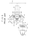
- Fig. 5 is a plan view of a configuration of a three-panel-type liquid crystal projector apparatus formed with one liquid crystal panel for each of the R, G, and B colors (hereinafter referred to simply as a liquid crystal projector).
- the liquid crystal projector apparatus shown in Fig. 5 condenses light emitted from a lamp 21 via an IR/UV cutoff filter in a light source optical system 30, and thereafter performs color separation.
- the light source optical system 30 comprises two microlens arrays 31a and 31b each having a set of microlenses, a polarization beam splitter 32 for aligning a plane of polarization of light, and a condenser lens 33.
- a white luminous flux that has passed through the light source optical system 30 first enters a dichroic mirror 34 for transmitting the red light R. Then, the dichroic mirror 34 transmits the red light R and reflects the green light G and the blue light B. The red light R transmitted by the dichroic mirror 34 is changed in traveling direction by 90° , for example, by a mirror 35, and then guided to a liquid crystal panel 37R via a field lens 36R.
- the green light G and the blue light B reflected by the dichroic mirror 34 are separated by a dichroic mirror 38 for transmitting blue light.
- the green light G is reflected and thereby changed in traveling direction by 90° , for example, and then guided to a liquid crystal panel 37G via a field lens 36G.
- the blue light B passes through the dichroic mirror 38, thus traveling in a straight line, and then guided to a liquid crystal panel 37B via a relay lens 39, a mirror 40, a relay lens 41, a mirror 42, and a field lens 36B.
- the pieces of light of the RGB colors After being subjected to spatial light modulation by the liquid crystal panels 37R, 37G, and 37B, the pieces of light of the RGB colors enter crossed dichroic prisms 43 as a light combining means to be spatially combined with each other. Specifically, the red light R is reflected by a reflection plane 43a and the blue light B is reflected by a reflection plane 43b in a direction of a projection lens 44. The green light G passes through the reflection planes 43a and 43b, whereby the pieces of light of the three colors are combined with each other on a single optical axis.
- the projection lens 44 projects a magnified color image onto a screen 45 hung on a wall, for example, or a flat screen formed as a rear projector.
- the R, G, and B liquid crystal panels 37 employed in the liquid crystal projector as described above generally have a transparent opposite electrode Pf and pixel electrode Pu with liquid crystal intermediate between the opposite electrode Pf and the pixel electrode Pu, as shown in Fig. 6.
- a thin-film transistor TFT serving as a switching device is formed by semiconductor techniques in part of the pixel electrode Pu in a divided pixel unit.
- a gate of each thin-film transistor TFT is connected to a gate bus line Lx formed in a stripe manner in a line direction.
- a source of the thin-film transistor TFT is connected to a source bus line Ly arranged in a direction orthogonal to the gate bus line Lx.
- a drain of each thin-film transistor TFT is connected to a transparent pixel electrode Pu divided for each pixel.
- a liquid crystal capacitance Cis is formed between an opposite electrode Pf and the pixel electrode Pu with liquid crystal intermediate between the opposite electrode Pf and the pixel electrode Pu.
- the source bus lines Ly are sequentially selected in a horizontal direction by an X drive circuit to supply a display signal for one line
- the gate bus lines Lx are sequentially selected in a vertical direction, whereby a signal voltage for each pixel at an intersection of a source bus line Ly and a gate bus line Lx is supplied via a thin-film transistor to charge the liquid crystal capacitance Cis. Display information is thus written to modulate light passing through each liquid crystal pixel and thereby generate an image.
- an auxiliary capacitance Cs as indicated by a dotted line is often formed for the purpose of compensating for leakage current between the source and the drain electrodes.
- black stripes are provided to the opposite electrodes Pf to minimize leak of light passing through portions other than the pixel electrode portions.
- the liquid crystal panel (hereinafter referred to as the LCD panel) comprises an X shift register for sequentially selecting the source bus lines in a line direction to supply a video signal to be written; and a Y shift register for selecting the gate bus lines Lx to take in the supplied signal sequentially in a horizontal direction.
- active matrix driving is performed so that the video signal is written to each pixel in dot sequence or line sequence and the written signal is retained by a capacitance C (Cis + Cs) for a period of one field.
- each LCD panel by direct-current voltage tends to cause electrochemical reaction in liquid crystal material and alignment layer material and at their interface, which results in faulty display. Therefore, in order to prevent application of the DC voltage to each pixel electrode of the LCD panel, an image signal with a field cycle whose polarity is reversed between positive and negative with a Vcom voltage as its center DC level is supplied, as shown in Fig. 7.
- the TFT type LCD panel employs a reversal driving method, in which the LCD panel is driven on the basis of an FRP signal for reversing signal polarity, and a display signal reversed in polarity at least in each field period is supplied to each pixel.
- the conventional reversal driving method adjusts the Vcom voltage shown in Fig. 7 for each LCD so as to minimize the luminance variation of a display image formed by combining images after light modulation by the LCDs with each other by means of a combining prism or the like.
- the detection limit of flicker is very high, and therefore flicker is strongly sensed by the human eye.
- the PAL system in particular, has a low field frequency as compared with the NTSC system, and therefore makes flicker more noticeable.
- an adjusting method for a liquid crystal projector comprising the steps of: driving each of the plurality of liquid crystal panels by an adjusting pattern signal whose polarity is reversed in each frame, and adjusting a direct-current level of the adjusting pattern signal to temporally average light projected by each of the liquid crystal panels; and thereafter adjusting a direct-current level of a driving signal of a part of the liquid crystal panels to temporally average luminance variation of a synthetic projection image modulated and spatially synthesized by the liquid crystal panels.
- the liquid crystal panels can be arranged so as to transmit R color, G color, and B color, and the part of the liquid crystal panels is for the B color.
- the adjusting pattern signal can be a line-reversal alternating-current signal that is reversed in polarity in each horizontal line of the display screen or a dot-reversal alternating-current signal that is reversed in polarity in each pixel in a horizontal direction.
- the driving signal of the G color liquid crystal panel can be formed such that the driving signal of the G color liquid crystal panel is opposite in polarity from driving signals applied to the B color and R color liquid crystal panels.
- a liquid crystal projector with a plurality of liquid crystal panels for forming a display frame by spatially combining pieces of light modulated by the liquid crystal panels with each other, the liquid crystal projector, including: a driving circuit for at least supplying each of the liquid crystal panels with a display signal whose polarity is alternately reversed in each line; and an adjusting means for adjusting a common voltage level of the display signal supplied to each of the liquid crystal panels by the driving circuit; wherein the common voltage levels of the plurality of liquid crystal panels except a part of the liquid crystal panels are adjusted so that luminance variation of light modulated in single-frame units by the liquid crystal panels is minimized; and only the common voltage level applied to the part of the liquid crystal panels is adjusted to a level such that luminance variation in a frame cycle of projection light synthesized by the plurality of liquid crystal panels is minimized.
- the plurality of liquid crystal panels may be for R color, G color, and B color, and the part of the liquid crystal panels is for the B color or the R color, which is low in visibility.
- Each of the LCD panels can be reversed in each frame, and driven by line reversal or dot reversal.
- Polarity of the display signal applied to the G color liquid crystal is opposite in phase to that of the signals applied to the R color and B color liquid crystals.
- the display apparatus using at least two or more LCD panels, supplying image signals by the reversal driving method, and forming a synthetic image adjusts luminance variation of each of the LCD panels during reversal driving to be minimized, and further adjusts luminance variation of light modulated by the LCD panels at a spatially different place. Therefore, the detection limit of flicker on a display screen can be made extremely low. It is thus possible to greatly contribute to reducing flicker especially on a large bright screen.
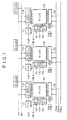
- Fig. 1 shows a principal part of an LCD panel driving circuit to which the present invention may be applied.
- references 10R, 10G, and 10B denote three LCD panels provided for color display.
- the R, G, and B LCD panels are irradiated with red light (R), green light (G), and blue light (B), respectively, via an optical system as shown in Fig. 5, and are each driven by a color video signal. Then, for example, images modulated by the LCD panels 10 are spatially combined with each other and then projected on a screen or the like.
- References 11R, 11G, and 11B denote X shift registers for supplying a signal for one horizontal line by sequential shifting.
- the X shift registers are driven by a horizontal clock signal Hclk with an Hst signal as a reference.
- a switch means for supplying a signal by selecting a data bus electrode connected to a drain electrode of a TFT transistor for writing the signal to a pixel in each horizontal line is provided in the case of dot sequence, for example.
- References 12R, 12G, and 12B denote Y shift registers that start in response to a vertical synchronizing signal Vst and select a line by Vclk for selecting a horizontal line of the LCD panel.
- the Y shift registers apply voltage to matrix electrode lines, that is, gate electrodes generally formed in a horizontal direction from the top to the bottom of the panel.
- References 13R, 13G, and 13B denote precharge shift registers (hereinafter referred to as PCG registers) for precharging with stray capacitance on a TFT transistor and its line.
- the registers supply precharge voltage to thereby reduce the time required to write signal voltage to each pixel.
- Display signals SigR, SigG, and SigB are supplied to the R, G, and B LCD panels 10, respectively, via a reversing amplifier 14 for reversing their polarity to perform reversal driving as described above.
- the reversing amplifier 14 is driven by a reversal driving signal FRP supplied from a control unit not shown in the figure such that the signal is reversed for each frame. Also, the reversing amplifier 14 can reverse the signal for each line or each adjacent dot.
- a switch SW selects between signals PCG1 and PCG2 for different precharge voltages inputted to the PCG register 13 so as to correspond to the reversed signal, and the selected signal is distributed in a line direction by PCGclk.
- the precharge signal is generally controlled such that a start signal PCGst and the clock signal PCGclk are supplied in timing in which precharging is performed 2 to 3 pixels before the signal being supplied to each pixel.
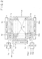
- Fig. 2 is a block diagram of a detailed mechanism of the LCD panel 10 in Fig. 1, and the same references as in Fig. 1 denote the same functional blocks.
- Reference 11a denotes a switch group for a video signal reversed for each line via a reversing amplifier 11b, which switch group are sequentially closed in clock timing of the X shift register 11.
- a pixel signal for display is supplied to each data bus line via an analog switch formed by a transfer gate.
- Reference 12 denotes a Y shift register that starts in timing of the vertical synchronizing signal Vst and is formed by unit registers equal in number to that of horizontal lines.
- the Y shift register distributes a signal to turn on a gate electrode of a transistor TFT for each pixel in timing of V CLK for scanning the horizontal lines on a display plane.
- the precharge voltage supplied via a switch 13b is supplied from a switch group 13a to data bus line electrodes in timing of the clock PCGclk of the PCG shift register 13.
- a PCG select signal PCGsel selects between the precharge signals of different voltages so as to correspond to the polarity of the video signal to be written.
- the other electrode plane of the liquid crystal panel formed by opposite electrodes is supplied with a common voltage Vcom, which corresponds to an average direct-current level of an alternating-current signal.
- the common voltage Vcom is adjusted for each LCD panel so as to be balanced with the alternating-current signal.
- a video pattern of the Vcom voltage at the time of adjustment can be made for each LCD panel by a signal pattern formed by field reversal and line reversal and by a video pattern formed by line reversal and also dot line reversal, in which adjacent pixel signals are opposite to each other in polarity in a horizontal direction.
- Fig. 3 indicates polarity of each pixel signal in carrying out a line reversal driving method with + or -, and shows parts of the pixels of the R color, G color, and B color panels from the left.
- Fig. 3 shows, in a vertical direction, that the signal polarity of each panel will be reversed in the next field.
- the G color panel which has the greatest luminance variation in frame cycles, is driven in polarity opposite from the signal polarity of the other R color and B color panels.
- the R color and B color signals are controlled to be of opposite polarity from that of G color light, which governs about 60% of the brightness.
- Such a reversal method renders luminance variation in each field less noticeable in spatial terms.
- the display screen adjusting method according to the present technique has a second adjusting operation for finely adjusting a common voltage Vcom•B for only the B color, for example, in addition to the operation of adjusting the common voltage Vcom of each of the LCD panels as described above.
- the common voltage Vcom of each of the LCD panels is first roughly adjusted in such a manner that each of the LCD panels has least luminance variation in field cycles.
- an image modulated and synthesized by the LCD panels is projected on a screen or the like to make the second adjustment.
- the second adjustment is made on the LCD panel 10B that has minimized B color luminance variation in each field by reversal driving for only the B color, and therefore may consequently unbalance the common voltage Vcom•B of the B color.
- the adjustment can be made so that flicker, which is noticeable especially on a large bright screen and cannot be removed completely by a conventional Vcom adjusting operation, is further reduced to luminance variation below a detection limit.
- Figs. 4A and 4B show waveforms obtained by measuring the luminance variation of the R, G, and B LCD panels driven by the above-mentioned reversal driving method on a time axis with a field cycle T.
- Luminance change is observed in order of decreasing visibility, or order of G, R, and B, and their combined luminance change is shown as white light W.
- Fig. 4A shows a case of in-phase reversal driving of the R, G, and B colors.
- the combined luminance variation is obtained by adding the luminance changes of the colors together.
- the luminance variation when a halftone gray signal, which makes flicker most noticeable, is supplied is still present in each field, and thus flicker is made noticeable.
- polarity reversing control is effected such that an R color signal and a B color signal have a negative polarity when a G color signal for the same pixel has a positive polarity.
- the present technique performs such reversal driving and then readjusts Vcom of the B color LCD panel on a white screen indicating the synthetic image. Adjustment is thus made on the white synthetic screen to further reduce the luminance variation in each field.
- the blue color Vcom adjustment is added as the second fine adjustment operation. This is based on the premise that the blue color has the lowest visibility and is the least noticeable as flicker (the detection limit of its luminance variation is low).
- the Vcom voltage adjustment as final adjustment operation is not limited to the B color; the Vcom voltage of the R color may be adjusted, or both the B color and the R color may be set as colors for adjustment. Since the G color has a very high visibility, however, the Vcom fine adjustment of the G color LCD panel is not desirable.
- a pattern in which white and black are repeated in every two pixels is used for adjustment as a luminance variation adjusting pattern to eliminate a canceling effect of line reversal.
- an imbalance due to line reversal occurs, and therefore when adjustment is made by using a total white signal gray scale including the effect of line reversal so as to minimize luminance variation in a frame cycle, the luminance variation can be further reduced.
- the FRP signal for reversing signal polarity is generally outputted from a timing generator according to a vertical synchronizing signal and a horizontal synchronizing signal
- the PCGsel signal for selecting between the precharge voltages PCG1 and PCG2 is outputted to the switch circuit in synchronized relation to the FRP signal to increase writing speed.
Landscapes
- Engineering & Computer Science (AREA)
- Multimedia (AREA)
- Signal Processing (AREA)
- Liquid Crystal Display Device Control (AREA)
- Liquid Crystal (AREA)
- Transforming Electric Information Into Light Information (AREA)
- Video Image Reproduction Devices For Color Tv Systems (AREA)
- Control Of Indicators Other Than Cathode Ray Tubes (AREA)
Abstract
Description
Claims (8)
- An adjusting method for a liquid crystal projector, said liquid crystal projector having a plurality of liquid crystal panels for forming a display frame by spatially combining pieces of light modulated by said plurality of liquid crystal panels with each other, said adjusting method comprising the steps of:driving each of said liquid crystal panels by an adjusting pattern signal whose polarity is reversed in each frame, and adjusting a direct-current level of said adjusting pattern signal to average light projected by each of said liquid crystal panels in each field cycle; andthereafter adjusting the direct-current level of the adjusting pattern signal of a part of said plurality of liquid crystal panels to temporally average luminance variation of a synthetic image formed by spatially combining the pieces of light modulated by said liquid crystal panels with each other.
- An adjusting method for a liquid crystal projector as claimed in claim 1, wherein said plurality of liquid crystal panels are arranged so as to transmit R color, G color, and B color, and said part of the liquid crystal panels is for the B color.
- An adjusting method for a liquid crystal projector as claimed in claim 1, wherein said plurality of liquid crystal panels are arranged so as to transmit R color, G color, and B color, and said part of the liquid crystal panels is for the R color.
- An adjusting method for a liquid crystal projector as claimed in claim 1 or 2, wherein said adjusting pattern signal is a line-reversal alternating-current signal that is reversed in polarity in each horizontal line of a display screen or a dot-reversal alternating-current signal that is reversed in polarity in each pixel in a horizontal direction.
- An adjusting method for a liquid crystal projector as claimed in claim 1, 2, or 3, wherein the adjusting pattern signals of said liquid crystal panels are formed such that the adjusting pattern signal applied to the liquid crystal panel for G color is opposite in polarity to the adjusting pattern signals applied to the liquid crystal panel for B color and the liquid crystal panel for R color, respectively.
- A liquid crystal projector with a plurality of liquid crystal panels for forming a display frame by spatially combining pieces of light modulated by said plurality of liquid crystal panels with each other, said liquid crystal projector comprising:wherein said direct-current voltage levels of said plurality of liquid crystal panels except a part of the liquid crystal panels are adjusted so that luminance variation of light modulated in a frame cycle by the liquid crystal panels is minimized; anda driving circuit for at least supplying each of said liquid crystal panels with a display signal whose polarity is alternately reversed in each line; andan adjusting means for adjusting a direct-current voltage level of said display signal supplied to each of said liquid crystal panels by said driving circuit;
said direct-current voltage level applied to said part of the liquid crystal panels is adjusted so that luminance variation in a frame cycle of projection light modulated and synthesized by said plurality of liquid crystal panels is minimized. - A liquid crystal projector as claimed in claim 6, wherein said plurality of liquid crystal panels are for R color, G color, and B color, and said part of the liquid crystal panels is for the B color or the R color.
- A liquid crystal projector as claimed in claim 6 or 7, wherein polarity of said display signal applied to G color liquid crystal is opposite in phase to that of the signals applied to R color liquid crystal and B color liquid crystal.
Applications Claiming Priority (2)
| Application Number | Priority Date | Filing Date | Title |
|---|---|---|---|
| JP2000235252 | 2000-07-31 | ||
| JP2000235252A JP4240779B2 (en) | 2000-07-31 | 2000-07-31 | LCD projector and adjustment method |
Publications (3)
| Publication Number | Publication Date |
|---|---|
| EP1178690A2 true EP1178690A2 (en) | 2002-02-06 |
| EP1178690A3 EP1178690A3 (en) | 2004-09-29 |
| EP1178690B1 EP1178690B1 (en) | 2007-02-14 |
Family
ID=18727494
Family Applications (1)
| Application Number | Title | Priority Date | Filing Date |
|---|---|---|---|
| EP01306387A Expired - Lifetime EP1178690B1 (en) | 2000-07-31 | 2001-07-25 | Liquid crystal projector and adjusting method thereof |
Country Status (5)
| Country | Link |
|---|---|
| US (1) | US6646628B2 (en) |
| EP (1) | EP1178690B1 (en) |
| JP (1) | JP4240779B2 (en) |
| DE (1) | DE60126537T2 (en) |
| ES (1) | ES2278691T3 (en) |
Cited By (1)
| Publication number | Priority date | Publication date | Assignee | Title |
|---|---|---|---|---|
| CN108022565A (en) * | 2016-11-02 | 2018-05-11 | 群创光电股份有限公司 | adjusting method and display |
Families Citing this family (46)
| Publication number | Priority date | Publication date | Assignee | Title |
|---|---|---|---|---|
| JP4271414B2 (en) * | 2001-09-25 | 2009-06-03 | シャープ株式会社 | Image display device and display driving method |
| KR100421053B1 (en) * | 2002-02-22 | 2004-03-04 | 삼성전자주식회사 | Precharge Method and Precharge voltage generation circuit of signal line |
| US7338433B2 (en) | 2002-08-13 | 2008-03-04 | Allergan, Inc. | Remotely adjustable gastric banding method |
| BR0306183A (en) | 2002-08-28 | 2004-10-19 | Inamed Medical Products Corp | Fatigue Resistant Gastric Banding Device |
| CN100401042C (en) * | 2003-01-24 | 2008-07-09 | 牧德科技股份有限公司 | Detection method and system for liquid crystal display panel |
| JP4007239B2 (en) * | 2003-04-08 | 2007-11-14 | ソニー株式会社 | Display device |
| TWI302625B (en) * | 2003-06-26 | 2008-11-01 | Au Optronics Corp | Polysilicon thin film transistor liquid crystal display having a plurality of common voltage drivers |
| TWI230310B (en) * | 2003-12-02 | 2005-04-01 | Vxis Technology Corp | A system and a method to reduce flicker on thin film transistor liquid crystal display (TFT-LCD) |
| AU2005208721B2 (en) | 2004-01-23 | 2010-09-23 | Boston Scientific Scimed, Inc. | Releasably-securable one-piece adjustable gastric band |
| JP2005221569A (en) * | 2004-02-03 | 2005-08-18 | Seiko Epson Corp | Adjustment of the counter electrode voltage input to the LCD panel |
| DK1725193T3 (en) | 2004-03-08 | 2009-11-30 | Allergan Medical S A | Closing system for tubular members |
| JP4053508B2 (en) * | 2004-03-10 | 2008-02-27 | シャープ株式会社 | Display device driving method and display device |
| ATE517652T1 (en) | 2004-03-18 | 2011-08-15 | Allergan Inc | DEVICE FOR ADJUSTING THE VOLUME OF INTRAGASTRAL BALLOONS |
| US7986296B2 (en) | 2004-05-24 | 2011-07-26 | Au Optronics Corporation | Liquid crystal display and its driving method |
| US20060028418A1 (en) * | 2004-08-09 | 2006-02-09 | Chunghwa Picture Tubes, Ltd. | Method of pre-charge scanning for TFT-LCD panel |
| US8251888B2 (en) | 2005-04-13 | 2012-08-28 | Mitchell Steven Roslin | Artificial gastric valve |
| US9093041B2 (en) * | 2005-11-28 | 2015-07-28 | Honeywell International Inc. | Backlight variation compensated display |
| US7798954B2 (en) | 2006-01-04 | 2010-09-21 | Allergan, Inc. | Hydraulic gastric band with collapsible reservoir |
| US8043206B2 (en) | 2006-01-04 | 2011-10-25 | Allergan, Inc. | Self-regulating gastric band with pressure data processing |
| KR100761109B1 (en) | 2006-05-19 | 2007-09-21 | 엘지전자 주식회사 | Electroluminescent display and its driving method |
| JP2007310234A (en) * | 2006-05-19 | 2007-11-29 | Nec Electronics Corp | Data line driving circuit, display device and data line driving method |
| JP4281776B2 (en) * | 2006-09-29 | 2009-06-17 | セイコーエプソン株式会社 | Electro-optical device and driving method thereof |
| US20080221027A1 (en) * | 2007-03-09 | 2008-09-11 | The Regents Of The University Of California | Composition and Methods for the Treatment of Duchene Muscular Dystrophy |
| US7880711B1 (en) * | 2007-04-30 | 2011-02-01 | Lockheed Martin Corporation | Image stability in liquid crystal displays |
| CN101772800B (en) * | 2007-08-02 | 2013-01-02 | 夏普株式会社 | Liquid crystal display device and method and circuit for driving the same |
| US8317677B2 (en) | 2008-10-06 | 2012-11-27 | Allergan, Inc. | Mechanical gastric band with cushions |
| US20100185049A1 (en) | 2008-10-22 | 2010-07-22 | Allergan, Inc. | Dome and screw valves for remotely adjustable gastric banding systems |
| KR101521660B1 (en) * | 2008-12-24 | 2015-05-20 | 엘지디스플레이 주식회사 | Liquid crystal lens device |
| US8614721B2 (en) | 2009-08-28 | 2013-12-24 | Sharp Kabushiki Kaisha | Liquid crystal display device and potential setting method for the same |
| US8758221B2 (en) | 2010-02-24 | 2014-06-24 | Apollo Endosurgery, Inc. | Source reservoir with potential energy for remotely adjustable gastric banding system |
| US8840541B2 (en) | 2010-02-25 | 2014-09-23 | Apollo Endosurgery, Inc. | Pressure sensing gastric banding system |
| US9028394B2 (en) | 2010-04-29 | 2015-05-12 | Apollo Endosurgery, Inc. | Self-adjusting mechanical gastric band |
| US20110270024A1 (en) | 2010-04-29 | 2011-11-03 | Allergan, Inc. | Self-adjusting gastric band having various compliant components |
| US9044298B2 (en) | 2010-04-29 | 2015-06-02 | Apollo Endosurgery, Inc. | Self-adjusting gastric band |
| US20110270025A1 (en) | 2010-04-30 | 2011-11-03 | Allergan, Inc. | Remotely powered remotely adjustable gastric band system |
| US8517915B2 (en) | 2010-06-10 | 2013-08-27 | Allergan, Inc. | Remotely adjustable gastric banding system |
| US20120059216A1 (en) | 2010-09-07 | 2012-03-08 | Allergan, Inc. | Remotely adjustable gastric banding system |
| US8961393B2 (en) | 2010-11-15 | 2015-02-24 | Apollo Endosurgery, Inc. | Gastric band devices and drive systems |
| US8876694B2 (en) | 2011-12-07 | 2014-11-04 | Apollo Endosurgery, Inc. | Tube connector with a guiding tip |
| US8961394B2 (en) | 2011-12-20 | 2015-02-24 | Apollo Endosurgery, Inc. | Self-sealing fluid joint for use with a gastric band |
| JP5947925B2 (en) * | 2014-02-12 | 2016-07-06 | キヤノン株式会社 | ELECTRIC DEVICE, IMAGE PROJECTION DEVICE, AND IMAGING DEVICE |
| CN104680961B (en) * | 2015-03-18 | 2017-05-24 | 京东方科技集团股份有限公司 | Image detection method, image detection device, display panel and display device |
| CN106683603B (en) * | 2017-01-10 | 2019-08-06 | Oppo广东移动通信有限公司 | A kind of splashette processing method and terminal |
| CN109584834B (en) * | 2019-01-22 | 2020-05-12 | 深圳市华星光电技术有限公司 | Liquid crystal display device having a plurality of pixel electrodes |
| US11847988B2 (en) * | 2019-08-02 | 2023-12-19 | Sitronix Technology Corporation | Driving method for flicker suppression of display panel and driving circuit thereof |
| CN113626042A (en) * | 2021-07-16 | 2021-11-09 | 江西联创(万年)电子有限公司 | Method and device for burning Flicker on display screen, computer and readable storage medium |
Family Cites Families (8)
| Publication number | Priority date | Publication date | Assignee | Title |
|---|---|---|---|---|
| JPH079507B2 (en) * | 1988-07-25 | 1995-02-01 | 松下電器産業株式会社 | Liquid crystal display |
| US5041823A (en) * | 1988-12-29 | 1991-08-20 | Honeywell Inc. | Flicker-free liquid crystal display driver system |
| US5751261A (en) * | 1990-12-31 | 1998-05-12 | Kopin Corporation | Control system for display panels |
| US5731796A (en) * | 1992-10-15 | 1998-03-24 | Hitachi, Ltd. | Liquid crystal display driving method/driving circuit capable of being driven with equal voltages |
| US5905540A (en) * | 1994-12-27 | 1999-05-18 | Seiko Epson Corporation | Projection-type display apparatus |
| US6366271B1 (en) * | 1997-11-13 | 2002-04-02 | Mitsubishi Denki Kabushiki Kaisha | Method for driving a liquid crystal display apparatus and driving circuit therefor |
| JP4189062B2 (en) * | 1998-07-06 | 2008-12-03 | セイコーエプソン株式会社 | Electronics |
| US6217174B1 (en) * | 1999-01-28 | 2001-04-17 | Richard M. Knox | Image projection |
-
2000
- 2000-07-31 JP JP2000235252A patent/JP4240779B2/en not_active Expired - Fee Related
-
2001
- 2001-07-25 DE DE60126537T patent/DE60126537T2/en not_active Expired - Lifetime
- 2001-07-25 ES ES01306387T patent/ES2278691T3/en not_active Expired - Lifetime
- 2001-07-25 EP EP01306387A patent/EP1178690B1/en not_active Expired - Lifetime
- 2001-07-30 US US09/919,212 patent/US6646628B2/en not_active Expired - Fee Related
Cited By (2)
| Publication number | Priority date | Publication date | Assignee | Title |
|---|---|---|---|---|
| CN108022565A (en) * | 2016-11-02 | 2018-05-11 | 群创光电股份有限公司 | adjusting method and display |
| CN108022565B (en) * | 2016-11-02 | 2021-03-30 | 群创光电股份有限公司 | Adjusting method and display |
Also Published As
| Publication number | Publication date |
|---|---|
| JP4240779B2 (en) | 2009-03-18 |
| DE60126537D1 (en) | 2007-03-29 |
| EP1178690A3 (en) | 2004-09-29 |
| US20020011984A1 (en) | 2002-01-31 |
| DE60126537T2 (en) | 2008-02-07 |
| US6646628B2 (en) | 2003-11-11 |
| EP1178690B1 (en) | 2007-02-14 |
| JP2002049020A (en) | 2002-02-15 |
| ES2278691T3 (en) | 2007-08-16 |
Similar Documents
| Publication | Publication Date | Title |
|---|---|---|
| EP1178690B1 (en) | Liquid crystal projector and adjusting method thereof | |
| KR100375806B1 (en) | Apparatus of correcting color speck and apparatus of correcting luminance speck | |
| JP3956337B2 (en) | Frame sequential color display | |
| US7365729B2 (en) | Field sequential LCD device and color image display method thereof | |
| EP0715799B1 (en) | Display device | |
| EP1562171A2 (en) | Apparatus for adjusting the voltage of the opposed electrodes in liquid crystal panel | |
| JPS61102892A (en) | Projecting type display device | |
| CN101299323B (en) | Liquid crystal display device | |
| JP3618941B2 (en) | Driving method of display device | |
| KR100950517B1 (en) | LCD panel and driving method thereof | |
| JP2000098343A (en) | Color unevenness correction device | |
| JPS6041086A (en) | Liquid crystal color projection apparatus | |
| JP2005195832A (en) | Image display device and image display method | |
| JP2722817B2 (en) | Projection display device | |
| JP2021026195A (en) | Projection type display device | |
| JP3829479B2 (en) | Display device and driving method thereof | |
| JPH0335290A (en) | Method for driving active matrix liquid crystal display | |
| JP2000221948A (en) | Color unevenness correction device | |
| JP2015087441A (en) | Electro-optical device and driving method of electro-optical device | |
| JPH11281951A (en) | Display device driving method and display device | |
| JP3602395B2 (en) | Projection type display device | |
| EP0400993A2 (en) | Projection-type image display apparatus | |
| JP2004325916A (en) | Projection display device | |
| JP2021081666A (en) | Projection display device | |
| JP2000056737A (en) | LCD panel brightness unevenness correction device |
Legal Events
| Date | Code | Title | Description |
|---|---|---|---|
| PUAI | Public reference made under article 153(3) epc to a published international application that has entered the european phase |
Free format text: ORIGINAL CODE: 0009012 |
|
| AK | Designated contracting states |
Kind code of ref document: A2 Designated state(s): AT BE CH CY DE DK ES FI FR GB GR IE IT LI LU MC NL PT SE TR |
|
| AX | Request for extension of the european patent |
Free format text: AL;LT;LV;MK;RO;SI |
|
| PUAL | Search report despatched |
Free format text: ORIGINAL CODE: 0009013 |
|
| AK | Designated contracting states |
Kind code of ref document: A3 Designated state(s): AT BE CH CY DE DK ES FI FR GB GR IE IT LI LU MC NL PT SE TR |
|
| AX | Request for extension of the european patent |
Extension state: AL LT LV MK RO SI |
|
| 17P | Request for examination filed |
Effective date: 20050311 |
|
| AKX | Designation fees paid |
Designated state(s): DE ES FR GB |
|
| 17Q | First examination report despatched |
Effective date: 20050606 |
|
| GRAP | Despatch of communication of intention to grant a patent |
Free format text: ORIGINAL CODE: EPIDOSNIGR1 |
|
| GRAS | Grant fee paid |
Free format text: ORIGINAL CODE: EPIDOSNIGR3 |
|
| GRAA | (expected) grant |
Free format text: ORIGINAL CODE: 0009210 |
|
| AK | Designated contracting states |
Kind code of ref document: B1 Designated state(s): DE ES FR GB |
|
| REG | Reference to a national code |
Ref country code: GB Ref legal event code: FG4D |
|
| RIN1 | Information on inventor provided before grant (corrected) |
Inventor name: SHIROCHI, YOSHIKIC/O I. P. D. SONY CORPORATION Inventor name: NAGATA, YUJIC/O I. P. D. SONY CORPORATION Inventor name: ENDO, HIROAKIC/O I. P. D. SONY CORPORATION |
|
| REF | Corresponds to: |
Ref document number: 60126537 Country of ref document: DE Date of ref document: 20070329 Kind code of ref document: P |
|
| ET | Fr: translation filed | ||
| REG | Reference to a national code |
Ref country code: ES Ref legal event code: FG2A Ref document number: 2278691 Country of ref document: ES Kind code of ref document: T3 |
|
| PLBE | No opposition filed within time limit |
Free format text: ORIGINAL CODE: 0009261 |
|
| STAA | Information on the status of an ep patent application or granted ep patent |
Free format text: STATUS: NO OPPOSITION FILED WITHIN TIME LIMIT |
|
| 26N | No opposition filed |
Effective date: 20071115 |
|
| REG | Reference to a national code |
Ref country code: GB Ref legal event code: 746 Effective date: 20091130 |
|
| PGFP | Annual fee paid to national office [announced via postgrant information from national office to epo] |
Ref country code: FR Payment date: 20110729 Year of fee payment: 11 |
|
| PGFP | Annual fee paid to national office [announced via postgrant information from national office to epo] |
Ref country code: ES Payment date: 20110719 Year of fee payment: 11 Ref country code: DE Payment date: 20110722 Year of fee payment: 11 Ref country code: GB Payment date: 20110721 Year of fee payment: 11 |
|
| GBPC | Gb: european patent ceased through non-payment of renewal fee |
Effective date: 20120725 |
|
| REG | Reference to a national code |
Ref country code: FR Ref legal event code: ST Effective date: 20130329 |
|
| PG25 | Lapsed in a contracting state [announced via postgrant information from national office to epo] |
Ref country code: FR Free format text: LAPSE BECAUSE OF NON-PAYMENT OF DUE FEES Effective date: 20120731 Ref country code: GB Free format text: LAPSE BECAUSE OF NON-PAYMENT OF DUE FEES Effective date: 20120725 Ref country code: DE Free format text: LAPSE BECAUSE OF NON-PAYMENT OF DUE FEES Effective date: 20130201 |
|
| REG | Reference to a national code |
Ref country code: DE Ref legal event code: R119 Ref document number: 60126537 Country of ref document: DE Effective date: 20130201 |
|
| REG | Reference to a national code |
Ref country code: ES Ref legal event code: FD2A Effective date: 20131021 |
|
| PG25 | Lapsed in a contracting state [announced via postgrant information from national office to epo] |
Ref country code: ES Free format text: LAPSE BECAUSE OF NON-PAYMENT OF DUE FEES Effective date: 20120726 |