EP1178544A2 - Semiconductor light emitting device and method for manufacturing same - Google Patents
Semiconductor light emitting device and method for manufacturing same Download PDFInfo
- Publication number
- EP1178544A2 EP1178544A2 EP01117754A EP01117754A EP1178544A2 EP 1178544 A2 EP1178544 A2 EP 1178544A2 EP 01117754 A EP01117754 A EP 01117754A EP 01117754 A EP01117754 A EP 01117754A EP 1178544 A2 EP1178544 A2 EP 1178544A2
- Authority
- EP
- European Patent Office
- Prior art keywords
- light emitting
- semiconductor light
- diffuser
- emitting device
- fluorescent material
- Prior art date
- Legal status (The legal status is an assumption and is not a legal conclusion. Google has not performed a legal analysis and makes no representation as to the accuracy of the status listed.)
- Withdrawn
Links
Images







Classifications
-
- H—ELECTRICITY
- H10—SEMICONDUCTOR DEVICES; ELECTRIC SOLID-STATE DEVICES NOT OTHERWISE PROVIDED FOR
- H10H—INORGANIC LIGHT-EMITTING SEMICONDUCTOR DEVICES HAVING POTENTIAL BARRIERS
- H10H20/00—Individual inorganic light-emitting semiconductor devices having potential barriers, e.g. light-emitting diodes [LED]
- H10H20/80—Constructional details
- H10H20/85—Packages
- H10H20/851—Wavelength conversion means
- H10H20/8511—Wavelength conversion means characterised by their material, e.g. binder
-
- H—ELECTRICITY
- H10—SEMICONDUCTOR DEVICES; ELECTRIC SOLID-STATE DEVICES NOT OTHERWISE PROVIDED FOR
- H10H—INORGANIC LIGHT-EMITTING SEMICONDUCTOR DEVICES HAVING POTENTIAL BARRIERS
- H10H20/00—Individual inorganic light-emitting semiconductor devices having potential barriers, e.g. light-emitting diodes [LED]
- H10H20/80—Constructional details
- H10H20/85—Packages
- H10H20/852—Encapsulations
- H10H20/853—Encapsulations characterised by their shape
-
- H—ELECTRICITY
- H10—SEMICONDUCTOR DEVICES; ELECTRIC SOLID-STATE DEVICES NOT OTHERWISE PROVIDED FOR
- H10H—INORGANIC LIGHT-EMITTING SEMICONDUCTOR DEVICES HAVING POTENTIAL BARRIERS
- H10H20/00—Individual inorganic light-emitting semiconductor devices having potential barriers, e.g. light-emitting diodes [LED]
- H10H20/80—Constructional details
- H10H20/85—Packages
- H10H20/852—Encapsulations
- H10H20/854—Encapsulations characterised by their material, e.g. epoxy or silicone resins
-
- H—ELECTRICITY
- H10—SEMICONDUCTOR DEVICES; ELECTRIC SOLID-STATE DEVICES NOT OTHERWISE PROVIDED FOR
- H10H—INORGANIC LIGHT-EMITTING SEMICONDUCTOR DEVICES HAVING POTENTIAL BARRIERS
- H10H20/00—Individual inorganic light-emitting semiconductor devices having potential barriers, e.g. light-emitting diodes [LED]
- H10H20/80—Constructional details
- H10H20/882—Scattering means
-
- H—ELECTRICITY
- H10—SEMICONDUCTOR DEVICES; ELECTRIC SOLID-STATE DEVICES NOT OTHERWISE PROVIDED FOR
- H10W—GENERIC PACKAGES, INTERCONNECTIONS, CONNECTORS OR OTHER CONSTRUCTIONAL DETAILS OF DEVICES COVERED BY CLASS H10
- H10W72/00—Interconnections or connectors in packages
- H10W72/01—Manufacture or treatment
- H10W72/015—Manufacture or treatment of bond wires
- H10W72/01515—Forming coatings
-
- H—ELECTRICITY
- H10—SEMICONDUCTOR DEVICES; ELECTRIC SOLID-STATE DEVICES NOT OTHERWISE PROVIDED FOR
- H10W—GENERIC PACKAGES, INTERCONNECTIONS, CONNECTORS OR OTHER CONSTRUCTIONAL DETAILS OF DEVICES COVERED BY CLASS H10
- H10W72/00—Interconnections or connectors in packages
- H10W72/01—Manufacture or treatment
- H10W72/0198—Manufacture or treatment batch processes
-
- H—ELECTRICITY
- H10—SEMICONDUCTOR DEVICES; ELECTRIC SOLID-STATE DEVICES NOT OTHERWISE PROVIDED FOR
- H10W—GENERIC PACKAGES, INTERCONNECTIONS, CONNECTORS OR OTHER CONSTRUCTIONAL DETAILS OF DEVICES COVERED BY CLASS H10
- H10W72/00—Interconnections or connectors in packages
- H10W72/071—Connecting or disconnecting
- H10W72/073—Connecting or disconnecting of die-attach connectors
-
- H—ELECTRICITY
- H10—SEMICONDUCTOR DEVICES; ELECTRIC SOLID-STATE DEVICES NOT OTHERWISE PROVIDED FOR
- H10W—GENERIC PACKAGES, INTERCONNECTIONS, CONNECTORS OR OTHER CONSTRUCTIONAL DETAILS OF DEVICES COVERED BY CLASS H10
- H10W72/00—Interconnections or connectors in packages
- H10W72/071—Connecting or disconnecting
- H10W72/075—Connecting or disconnecting of bond wires
-
- H—ELECTRICITY
- H10—SEMICONDUCTOR DEVICES; ELECTRIC SOLID-STATE DEVICES NOT OTHERWISE PROVIDED FOR
- H10W—GENERIC PACKAGES, INTERCONNECTIONS, CONNECTORS OR OTHER CONSTRUCTIONAL DETAILS OF DEVICES COVERED BY CLASS H10
- H10W72/00—Interconnections or connectors in packages
- H10W72/50—Bond wires
- H10W72/551—Materials of bond wires
- H10W72/552—Materials of bond wires comprising metals or metalloids, e.g. silver
- H10W72/5522—Materials of bond wires comprising metals or metalloids, e.g. silver comprising gold [Au]
-
- H—ELECTRICITY
- H10—SEMICONDUCTOR DEVICES; ELECTRIC SOLID-STATE DEVICES NOT OTHERWISE PROVIDED FOR
- H10W—GENERIC PACKAGES, INTERCONNECTIONS, CONNECTORS OR OTHER CONSTRUCTIONAL DETAILS OF DEVICES COVERED BY CLASS H10
- H10W72/00—Interconnections or connectors in packages
- H10W72/851—Dispositions of multiple connectors or interconnections
- H10W72/874—On different surfaces
- H10W72/884—Die-attach connectors and bond wires
-
- H—ELECTRICITY
- H10—SEMICONDUCTOR DEVICES; ELECTRIC SOLID-STATE DEVICES NOT OTHERWISE PROVIDED FOR
- H10W—GENERIC PACKAGES, INTERCONNECTIONS, CONNECTORS OR OTHER CONSTRUCTIONAL DETAILS OF DEVICES COVERED BY CLASS H10
- H10W74/00—Encapsulations, e.g. protective coatings
-
- H—ELECTRICITY
- H10—SEMICONDUCTOR DEVICES; ELECTRIC SOLID-STATE DEVICES NOT OTHERWISE PROVIDED FOR
- H10W—GENERIC PACKAGES, INTERCONNECTIONS, CONNECTORS OR OTHER CONSTRUCTIONAL DETAILS OF DEVICES COVERED BY CLASS H10
- H10W90/00—Package configurations
- H10W90/701—Package configurations characterised by the relative positions of pads or connectors relative to package parts
- H10W90/731—Package configurations characterised by the relative positions of pads or connectors relative to package parts of die-attach connectors
- H10W90/736—Package configurations characterised by the relative positions of pads or connectors relative to package parts of die-attach connectors between a chip and a stacked lead frame, conducting package substrate or heat sink
-
- H—ELECTRICITY
- H10—SEMICONDUCTOR DEVICES; ELECTRIC SOLID-STATE DEVICES NOT OTHERWISE PROVIDED FOR
- H10W—GENERIC PACKAGES, INTERCONNECTIONS, CONNECTORS OR OTHER CONSTRUCTIONAL DETAILS OF DEVICES COVERED BY CLASS H10
- H10W90/00—Package configurations
- H10W90/701—Package configurations characterised by the relative positions of pads or connectors relative to package parts
- H10W90/751—Package configurations characterised by the relative positions of pads or connectors relative to package parts of bond wires
- H10W90/756—Package configurations characterised by the relative positions of pads or connectors relative to package parts of bond wires between a chip and a stacked lead frame, conducting package substrate or heat sink
Definitions
- This invention relates to a semiconductor light emitting device and its manufacturing method, and more particularly, to a semiconductor device using a fluorescent material and its manufacturing method.
- Light emitting devices combining a semiconductor light emitting element like LED (light emitting diode) and a fluorescent material are remarked as inexpensive and long-life light emitting devices, and they are being used widely.
- semiconductor light emitting devices those for emitting white light are especially regarded hopeful for various ways of use as light emitting devices that can substitute for fluorescent lamps or as light sources of display devices.
- Semiconductor white light emitting devices use a structure combining a semiconductor light emitting element for emission of blue light or ultraviolet light (UV emission) and a fluorescent material excited by light emitted by the light emitting element.
- semiconductor white light emitting devices generally used today include those of a structure combining a semiconductor blue light emitting element made of GaN semiconductors and a YAG fluorescent material.
- Semiconductor white light emitting devices of this type realize white light by color mixture obtained from blue emission spectrums near the center wavelength of 450 [nm] from light emitting elements and broad spectrums having peaks near the wavelength of 560 [nm] which are emitted from YAG fluorescent materials in response to emission of the light emitting elements.
- fluorescent materials are usually coated around the semiconductor light emitting element. These devices, however, are subjected to differences in thickness of fluorescent materials through which light from semiconductor light emitting elements pass, and involve the problem of variance in color tone depending on view angles.
- Semiconductor light emitting devices are often used in form of an array.
- different color tones of light emitting devices even if small, are easily visible to naked eyes, and it has been desirable that differences in color tone are minimized.
- variance in color tone is more visible, and it has been inconvenient that color tone changes depending upon view angles.
- the present invention is based on recognition of that problem. It is therefore an object of the invention to provide a semiconductor light emitting device comprising at least a semiconductor light emitting element and a fluorescent material portion including a fluorescent material excited by light from the semiconductor light emitting element and ensuring a uniform color tone.
- a semiconductor light emitting device comprising:
- a semiconductor light emitting device comprising:
- a semiconductor light emitting device comprising:
- a manufacturing method of a semiconductor light emitting device comprising:
- a manufacturing method of a semiconductor light emitting device comprising:
- the semiconductor light emitting device taken as the first embodiment is a semiconductor light emitting device for emitting white light, which is called a surface mounted device (hereinafter abbreviated as SMD).
- SMD surface mounted device
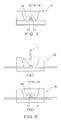
- One of features of the semiconductor light emitting device according to the instant embodiment lies in, as shown in Fig. 1, introducing an appropriate amount of diffuser 13 into silicone resin used as sealing resin 15.
- Used as a semiconductor light emitting element 11 is an element made of GaN materials and emitting ultraviolet light when a current is injected.
- Used as fluorescent materials 12 are three kinds of fluorescent materials, namely, a red fluorescent material excited by ultraviolet emission to emit red light, a green fluorescent material excited by ultraviolet emission to emit green light, and a blue fluorescent material excited by ultraviolet emission to emit blue light (hereinafter abbreviated as RGB fluorescent materials).
- RGB fluorescent materials used as the diffuser 13 is alumina (Al 2 O 3 ) powder.
- Fig. 1 is a schematic cross-sectional view of the semiconductor light emitting device according to the first embodiment.
- the semiconductor light emitting element 11 made of GaN materials and emitting ultraviolet light upon injection of a current is bonded inside a reflector of a frame 16 with an adhesive 17 such as silver paste. Both p and n electrodes of the semiconductor light emitting device 11 are connected to the frame 16 by a wire 18 of Au, for example.
- Interior of the reflector of the frame 16 is filled with silicon resin 15.
- RGB fluorescent materials 12 and diffuser 13 are mixed into the silicon resin 15.
- weight % concentration of the diffuser 13 in the silicon resin 15 is 2%.
- the silicon resin 15 is commonly used as sealing resin for covering the semiconductor light emitting element 11, fluorescent material portion including fluorescent materials 12 and diffuser portion including the diffuser 13.
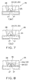
- a manufacturing method of the semiconductor light emitting device according to the first embodiment is briefly explained with reference to Figs. 2(a) and 2(b).
- the semiconductor light emitting element 11 is fixed inside the reflector of the frame 16 by using the adhesive 17 such as silver paste.
- both p and n electrodes of the semiconductor light emitting element 11 are connected to the frame 16 with a wire 17 of Au, for example.
- predetermined compounding ratios of RGB fluorescent materials 12 and alumina powder (diffuser) 13 are mixed in silicone resin that will become the sealing resin 15, and the preparation is stirred well to uniformly diffuse the fluorescent materials 12 and the diffuser 13. Then the resin undergoes evacuation to degas the resin. Degassing may be conducted in parallel with the stir.
- prepared silicone resin 15 is filled inside the reflector of the frame 16.
- thermosetting is conducted to fix the fluorescent materials 12 and the diffuser 13. Thereafter, SMD is separated from the frame, thereby to obtain the semiconductor light emitting device shown in Fig. 1. If the resin is not degassed, bubbles will remain in the cured sealing resin 15, and luminous intensity of the device will decrease.
- emission of white light can be obtained by color mixture of red light emitd from the red fluorescent material, green light emitd from the green fluorescent material and blue light emitd from the blue fluorescent material.
- the semiconductor light emitting device using the diffuser 13 as explained above with reference to Fig. 1, can uniform the intended color tone. That is, in the light emitting device of Fig. 1, since ultraviolet emission from the semiconductor light emitting element 11 is spread in various directions by the diffuser 13, the ultraviolet emission efficiently couples to the red fluorescent material, green fluorescent material and blue fluorescent material. Additionally, emission from each fluorescent material is also spread in various directions by the diffuser 13. As a result, emission from each fluorescent material 12 is uniformly mixed with light from the other fluorescent materials 12 to produce an intended color tone. That is, it is possible to obtain a light emitting device with no irregular color visible from any view angle.
- silicone resin having a high viscosity would be unlikely to permit downward movements of fluorescent materials 12, even when they are heavy. Therefore, when using silicone resin, uneven distribution of fluorescent materials 12 would be reduced in the degassing or thermosetting process. In this manner, the advantage of silicon resin, i.e. less variant distribution of fluorescent materials 12 during degassing or thermosetting, would surpass its above-mentioned disadvantages, and this would contribute to alleviating unevenness of distribution of the fluorescent materials 12.
- the semiconductor light emitting device of Fig. 1 uses the diffuser 13, it can improve the distribution of luminous intensity so as to prevent changes in luminous intensity depending on view angles.
- luminous intensity pertains to luminous flux per unit solid angle propagating in a certain direction.
- the semiconductor light emitting device of Fig. 1 can enhance the luminous intensity of the device. This should be far from expectation for a person skilled in that because it has been the general belief that light emitting devices using diffusers 13 will deteriorate in luminous intensity. This is discussed below.
- the diffuser 13 intrudes into fluorescent materials 12 and has these fluorescent materials 12 diffused uniformly, thereby to make uniform gaps among respective fluorescent materials 12.
- the fluorescent materials 12, uniformly dispersed can efficiently receive ultraviolet emission from the semiconductor light emitting element 11. As a result, emission from each fluorescent material 12 is enhanced, and luminous intensity of the device is enhanced as well.
- the fluorescent materials 12 do not disperse uniformly and an unevenness is produced in distribution of the fluorescent materials 12 to leave a part of the fluorescent materials 12 denser, it is difficult for the denser part of the fluorescent materials 12 to receive ultraviolet emission from the semiconductor light emitting element 11. As a result, emission of the dense part of the fluorescent materials 12 decreases, and luminous intensity of the device decreases as well. Results of careful review on quantity of the diffuser 13 will be explained later.
- silicone resin as the sealing resin 15 contributes to further enhancement of the luminous intensity of the device and to alleviating deterioration of the device. That is, since silicone resin 15 absorbs almost no ultraviolet emission, and does not react on ultraviolet emission, its quality is not changed by ultraviolet emission. Therefore, ultraviolet emission from the semiconductor light emitting element 11 is not absorbed by the silicone resin 15, and it excites the fluorescent materials 12 with a high efficiency. As a result, emission from the fluorescent materials 12 is enhanced, and luminous intensity of the light emitting device is enhanced as well.
- epoxy resin widely used conventionally, absorbs and reacts on ultraviolet light, and is subjected to changes such as coloring, for example. The part having changed in quality exhibits a higher absorptance to ultraviolet emission. Therefore, deterioration by ultraviolet emission is accelerated. As a result, emission luminous intensity of the device is lowered.
- the diffuser 13 is mixed into the silicone resin 15 by 2% in weight % concentration, but the quantity may be changed as discussed below.
- Fig. 3 is a diagram that shows changes of luminous intensity of the semiconductor device of Fig. 1 with changes in quantity of the diffuser 13 mixed into the silicone resin 15.
- the abscissa indicates weight % concentration of the diffuser 13 relative to the silicone resin 15.
- Points S each indicate total luminous flux ⁇ resulting from integration of the quantity of light emitted from the semiconductor light emitting device, and the ordinate indicates ratios of total luminous flux ⁇ relative to total luminous flux ⁇ obtained without mixing the diffuser 13.
- Points L each indicate luminous intensity I v in the front direction of the semiconductor light emitting device, and the ordinate indicates ratios of luminous intensity I v relative to luminous intensity I v obtained without mixing the diffuser 13.
- both the total luminous flux ratio S and the luminous intensity ratio L increase.
- the quantity of the diffuser 13 is 2.0%, both the total luminous flux ratio S and the luminous intensity ratio L are about 1.08 to 1.09. That is, by mixing the diffuser 13 into the silicon resin 15 by the ratio of 2.0%, both the total luminous flux ⁇ and the front luminous intensity I v are raised.
- quantity of the diffuser 13 is preferably at least 0.5%, and more preferably at least 1%.
- the diffuser 13 As reviewed above, if the diffuser 13 is excessively increased, it cannot be stirred sufficiently in the silicone resin 15, and color tone and luminous intensity vary largely among devices. In Inventor's experiments, in order to minimize fluctuation in color tone and luminous intensity, it was preferable to limit the quantity of the diffuser 13 to or below 5.0%, and more preferably to or below 2.5%.
- quantity of the diffuser 13 mixed into the silicone resin 15 should be in the range from 0.5% to 5.0% in weight % concentration, preferably in the range from 1.0% to 2.5%, and more preferably 2.0% approximately.
- a semiconductor light emitting device comprises, as shown in Fig. 5, a sealing resin 25, a binder 24 in which fluorescent materials 22 and a diffuser 23 are mixed, which are formed as separate elements. Configuration of the product, kind of the semiconductor light emitting element 21, kinds of the fluorescent materials 22 and kind of the diffuser 23 are the same as those of the first embodiment.
- Fig. 5 is a schematic cross-sectional view of the semiconductor light emitting device according to the second embodiment.
- the semiconductor light emitting element 21 made of GaN materials and emitting ultraviolet light upon injection of a current is bonded inside a reflector of a frame 26 with an adhesive 27 such as silver paste. Both p and n electrodes of the semiconductor light emitting device 21 are connected to the frame 26 by a wire 28 of Au, for example.
- a lower portion inside the reflector of the frame 26 in the view of Fig. 5 is filled with a binder (contact-assist material, dipping material, coat material or potting material) 24.
- RGB fluorescent materials 22 and diffuser 23 are mixed into the binder 24.
- the binder 24 is commonly used as fluorescent material portion including fluorescent materials 22 and diffuser portion including the diffuser 23.
- the portion above the binder 24, when viewed in Fig. 5, is filled with sealing resin 25.
- the semiconductor light emitting element 21 is fixed inside the reflector of the frame 26 by using the adhesive 27 such as silver paste.
- both p and n electrodes of the semiconductor light emitting element 21 are connected to the frame 26 with a wire 28.
- predetermined compounding ratios of RGB fluorescent materials 22 and alumina powder (diffuser) 23 are mixed in the binder 24, and the preparation is stirred well to uniformly diffuse the fluorescent materials 22 and the diffuser 23.
- the prepared binder 24 is filled in the lower portion inside the reflector of the frame 26 when viewed in the figure.
- thermosetting is conducted to fix the fluorescent materials 22 and the diffuser 23.
- the sealing resin 25 is filled in the upper portion inside the reflector of the frame 26.
- the sealing resin 25 is cured.
- emission of white light can be obtained by color mixture of red light emitted from the red fluorescent material, green light emitted from the green fluorescent material and blue light emitted from the blue fluorescent material.
- the semiconductor light emitting device using the diffuser 23 as explained above with reference to Fig. 5, can uniform the color tone similarly to the first embodiment (Fig. 1).
- the red fluorescent material when the red fluorescent material is the heaviest, the red fluorescent material gathers in the lower portion. As a result, light from the semiconductor light emitting element first passes through the red fluorescent material portion abundant in red fluorescent material. Therefore, when viewed from the front face of the light emitting device, thickness of the red fluorescent material portion the light from the light emitting element pass through is thinned, and the color tone becomes closer to blue or green. To the contrary, when the light emitting device is viewed from an angle deviated toward the side wall, the red fluorescent material portion the light from the light emitting element passes through becomes thicker, and the color tone approaches red.
- the color tone can be uniformed. That is, in the light emitting device shown here, since ultraviolet emission from the semiconductor light emitting element 21, red, green and blue emission from the fluorescent materials 22 are spread in various directions inside the reflector of the frame 26 by the diffuser 23, extracted light can be regarded as an even light source departing from the top surface of the binder 24, and the color tone is uniformed. That is, a light emitting device without color irregularity from any view angle can be obtained.
- luminous intensity of the device can be increased similarly to the first embodiment (Fig. 1).
- silicone resin or other resin can be used as the binder 24.
- Figs. 7(a) and 7(b) are schematic cross-sectional views that show modifications of the second embodiment of the invention. These modifications are different from the second embodiment in shape of the binder 24 and the sealing resin 25.
- the binder 24 containing the diffuser 23 and the fluorescent materials 22 has a cylindrical shape, and the sealing resin 25 is buried around it.
- the binder 24 containing the diffuser 23 and the fluorescent materials 22 has a cylindrical shape, and the sealing resin 25 is buried on the top and around it.
- silicon resin or other resin may be used as the binder 24.
- the binder 24 and the sealing resin 25 may be shaped as the second embodiment, depending upon their materials and the way of use of the light emitting device. Also with these modifications, the same effects as those of the second embodiment can be obtained.
- a semiconductor light emitting device comprises, as shown in Fig. 8, a binder 34 in which fluorescent materials 32, an adherent or cohesive medium 33a in which a diffuser 33 is mixed, and sealing resin 35, which are formed as separate elements.
- Configuration of the product, kind of the semiconductor light emitting element 31, kinds of the fluorescent materials 32 and kind of the diffuser 33 are the same as those of the second embodiment.
- Fig. 8 is a schematic cross-sectional view of the semiconductor light emitting device according to the third embodiment.
- the semiconductor light emitting element 31 made of GaN materials and emitting ultraviolet light upon injection of a current is bonded inside a reflector of a frame 36 with an adhesive 37 such as silver paste. Both p and n electrodes of the semiconductor light emitting device 31 are connected to the frame 36 by a wire 38 of Au, for example.
- a lower portion inside the reflector of the frame 36 in the view of Fig. 8 is filled with a binder 34.
- RGB fluorescent materials 32 are mixed into the binder 34.
- the portion above the binder 34 when viewed in Fig. 8, is filled with the adherent or coherent medium 33a.
- the medium 33a contains the diffuser 33.
- the portion above the medium 33a is filled with the sealing resin 35.
- the manufacturing method recommended for manufacturing the semiconductor light emitting device of Fig. 8 is substantially the same as that explained with reference to the second embodiment (Figs. 6(a) through 6(e)), and its explanation is omitted here.
- the semiconductor light emitting device of Fig. 8, using the diffuser 33, can uniform the color tone similarly to the first embodiment (Fig. 1).
- the semiconductor light emitting device of Fig. 8 can especially alleviate uneven distribution of the diffuser 33.
- a semiconductor light emitting device comprises, as shown in Fig. 9, a binder 44 containing fluorescent materials 42, and a sealing resin 45 containing a diffuser 43, which are formed as separate elements. Configuration of the product, kind of the semiconductor light emitting element 41, kinds of the fluorescent materials 42 and kind of the diffuser 43 are the same as those of the first embodiment (Fig. 1).
- Fig. 9 is a schematic cross-sectional view of the semiconductor light emitting device according to the fourth embodiment.
- the semiconductor light emitting element 41 made of GaN materials and emitting ultraviolet light upon injection of a current is bonded inside a reflector of a frame 46 with an adhesive 47 such as silver paste. Both p and n electrodes of the semiconductor light emitting device 41 are connected to the frame 46 by a wire 48 of Au, for example.
- a lower portion inside the reflector of the frame 46 in the view of Fig. 9 is filled with a binder 44.
- RGB fluorescent materials 42 are mixed into the binder 44.
- the portion above the binder 44, when viewed in Fig. 9, is filled with the sealing resin 45.
- the diffuser is mixed into the sealing resin 45.
- the semiconductor light emitting device of Fig. 9, using the diffuser 43, can uniform the color tone similarly to the first embodiment (Fig. 1).
- the semiconductor light emitting device of Fig. 9 is different from the semiconductor light emitting device according to the third embodiment (Fig. 8) in position containing the diffuser 43, their emission patterns are slightly different, and these devices can be selectively used depending on the way of use of the lamp.
- silicone resin used in the first embodiment can be used as the sealing resin 45.
- Figs. 10(a) through 10(d) are schematic cross-sectional views that show modifications of the semiconductor light emitting device according to the fourth embodiment.
- the modifications are different from the fourth embodiment in shape of the binder 54 and the sealing resin 55.
- the binder 54 containing fluorescent materials 52 has a cylindrical shape, and the sealing resin 55 is buried on and around it.
- the binder 54 containing fluorescent materials 52 has a cylindrical shape, it is fixed by the sealing resin 55 surrounding it, and the sealing resin 55 containing the diffuser 53 is buried on it.
- the binder 54 containing fluorescent materials 52 is filled inside the reflector of the frame 56, and the sealing resin 55 containing the diffuser 53 is coated right above the reflector.
- quantity of the binder 54 containing the fluorescent materials 52 is increased whereas quantity of the sealing resin 55 containing the diffuser 53 is decreased.
- a resin can be used as the binder 54.
- the binder 54 and the sealing resin 55 may be shaped as the fourth embodiment, depending upon their materials and the way of use of the light emitting device. Also with these modifications, the same effects as those of the fourth embodiment can be obtained.
- a semiconductor light emitting device comprises, as shown in Fig. 11, a binder 64 containing a diffuser 63 and a sealing resin 65 containing fluorescent materials 62, which are formed as separate elements. Configuration of the product, kind of the semiconductor light emitting element 61, kinds of the fluorescent materials 62 and kind of the diffuser 63 are the same as those of the first embodiment (Fig. 1).
- Fig. 11 is a schematic cross-sectional view of the semiconductor light emitting device according to the fifth embodiment.
- the semiconductor light emitting element 61 made of GaN materials and emitting ultraviolet light upon injection of a current is bonded inside a reflector of a frame 66 with an adhesive 67 such as silver paste. Both p and n electrodes of the semiconductor light emitting device 61 are connected to the frame 66 by a wire 68 of Au, for example.
- the binder 64 is buried around the semiconductor light emitting element 61.
- the diffuser 63 is mixed in the binder 64.
- the space around the binder 64 is filled with the sealing resin 65.
- the sealing resin 65 contains RGB fluorescent materials 62.
- the manufacturing method recommended for manufacturing the semiconductor light emitting device of Fig. 11 is substantially the same as that explained with reference to the second embodiment (Fig. 6(a) through 6(e)), and its explanation is omitted here.
- the device according to the instant embodiment is slightly inferior to the first to fourth embodiments from the viewpoint of uniforming the color tone, but it is especially excellent in effect of enhancing the emission intensity. Its reason will be as follows. That is, when using a semiconductor light emitting element 61 for ultraviolet emission, reflectors in conventional devices were liable to partly absorb ultraviolet emission without reflecting it sufficiently. Therefore, ultraviolet emission in horizontal directions from the semiconductor light emitting element 61 was often absorbed before exciting fluorescent materials 62. In contrast, in the light emitting device of Fig. 11, using the diffuser 63, it is assumed that ultraviolet emission in horizontal directions is spread vertically by the diffuser 63, then efficiently couples to the fluorescent materials 62, and thereby enhances the emission intensity. Furthermore, since light from the fluorescent materials 62 is partly diffused by the diffuser 63, the device shown here is also effective to uniform the color tone.
- Fig. 12 is a schematic cross-sectional view of a modification of the semiconductor light emitting device according to the fifth embodiment.
- the modification is different from the fifth embodiment in shape of the binder 64 and the sealing resin 65.
- the binder 64 containing the diffuser 63 is coated substantially uniformly on the inner wall of the reflector, and the sealing resin 65 containing fluorescent materials 62 is buried above it.
- the binder 64 and the sealing resin 65 may be shaped as shown in Fig. 12, depending upon their materials and the way of use of the light emitting device. This modified device also ensures the same effects as those of the fifth embodiment.
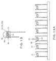
- the semiconductor light emitting device is one called LED lamp for white emission as shown in Fig. 13.
- an element made of GaN materials and emitting blue light in response to an injected current as a semiconductor light emitting element 71.
- Used as fluorescent materials 72 are YAG fluorescent materials excited by blue emission to emit yellow light.
- Used as a diffuser 73 is calcium carbonate powder. In the device of Fig. 13, the fluorescent materials 72 and the diffuser 73 are mixed in the binder 74.
- Fig. 13 is a schematic cross-sectional view of the semiconductor light emitting device according to the sixth embodiment of the invention.
- the semiconductor light emitting element 71 made of GaN materials and emitting ultraviolet light upon injection of a current is bonded inside a reflector of a frame 76 with an adhesive 77 such as silver paste. Both p and n electrodes of the semiconductor light emitting device 71 are connected to the frame 76 by a wire 78 of Au, for example.
- Interior of the reflector of the frame 76 is filled with the binder 74.
- the YAG fluorescent materials 72 and the diffuser 73 are mixed in the binder 74.
- the binder 74 is commonly used as fluorescent material portion including fluorescent materials 72 and diffuser portion including the diffuser 73.
- the semiconductor light emitting element 71 is fixed inside the reflector of each frame 76 by using the adhesive 77 such as silver paste.
- both p and n electrodes of the semiconductor light emitting element 71 are connected to the frame 76 with a wire 78.
- predetermined compounding ratios of YAG fluorescent materials 72 and calcium carbonate powder (diffuser) 73 are mixed in the binder 74, and the preparation is stirred well to uniformly diffuse the fluorescent materials 72 and the diffuser 73.
- thermosetting is conducted to fix the fluorescent materials 72 and the diffuser 73.
- Fig. 14E the sealing resin 75 is filled and cured in a case mold 79 having a configuration usable as a lens as well.
- Reference numerals already shown in Fig. 14D are omitted from Fig. 14E for easier view of the figure.
- emission of white light can be obtained by color mixture of blue light from the semiconductor light emitting element 71 and yellow light from the YAG fluorescent materials 72 excited by emission of the blue light.
- the color tone can be uniformed from any view angles. That is, in the semiconductor light emitting device of Fig. 13, since blue emission from the semiconductor light emitting element 71 and yellow light from the YAG fluorescent materials 72 can be spread in various directions inside the reflector of the frame 76, extracted light can be regarded as an even light source departing from the top surface of the reflector, and the color tone is uniformed. That is, a light emitting device without color irregularity from any view angle can be obtained.
- quantity of the fluorescent materials 72 required for obtained the same color tone as that of a device not using the diffuser 73 can be reduced. Its reason can be analyzed as follows. That is, in the semiconductor light emitting device of Fig. 13 using the diffuser 73, the blue emission from the semiconductor light emitting element 71 would be spread and efficiently couple to the YAG fluorescent materials 72 inside the reflector of the frame 76, and therefore, intensive emission from the YAG fluorescent materials 72 can be obtained.
- luminous intensity of emission can be improved as compared with devices not using the diffuser 73. Its reason is analyzed to lie in that efficient coupling of the blue emission from the semiconductor light emitting element 71 and the YAG fluorescent materials 72 makes it possible to efficiently use the blue emission from the semiconductor light emitting element 71 and the yellow emission from the YAG fluorescent materials 72.
- a semiconductor light emitting device comprises a binder 84 containing fluorescent materials 82 and a medium 83a containing a diffuser 83, which are formed as separate elements.
- Configuration of the product, kind of the semiconductor light emitting element 81, kinds of the fluorescent materials 82 and kind of the diffuser 83 are the same as those of the sixth embodiment (Fig. 13).
- Fig. 15 is a schematic cross-sectional view of the semiconductor light emitting device according to the seventh embodiment of the invention.
- the semiconductor light emitting element 81 made of GaN materials and emitting ultraviolet light upon injection of a current is bonded inside a reflector of a frame 86 with an adhesive 87 such as silver paste. Both p and n electrodes of the semiconductor light emitting device 81 are connected to the frame 86 by a wire 88 of Au, for example.
- Interior of the reflector of the frame 86 is filled with the binder 84.
- the YAG fluorescent materials 82 are mixed in the binder 84.
- the medium 83a either adherent or coherent, containing the diffuser 83 is coated. Then the sealing resin 85 covers them all.
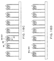
- a manufacturing method of the semiconductor light emitting device according to the seventh embodiment is explained below with reference to Figs. 16A through 16F.
- the semiconductor light emitting element 81 is fixed inside the reflector of each frame 86 by using the adhesive 87 such as silver paste.
- both p and n electrodes of the semiconductor light emitting element 81 are connected to the frame 86 with a wire 88.
- the YAG fluorescent materials 82 are introduced into the binder 84, and they are stirred well to uniformly diffuse the fluorescent materials 82. Thereafter, as shown in Fig. 16C, the prepared binder 84 is filled inside the reflector of the frame 86, and under the condition, thermosetting is conducted to fix the fluorescent materials 82.
- the diffuser 83 is introduced into the adherent or coherent medium 83a, and they are stirred well to uniformly diffuse the diffuser 83. Then, as shown in Fig. 16D, the prepared medium 83a is coated right above the reflector, and under the condition, it is dried to fix the diffuser 83. Reference numerals already shown in Fig. 16C are omitted from Fig. 16D and the next Fig. 16E for easier view of the figures.
- the sealing resin 85 is filled and cured in a case mold 89 having a configuration useable as a lens as well.
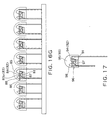
- the manufacturing method explained here can be modified by reducing the quantity of the binder 84 such that the medium 83a is limited within the reflector of the frame 86 as shown in Fig. 16G.
- emission of white light can be obtained by color mixture of blue light from the semiconductor light emitting element 81 and yellow light from the YAG fluorescent materials 82 excited by emission of the blue light.
- the semiconductor light emitting device of Fig. 15, using the diffuser 83, can uniform the color tone. That is, in the light emitting device of Fig. 15, since blue emission from the semiconductor light emitting element 81 and yellow light from the YAG fluorescent materials 82 are spread in various directions by the diffuser 83 just above the reflector of the frame 86, extracted light can be regarded as an even light source departing from the top surface of the medium 83a, and the color tone is uniformed. That is, a light emitting device without color irregularity from any view angle can be obtained.
- the binder 84 containing the fluorescent materials 82 and the medium 83a containing the diffuser 83 are prepared as separate elements, unevenness of the fluorescent materials 82 and the diffuser 83 can be minimized.
- the semiconductor light emitting device comprises a binder 94 containing fluorescent materials 92 and a sealing resin 95 containing a diffuser 93, which are formed as separate elements. Configuration of the product, kind of the semiconductor light emitting element 91, kinds of the fluorescent materials 92 and kind of the diffuser 93 are the same as those of the sixth embodiment (Fig. 13).
- Fig. 17 is a schematic cross-sectional view of the semiconductor light emitting device according to the eighth embodiment of the invention.
- the semiconductor light emitting element 91 made of GaN materials and emitting ultraviolet light upon injection of a current is bonded inside a reflector of a frame 96 with an adhesive 97 such as silver paste. Both p and n electrodes of the semiconductor light emitting device 91 are connected to the frame 96 by a wire 98 of Au, for example.
- Interior of the reflector of the frame 96 is filled with the binder 94.
- the YAG fluorescent materials 92 are mixed in the binder 94.
- the diffuser 93 is mixed in the sealing resin 95.
- the manufacturing method recommended for manufacturing the semiconductor light emitting device of Fig. 17 is substantially the same as that explained with reference to the sixth embodiment (Figs. 14A through 14E), and its explanation is omitted here.
- the semiconductor light emitting device of Fig. 17, using the diffuser 93, can uniform the color tone similarly to the seventh embodiment (Fig. 15).
- the semiconductor light emitting device of Fig. 17 and the semiconductor light emitting device according to the seventh embodiment (Fig. 15) are different in position containing the diffuser 93, their emission patterns are slightly different, and these devices can be selectively used depending on the way of use of the lamp.
- the semiconductor light emitting device is a version modified from the semiconductor light emitting device according to the first embodiment (Fig. 1) in kinds of fluorescent materials 12 and kinds of diffuser 13. More specifically, used as the fluorescent materials 12 are a blue fluorescent material excited by ultraviolet emission from the semiconductor light emitting element 11 to emit blue light, a YAG fluorescent material excited by blue emission from the blue fluorescent material to emit yellow light, and a red fluorescent material excited by ultraviolet emission from the semiconductor light emitting element 11 to emit red light. Used as the diffuser 12 is silica powder.
- emission of white light can be obtained by color mixture of red light emitd from the red fluorescent material, blue light emitd from the blue fluorescent material, and yellow light emitd from the YAG fluorescent material.
- the light emitting device according to the instant embodiment also ensured the same effects as those of the semiconductor light emitting device according to the first embodiment (Fig. 1).
- the semiconductor light emitting device is a version modified from the semiconductor light emitting device according to the fourth embodiment (Fig. 9) in kinds of fluorescent materials 42. More specifically, used as the fluorescent materials 42 are a blue fluorescent material excited by ultraviolet emission from the semiconductor light emitting element 41 to emit blue light and a YAG fluorescent material excited by the blue fluorescent material to emit yellow light.
- emission of white light can be obtained by color mixture of blue light emitd from the blue fluorescent material and yellow light emitd from the YAG fluorescent material.
- semiconductor light emitting devices using two kinds of fluorescent materials 42 as the instant embodiment does, conventional semiconductor light emitting devices not using the diffuser 43 involved the problem of changed in color tone depending on view angles for the same reason as already explained with reference to the second embodiment (Fig. 5) using three kinds of fluorescent materials 22.
- the semiconductor light emitting device according to the present embodiment can uniform the color tone by using the diffuser 43. That is, in the semiconductor light emitting device according to the instant embodiment, since blue light from the blue fluorescent material and yellow light from the YAG fluorescent material are spread in various directions inside the reflector of the frame 46, extracted light can be regarded as an even light source departing from the top surface of the reflector, and the color tone is uniformed. That is, a light emitting device without color irregularity from any view angle can be obtained.
Landscapes
- Led Device Packages (AREA)
- Led Devices (AREA)
Abstract
Description
Claims (20)
- A semiconductor light emitting device comprising:a semiconductor light emitting element which emits light of a first wavelength when a current is injected thereto; anda fluorescent material portion containing in mixture a fluorescent material and a diffuser, said fluorescent material being excited by light of the first wavelength to emit light of a second wavelength.
- The semiconductor light emitting device according to claim 1 wherein said diffuser contains at least one of calcium carbonate, silica, SiO2 and Al2O3.
- The semiconductor light emitting device according to claim 1 wherein said fluorescent material portion includes silicone resin which contains in mixture said fluorescent material and said diffuser.
- The semiconductor light emitting device according to claim 3 wherein weight % concentration of said diffuser in said fluorescent material portion is in the range from 0.5% to 5.0%.
- The semiconductor light emitting device according to claim 4 wherein weight % concentration of said diffuser in said fluorescent material portion is in the range from 1.0% to 2.5%.
- The semiconductor light emitting device according to claim 1 wherein said semiconductor light emitting element includes at least one of AlxInyGa1-x-yN (0≦x≦1, 0≦y≦1, 0≦ x+y≦1), BzGa1-zN (0≦z≦1) and SiC.
- A semiconductor light emitting device comprising:a semiconductor light emitting element which emits ultraviolet light when a current is injected thereto; anda fluorescent material portion including silicone resin which contain in mixture a blue emission fluorescent material excited by said ultraviolet light to emit blue light, a green emission fluorescent material excited by said ultraviolet light to emit green light, a red emission fluorescent material excited by said ultraviolet light to emit red light, and a diffuser.
- The semiconductor light emitting device according to claim 7 wherein said diffuser contains at least one of calcium carbonate, silica, SiO2 and Al2O3.
- The semiconductor light emitting device according to claim 8 wherein weight % concentration of said diffuser in said silicone resin is in the range from 0.5% to 5.0%
- The semiconductor light emitting device according to claim 9 wherein weight % concentration of said diffuser in said silicone resin is in the range from 1.0% to 2.5%.
- The semiconductor light emitting device according to claim 7 wherein said semiconductor light emitting element includes at least one of AlxInyGa1-x-yN (0≦x≦1, 0≦y≦1, 0≦ x+y≦1), BzGa1-zN (0≦z≦1) and SiC.
- A semiconductor light emitting device comprising:a semiconductor light emitting element which emits light of a first wavelength when a current is injected thereto;a fluorescent material portion containing in mixture a fluorescent material excited by light of the first wavelength to emit light of a second wavelength; anda diffuser portion which is a separate element from said fluorescent material portion and contains in mixture a diffuser.
- The semiconductor light emitting device according to claim 12 wherein said diffuser contains at least one of calcium carbonate, silica, SiO2 and Al2O3.
- The semiconductor light emitting device according to claim 12 wherein said diffuser is mixed in silicone resin.
- The semiconductor light emitting device according to claim 14 wherein weight % concentration of said diffuser in said diffuser portion is in the range from 0.5% to 5.0%.
- The semiconductor light emitting device according to claim 15 wherein weight % concentration of said diffuser in said diffuser portion is in the range from 1.0% to 2.5%.
- The semiconductor light emitting device according to claim 12 wherein said semiconductor light emitting element includes at least one of AlxInyGa1-x-yN (0≦x≦1, 0≦y≦1, 0≦ x+y≦1), BzGa1-zN (0≦z≦1) and SiC.
- The semiconductor light emitting device according to claim 12 wherein sealing resin disposed around said semiconductor light emitting element functions as said diffuser portion or said fluorescent material portion.
- A manufacturing method of a semiconductor light emitting device, comprising:forming a semiconductor light emitting element which emits light of a first wavelength when a current is injected thereto; andforming a fluorescent material portion which contains in mixture a fluorescent material excited by light of said first wavelength to emit light of a second wavelength, and a diffuser.
- A manufacturing method of a semiconductor light emitting device, comprising:forming a semiconductor light emitting element which emits light of a first wavelength when a current is injected thereto;forming a fluorescent material portion which contains in mixture a fluorescent material excited by light of said first wavelength to emit light of a second wavelength; andforming a diffuser portion which is a separate member from said fluorescent material portion and contains in mixture a diffuser.
Applications Claiming Priority (2)
| Application Number | Priority Date | Filing Date | Title |
|---|---|---|---|
| JP2000232050A JP2002050797A (en) | 2000-07-31 | 2000-07-31 | Semiconductor-excited phosphor light emitting device and method of manufacturing the same |
| JP2000232050 | 2000-07-31 |
Publications (2)
| Publication Number | Publication Date |
|---|---|
| EP1178544A2 true EP1178544A2 (en) | 2002-02-06 |
| EP1178544A3 EP1178544A3 (en) | 2009-02-18 |
Family
ID=18724789
Family Applications (1)
| Application Number | Title | Priority Date | Filing Date |
|---|---|---|---|
| EP01117754A Withdrawn EP1178544A3 (en) | 2000-07-31 | 2001-07-31 | Semiconductor light emitting device and method for manufacturing same |
Country Status (5)
| Country | Link |
|---|---|
| US (4) | US6576931B2 (en) |
| EP (1) | EP1178544A3 (en) |
| JP (1) | JP2002050797A (en) |
| CN (1) | CN1193438C (en) |
| TW (1) | TW535303B (en) |
Cited By (6)
| Publication number | Priority date | Publication date | Assignee | Title |
|---|---|---|---|---|
| EP1589591A2 (en) | 2004-04-23 | 2005-10-26 | Stanley Electric Co., Ltd. | Semiconductor light emitting device and method of manufacturing the same |
| WO2010035210A1 (en) * | 2008-09-24 | 2010-04-01 | Philips Lumileds Lighting Company, Llc | Led with controlled angular non-uniformity |
| EP1592074A3 (en) * | 2004-04-30 | 2010-09-08 | OSRAM Opto Semiconductors GmbH | Light emitting diode assembly |
| US8641256B2 (en) | 2007-11-06 | 2014-02-04 | Sanken Electric Co., Ltd. | Semiconductor light emitting device, composite light emitting device with arrangement of semiconductor light emitting devices, and planar light source using composite light emitting device |
| WO2014173719A1 (en) * | 2013-04-25 | 2014-10-30 | Osram Opto Semiconductors Gmbh | Optoelectronic component and method for the production thereof |
| EP2595205A3 (en) * | 2011-11-16 | 2015-12-02 | LG Innotek Co., Ltd. | Light emitting diode device |
Families Citing this family (75)
| Publication number | Priority date | Publication date | Assignee | Title |
|---|---|---|---|---|
| JP2002050797A (en) * | 2000-07-31 | 2002-02-15 | Toshiba Corp | Semiconductor-excited phosphor light emitting device and method of manufacturing the same |
| WO2003021691A1 (en) * | 2001-09-03 | 2003-03-13 | Matsushita Electric Industrial Co., Ltd. | Semiconductor light emitting device, light emitting apparatus and production method for semiconductor light emitting device |
| JP3597810B2 (en) * | 2001-10-10 | 2004-12-08 | 富士通株式会社 | Solder paste and connection structure |
| JP3939177B2 (en) * | 2002-03-20 | 2007-07-04 | シャープ株式会社 | Method for manufacturing light emitting device |
| KR100567549B1 (en) * | 2002-05-11 | 2006-04-05 | 서울반도체 주식회사 | Light-emitting diodes and their manufacturing method |
| US7928455B2 (en) * | 2002-07-15 | 2011-04-19 | Epistar Corporation | Semiconductor light-emitting device and method for forming the same |
| JP4280050B2 (en) * | 2002-10-07 | 2009-06-17 | シチズン電子株式会社 | White light emitting device |
| US6917057B2 (en) * | 2002-12-31 | 2005-07-12 | Gelcore Llc | Layered phosphor coatings for LED devices |
| EP1484802B1 (en) * | 2003-06-06 | 2018-06-13 | Stanley Electric Co., Ltd. | Optical semiconductor device |
| US7088038B2 (en) * | 2003-07-02 | 2006-08-08 | Gelcore Llc | Green phosphor for general illumination applications |
| US8999736B2 (en) * | 2003-07-04 | 2015-04-07 | Epistar Corporation | Optoelectronic system |
| US7026755B2 (en) * | 2003-08-07 | 2006-04-11 | General Electric Company | Deep red phosphor for general illumination applications |
| US6995402B2 (en) * | 2003-10-03 | 2006-02-07 | Lumileds Lighting, U.S., Llc | Integrated reflector cup for a light emitting device mount |
| US20070149496A1 (en) * | 2003-10-31 | 2007-06-28 | Jack Tuszynski | Water-soluble compound |
| JP4180537B2 (en) * | 2003-10-31 | 2008-11-12 | シャープ株式会社 | Optical element sealing structure, optical coupler, and optical element sealing method |
| CN100431181C (en) * | 2003-10-31 | 2008-11-05 | 夏普株式会社 | Sealing structure for optical element, optical coupler, and method for sealing optical element |
| JP4309242B2 (en) * | 2003-12-19 | 2009-08-05 | Necライティング株式会社 | Red phosphor material, white light emitting diode using red phosphor material, and lighting device using white light emitting diode |
| JP2005252219A (en) * | 2004-02-06 | 2005-09-15 | Toyoda Gosei Co Ltd | Light emitting device and sealing member |
| JP4516337B2 (en) * | 2004-03-25 | 2010-08-04 | シチズン電子株式会社 | Semiconductor light emitting device |
| US7517728B2 (en) * | 2004-03-31 | 2009-04-14 | Cree, Inc. | Semiconductor light emitting devices including a luminescent conversion element |
| US7514867B2 (en) | 2004-04-19 | 2009-04-07 | Panasonic Corporation | LED lamp provided with optical diffusion layer having increased thickness and method of manufacturing thereof |
| TWI398188B (en) * | 2004-08-31 | 2013-06-01 | 昭和電工股份有限公司 | A luminous body, and a lighting and display device using the luminous body |
| JP4823505B2 (en) * | 2004-10-20 | 2011-11-24 | シャープ株式会社 | Semiconductor device and electronic equipment |
| JP2006135225A (en) * | 2004-11-09 | 2006-05-25 | Toshiba Corp | Light emitting device |
| US7404652B2 (en) * | 2004-12-15 | 2008-07-29 | Avago Technologies Ecbu Ip Pte Ltd | Light-emitting diode flash module with enhanced spectral emission |
| US7473889B2 (en) * | 2004-12-16 | 2009-01-06 | Avago Technologies Ecbu Ip (Singapore) Pte. Ltd. | Optical integrated circuit package |
| TWI352437B (en) | 2007-08-27 | 2011-11-11 | Epistar Corp | Optoelectronic semiconductor device |
| US20070114562A1 (en) * | 2005-11-22 | 2007-05-24 | Gelcore, Llc | Red and yellow phosphor-converted LEDs for signal applications |
| US7358542B2 (en) * | 2005-02-02 | 2008-04-15 | Lumination Llc | Red emitting phosphor materials for use in LED and LCD applications |
| US7497973B2 (en) * | 2005-02-02 | 2009-03-03 | Lumination Llc | Red line emitting phosphor materials for use in LED applications |
| US7648649B2 (en) * | 2005-02-02 | 2010-01-19 | Lumination Llc | Red line emitting phosphors for use in led applications |
| EP1864339A4 (en) | 2005-03-11 | 2010-12-29 | Seoul Semiconductor Co Ltd | LIGHT-EMITTING DIODE DIODE WITH PHOTO-EMITTING CELL MATRIX |
| US7274045B2 (en) * | 2005-03-17 | 2007-09-25 | Lumination Llc | Borate phosphor materials for use in lighting applications |
| JP2006310771A (en) | 2005-03-30 | 2006-11-09 | Toshiba Discrete Technology Kk | Semiconductor light emitting device |
| KR100665222B1 (en) | 2005-07-26 | 2007-01-09 | 삼성전기주식회사 | LED package using diffusion material and manufacturing method thereof |
| JP2007116107A (en) * | 2005-09-22 | 2007-05-10 | Toshiba Lighting & Technology Corp | Light emitting device |
| JP5209177B2 (en) * | 2005-11-14 | 2013-06-12 | 新光電気工業株式会社 | Semiconductor device and manufacturing method of semiconductor device |
| JP2007165728A (en) * | 2005-12-15 | 2007-06-28 | Toshiba Discrete Technology Kk | Light emitting device and lighting device for visible light communication |
| JP2007180203A (en) * | 2005-12-27 | 2007-07-12 | Shinko Electric Ind Co Ltd | Semiconductor device and manufacturing method of semiconductor device |
| US8710737B2 (en) | 2006-03-28 | 2014-04-29 | Kyocera Corporation | Light-emitting device |
| JP5068472B2 (en) * | 2006-04-12 | 2012-11-07 | 昭和電工株式会社 | Method for manufacturing light emitting device |
| KR100764391B1 (en) * | 2006-04-25 | 2007-10-05 | 삼성전기주식회사 | Light emitting diode module |
| JP2006203262A (en) * | 2006-04-27 | 2006-08-03 | Kyocera Corp | Light emitting device |
| US7393065B2 (en) | 2006-06-01 | 2008-07-01 | Lockheed Martin Corporation | Redundant braking system |
| WO2008018615A1 (en) * | 2006-08-09 | 2008-02-14 | Panasonic Corporation | Light-emitting device |
| JP5334088B2 (en) | 2007-01-15 | 2013-11-06 | フューチャー ライト リミテッド ライアビリティ カンパニー | Semiconductor light emitting device |
| US9061450B2 (en) * | 2007-02-12 | 2015-06-23 | Cree, Inc. | Methods of forming packaged semiconductor light emitting devices having front contacts by compression molding |
| US7709853B2 (en) * | 2007-02-12 | 2010-05-04 | Cree, Inc. | Packaged semiconductor light emitting devices having multiple optical elements |
| US7847309B2 (en) * | 2007-07-16 | 2010-12-07 | GE Lighting Solutions, LLC | Red line emitting complex fluoride phosphors activated with Mn4+ |
| US8026533B2 (en) * | 2007-07-19 | 2011-09-27 | Nichia Corporation | Light emitting device and method of manufacturing the same |
| US11114594B2 (en) * | 2007-08-24 | 2021-09-07 | Creeled, Inc. | Light emitting device packages using light scattering particles of different size |
| US7791093B2 (en) * | 2007-09-04 | 2010-09-07 | Koninklijke Philips Electronics N.V. | LED with particles in encapsulant for increased light extraction and non-yellow off-state color |
| JP3138907U (en) * | 2007-11-06 | 2008-01-24 | サンケン電気株式会社 | Semiconductor light-emitting device, composite light-emitting device in which the semiconductor light-emitting devices are arranged, and a planar light-emitting source using the composite light-emitting device |
| TWI401820B (en) * | 2007-11-07 | 2013-07-11 | 財團法人工業技術研究院 | Light-emitting element and manufacturing method thereof |
| US8946987B2 (en) * | 2007-11-07 | 2015-02-03 | Industrial Technology Research Institute | Light emitting device and fabricating method thereof |
| US10008637B2 (en) | 2011-12-06 | 2018-06-26 | Cree, Inc. | Light emitter devices and methods with reduced dimensions and improved light output |
| US9287469B2 (en) * | 2008-05-02 | 2016-03-15 | Cree, Inc. | Encapsulation for phosphor-converted white light emitting diode |
| KR20110028307A (en) | 2008-05-29 | 2011-03-17 | 크리 인코포레이티드 | Light source with near field mixing |
| JP2010016273A (en) * | 2008-07-07 | 2010-01-21 | Sanyo Electric Co Ltd | Semiconductor light-emitting device |
| JP2010021497A (en) * | 2008-07-14 | 2010-01-28 | Sanyo Electric Co Ltd | Semiconductor light-emitting device |
| JP5245614B2 (en) * | 2008-07-29 | 2013-07-24 | 豊田合成株式会社 | Light emitting device |
| US7897419B2 (en) * | 2008-12-23 | 2011-03-01 | Cree, Inc. | Color correction for wafer level white LEDs |
| US8415692B2 (en) * | 2009-07-06 | 2013-04-09 | Cree, Inc. | LED packages with scattering particle regions |
| US8547009B2 (en) * | 2009-07-10 | 2013-10-01 | Cree, Inc. | Lighting structures including diffuser particles comprising phosphor host materials |
| JP5398657B2 (en) * | 2010-07-06 | 2014-01-29 | 株式会社東芝 | Light emitting device |
| JP2012028501A (en) | 2010-07-22 | 2012-02-09 | Toshiba Corp | Light emission device |
| CN102447034B (en) * | 2010-09-30 | 2014-05-07 | 展晶科技(深圳)有限公司 | LED (light emitting diode) packaging structure and manufacturing method thereof |
| CN102130236A (en) * | 2010-12-31 | 2011-07-20 | 北京大学深圳研究生院 | A kind of LED chip packaging method and packaging device |
| KR20120078606A (en) * | 2010-12-31 | 2012-07-10 | 제일모직주식회사 | Encapsulation material and electronic device including the same |
| KR20140038553A (en) | 2011-07-21 | 2014-03-28 | 크리,인코포레이티드 | Light emitter device packages, components, and mehtods for improved chemical resistance and related methods |
| US10686107B2 (en) * | 2011-07-21 | 2020-06-16 | Cree, Inc. | Light emitter devices and components with improved chemical resistance and related methods |
| US10211380B2 (en) | 2011-07-21 | 2019-02-19 | Cree, Inc. | Light emitting devices and components having improved chemical resistance and related methods |
| CN102263195A (en) * | 2011-08-19 | 2011-11-30 | 华南师范大学 | Power type LED (light-emitting diode) with fluorescent powder heat-conducting structure |
| JP6030845B2 (en) * | 2012-04-16 | 2016-11-24 | シャープ株式会社 | Light emitting device and backlight |
| CN113078179A (en) * | 2020-01-06 | 2021-07-06 | 群创光电股份有限公司 | Electronic device |
Family Cites Families (21)
| Publication number | Priority date | Publication date | Assignee | Title |
|---|---|---|---|---|
| US4843280A (en) * | 1988-01-15 | 1989-06-27 | Siemens Corporate Research & Support, Inc. | A modular surface mount component for an electrical device or led's |
| US6600175B1 (en) * | 1996-03-26 | 2003-07-29 | Advanced Technology Materials, Inc. | Solid state white light emitter and display using same |
| DE19638667C2 (en) * | 1996-09-20 | 2001-05-17 | Osram Opto Semiconductors Gmbh | Mixed-color light-emitting semiconductor component with luminescence conversion element |
| EP1441395B9 (en) | 1996-06-26 | 2012-08-15 | OSRAM Opto Semiconductors GmbH | Light-emitting semiconductor device with luminescence conversion element |
| TW383508B (en) | 1996-07-29 | 2000-03-01 | Nichia Kagaku Kogyo Kk | Light emitting device and display |
| JP3065544B2 (en) | 1996-12-06 | 2000-07-17 | スタンレー電気株式会社 | LED lamp with fluorescent agent |
| JP3065263B2 (en) * | 1996-12-27 | 2000-07-17 | 日亜化学工業株式会社 | Light emitting device and LED display using the same |
| US6333522B1 (en) * | 1997-01-31 | 2001-12-25 | Matsushita Electric Industrial Co., Ltd. | Light-emitting element, semiconductor light-emitting device, and manufacturing methods therefor |
| US6583444B2 (en) * | 1997-02-18 | 2003-06-24 | Tessera, Inc. | Semiconductor packages having light-sensitive chips |
| JPH10233533A (en) * | 1997-02-21 | 1998-09-02 | Nichia Chem Ind Ltd | Method and apparatus for forming light emitting device |
| DE59814117D1 (en) * | 1997-03-03 | 2007-12-20 | Philips Intellectual Property | WHITE LUMINESCENCE DIODE |
| JP3468018B2 (en) | 1997-04-10 | 2003-11-17 | 日亜化学工業株式会社 | Light emitting device and display device using the same |
| US6294800B1 (en) * | 1998-02-06 | 2001-09-25 | General Electric Company | Phosphors for white light generation from UV emitting diodes |
| US6252254B1 (en) * | 1998-02-06 | 2001-06-26 | General Electric Company | Light emitting device with phosphor composition |
| US6204523B1 (en) * | 1998-11-06 | 2001-03-20 | Lumileds Lighting, U.S., Llc | High stability optical encapsulation and packaging for light-emitting diodes in the green, blue, and near UV range |
| JP2000183407A (en) * | 1998-12-16 | 2000-06-30 | Rohm Co Ltd | Optical semiconductor device |
| JP2000347601A (en) | 1999-06-02 | 2000-12-15 | Toshiba Electronic Engineering Corp | Light emitting device |
| JP3503131B2 (en) * | 1999-06-03 | 2004-03-02 | サンケン電気株式会社 | Semiconductor light emitting device |
| JP2001144331A (en) * | 1999-09-02 | 2001-05-25 | Toyoda Gosei Co Ltd | Light emitting device |
| JP3809760B2 (en) * | 2000-02-18 | 2006-08-16 | 日亜化学工業株式会社 | Light emitting diode |
| JP2002050797A (en) * | 2000-07-31 | 2002-02-15 | Toshiba Corp | Semiconductor-excited phosphor light emitting device and method of manufacturing the same |
-
2000
- 2000-07-31 JP JP2000232050A patent/JP2002050797A/en active Pending
-
2001
- 2001-07-18 TW TW090117552A patent/TW535303B/en not_active IP Right Cessation
- 2001-07-31 EP EP01117754A patent/EP1178544A3/en not_active Withdrawn
- 2001-07-31 US US09/921,611 patent/US6576931B2/en not_active Expired - Lifetime
- 2001-07-31 CN CNB011244704A patent/CN1193438C/en not_active Expired - Fee Related
-
2003
- 2003-04-10 US US10/410,741 patent/US6936852B2/en not_active Expired - Fee Related
-
2005
- 2005-04-28 US US11/117,674 patent/US20050194609A1/en not_active Abandoned
- 2005-04-28 US US11/117,675 patent/US20050189539A1/en not_active Abandoned
Cited By (13)
| Publication number | Priority date | Publication date | Assignee | Title |
|---|---|---|---|---|
| EP1589591A2 (en) | 2004-04-23 | 2005-10-26 | Stanley Electric Co., Ltd. | Semiconductor light emitting device and method of manufacturing the same |
| EP1589591A3 (en) * | 2004-04-23 | 2009-04-08 | Stanley Electric Co., Ltd. | Semiconductor light emitting device and method of manufacturing the same |
| US8884315B2 (en) | 2004-04-23 | 2014-11-11 | Stanley Electric Co., Ltd. | Semiconductor light emitting device and method of manufacturing the same |
| EP1592074A3 (en) * | 2004-04-30 | 2010-09-08 | OSRAM Opto Semiconductors GmbH | Light emitting diode assembly |
| US8641256B2 (en) | 2007-11-06 | 2014-02-04 | Sanken Electric Co., Ltd. | Semiconductor light emitting device, composite light emitting device with arrangement of semiconductor light emitting devices, and planar light source using composite light emitting device |
| RU2504047C2 (en) * | 2008-09-24 | 2014-01-10 | ФИЛИПС ЛЬЮМИЛДЗ ЛАЙТИНГ КОМПАНИ, ЭлЭлСи | Led with controlled angular non-uniformity |
| US8129735B2 (en) | 2008-09-24 | 2012-03-06 | Koninklijke Philips Electronics N.V. | LED with controlled angular non-uniformity |
| WO2010035210A1 (en) * | 2008-09-24 | 2010-04-01 | Philips Lumileds Lighting Company, Llc | Led with controlled angular non-uniformity |
| EP2595205A3 (en) * | 2011-11-16 | 2015-12-02 | LG Innotek Co., Ltd. | Light emitting diode device |
| US9231166B2 (en) | 2011-11-16 | 2016-01-05 | Lg Innotek Co., Ltd. | Light emitting device and lighting apparatus having the same |
| US10128423B2 (en) | 2011-11-16 | 2018-11-13 | Lg Innotek Co., Ltd. | Light emitting device and lighting apparatus having the same |
| WO2014173719A1 (en) * | 2013-04-25 | 2014-10-30 | Osram Opto Semiconductors Gmbh | Optoelectronic component and method for the production thereof |
| US9620674B2 (en) | 2013-04-25 | 2017-04-11 | Osram Opto Semiconductors Gmbh | Optoelectronic component and method for the production thereof |
Also Published As
| Publication number | Publication date |
|---|---|
| CN1336693A (en) | 2002-02-20 |
| JP2002050797A (en) | 2002-02-15 |
| US6936852B2 (en) | 2005-08-30 |
| US6576931B2 (en) | 2003-06-10 |
| US20050194609A1 (en) | 2005-09-08 |
| TW535303B (en) | 2003-06-01 |
| CN1193438C (en) | 2005-03-16 |
| EP1178544A3 (en) | 2009-02-18 |
| US20020011601A1 (en) | 2002-01-31 |
| US20050189539A1 (en) | 2005-09-01 |
| US20030218228A1 (en) | 2003-11-27 |
Similar Documents
| Publication | Publication Date | Title |
|---|---|---|
| US6576931B2 (en) | Semiconductor light emitting device and method for manufacturing same | |
| CN1284249C (en) | Radiation semiconductor component with fluorescent conversion element and method for its production | |
| US6614170B2 (en) | Light emitting diode with light conversion using scattering optical media | |
| US7436002B2 (en) | Surface-mountable radiation-emitting component | |
| KR101629654B1 (en) | Light emitting device package, backlight unit, display device and illumination device | |
| CN1237631C (en) | LED device | |
| JP7277804B2 (en) | Light emitting device and light source | |
| US8809892B2 (en) | Light emitting diode and method of fabricating the same | |
| US20060097621A1 (en) | White light emitting diode package and method of manufacturing the same | |
| US20080203414A1 (en) | White light led device | |
| CN1917240A (en) | Light-emitting semiconductor device possessing light-emitting conversion element | |
| JP2002261328A (en) | Light emitting diode with light conversion material using scattering optical medium | |
| CN1534803A (en) | Light-emitting semiconductor component with luminescence conversion element | |
| JP2003234511A (en) | Semiconductor light emitting device and method of manufacturing the same | |
| CN1523683A (en) | light emitting device | |
| CN1828957A (en) | Light-emitting diode device and method of manufacturing thereof | |
| WO2010029872A1 (en) | Light emitting unit, light emitting module, and display device | |
| KR20080065451A (en) | LED Package | |
| JP2005302920A (en) | Light emitting device | |
| JP2004327518A (en) | White light emitting device | |
| JP2005332963A (en) | Light emitting device | |
| CN108878621B (en) | LED packaging structure, backlight module and display device | |
| KR101625911B1 (en) | LED device having enhanced efficiency | |
| KR100649704B1 (en) | Light emitting diode package and manufacturing method thereof | |
| KR100868204B1 (en) | Light emitting diode using diffusion material and manufacturing method thereof |
Legal Events
| Date | Code | Title | Description |
|---|---|---|---|
| PUAI | Public reference made under article 153(3) epc to a published international application that has entered the european phase |
Free format text: ORIGINAL CODE: 0009012 |
|
| 17P | Request for examination filed |
Effective date: 20010731 |
|
| AK | Designated contracting states |
Kind code of ref document: A2 Designated state(s): AT BE CH CY DE DK ES FI FR GB GR IE IT LI LU MC NL PT SE TR |
|
| AX | Request for extension of the european patent |
Free format text: AL;LT;LV;MK;RO;SI |
|
| PUAL | Search report despatched |
Free format text: ORIGINAL CODE: 0009013 |
|
| AK | Designated contracting states |
Kind code of ref document: A3 Designated state(s): AT BE CH CY DE DK ES FI FR GB GR IE IT LI LU MC NL PT SE TR |
|
| AX | Request for extension of the european patent |
Extension state: AL LT LV MK RO SI |
|
| 17Q | First examination report despatched |
Effective date: 20090508 |
|
| AKX | Designation fees paid |
Designated state(s): DE GB |
|
| STAA | Information on the status of an ep patent application or granted ep patent |
Free format text: STATUS: THE APPLICATION IS DEEMED TO BE WITHDRAWN |
|
| 18D | Application deemed to be withdrawn |
Effective date: 20090919 |