EP1178542A1 - Solar cell and solar cell unit - Google Patents
Solar cell and solar cell unit Download PDFInfo
- Publication number
- EP1178542A1 EP1178542A1 EP00987742A EP00987742A EP1178542A1 EP 1178542 A1 EP1178542 A1 EP 1178542A1 EP 00987742 A EP00987742 A EP 00987742A EP 00987742 A EP00987742 A EP 00987742A EP 1178542 A1 EP1178542 A1 EP 1178542A1
- Authority
- EP
- European Patent Office
- Prior art keywords
- solar cell
- titanium dioxide
- set forth
- semiconductor
- dioxide semiconductor
- Prior art date
- Legal status (The legal status is an assumption and is not a legal conclusion. Google has not performed a legal analysis and makes no representation as to the accuracy of the status listed.)
- Withdrawn
Links
Images


Classifications
-
- H—ELECTRICITY
- H10—SEMICONDUCTOR DEVICES; ELECTRIC SOLID-STATE DEVICES NOT OTHERWISE PROVIDED FOR
- H10F—INORGANIC SEMICONDUCTOR DEVICES SENSITIVE TO INFRARED RADIATION, LIGHT, ELECTROMAGNETIC RADIATION OF SHORTER WAVELENGTH OR CORPUSCULAR RADIATION
- H10F10/00—Individual photovoltaic cells, e.g. solar cells
- H10F10/10—Individual photovoltaic cells, e.g. solar cells having potential barriers
-
- H—ELECTRICITY
- H10—SEMICONDUCTOR DEVICES; ELECTRIC SOLID-STATE DEVICES NOT OTHERWISE PROVIDED FOR
- H10F—INORGANIC SEMICONDUCTOR DEVICES SENSITIVE TO INFRARED RADIATION, LIGHT, ELECTROMAGNETIC RADIATION OF SHORTER WAVELENGTH OR CORPUSCULAR RADIATION
- H10F10/00—Individual photovoltaic cells, e.g. solar cells
- H10F10/10—Individual photovoltaic cells, e.g. solar cells having potential barriers
- H10F10/18—Photovoltaic cells having only Schottky potential barriers
-
- H—ELECTRICITY
- H01—ELECTRIC ELEMENTS
- H01G—CAPACITORS; CAPACITORS, RECTIFIERS, DETECTORS, SWITCHING DEVICES, LIGHT-SENSITIVE OR TEMPERATURE-SENSITIVE DEVICES OF THE ELECTROLYTIC TYPE
- H01G9/00—Electrolytic capacitors, rectifiers, detectors, switching devices, light-sensitive or temperature-sensitive devices; Processes of their manufacture
- H01G9/20—Light-sensitive devices
- H01G9/2027—Light-sensitive devices comprising an oxide semiconductor electrode
- H01G9/2031—Light-sensitive devices comprising an oxide semiconductor electrode comprising titanium oxide, e.g. TiO2
-
- H—ELECTRICITY
- H01—ELECTRIC ELEMENTS
- H01G—CAPACITORS; CAPACITORS, RECTIFIERS, DETECTORS, SWITCHING DEVICES, LIGHT-SENSITIVE OR TEMPERATURE-SENSITIVE DEVICES OF THE ELECTROLYTIC TYPE
- H01G9/00—Electrolytic capacitors, rectifiers, detectors, switching devices, light-sensitive or temperature-sensitive devices; Processes of their manufacture
- H01G9/20—Light-sensitive devices
- H01G9/2068—Panels or arrays of photoelectrochemical cells, e.g. photovoltaic modules based on photoelectrochemical cells
-
- H—ELECTRICITY
- H10—SEMICONDUCTOR DEVICES; ELECTRIC SOLID-STATE DEVICES NOT OTHERWISE PROVIDED FOR
- H10F—INORGANIC SEMICONDUCTOR DEVICES SENSITIVE TO INFRARED RADIATION, LIGHT, ELECTROMAGNETIC RADIATION OF SHORTER WAVELENGTH OR CORPUSCULAR RADIATION
- H10F10/00—Individual photovoltaic cells, e.g. solar cells
-
- H—ELECTRICITY
- H10—SEMICONDUCTOR DEVICES; ELECTRIC SOLID-STATE DEVICES NOT OTHERWISE PROVIDED FOR
- H10K—ORGANIC ELECTRIC SOLID-STATE DEVICES
- H10K30/00—Organic devices sensitive to infrared radiation, light, electromagnetic radiation of shorter wavelength or corpuscular radiation
- H10K30/10—Organic devices sensitive to infrared radiation, light, electromagnetic radiation of shorter wavelength or corpuscular radiation comprising heterojunctions between organic semiconductors and inorganic semiconductors
- H10K30/15—Sensitised wide-bandgap semiconductor devices, e.g. dye-sensitised TiO2
- H10K30/151—Sensitised wide-bandgap semiconductor devices, e.g. dye-sensitised TiO2 the wide bandgap semiconductor comprising titanium oxide, e.g. TiO2
-
- H—ELECTRICITY
- H10—SEMICONDUCTOR DEVICES; ELECTRIC SOLID-STATE DEVICES NOT OTHERWISE PROVIDED FOR
- H10K—ORGANIC ELECTRIC SOLID-STATE DEVICES
- H10K30/00—Organic devices sensitive to infrared radiation, light, electromagnetic radiation of shorter wavelength or corpuscular radiation
- H10K30/80—Constructional details
- H10K30/81—Electrodes
- H10K30/82—Transparent electrodes, e.g. indium tin oxide [ITO] electrodes
- H10K30/83—Transparent electrodes, e.g. indium tin oxide [ITO] electrodes comprising arrangements for extracting the current from the cell, e.g. metal finger grid systems to reduce the serial resistance of transparent electrodes
-
- H—ELECTRICITY
- H10—SEMICONDUCTOR DEVICES; ELECTRIC SOLID-STATE DEVICES NOT OTHERWISE PROVIDED FOR
- H10K—ORGANIC ELECTRIC SOLID-STATE DEVICES
- H10K85/00—Organic materials used in the body or electrodes of devices covered by this subclass
- H10K85/30—Coordination compounds
- H10K85/341—Transition metal complexes, e.g. Ru(II)polypyridine complexes
- H10K85/344—Transition metal complexes, e.g. Ru(II)polypyridine complexes comprising ruthenium
-
- Y—GENERAL TAGGING OF NEW TECHNOLOGICAL DEVELOPMENTS; GENERAL TAGGING OF CROSS-SECTIONAL TECHNOLOGIES SPANNING OVER SEVERAL SECTIONS OF THE IPC; TECHNICAL SUBJECTS COVERED BY FORMER USPC CROSS-REFERENCE ART COLLECTIONS [XRACs] AND DIGESTS
- Y02—TECHNOLOGIES OR APPLICATIONS FOR MITIGATION OR ADAPTATION AGAINST CLIMATE CHANGE
- Y02E—REDUCTION OF GREENHOUSE GAS [GHG] EMISSIONS, RELATED TO ENERGY GENERATION, TRANSMISSION OR DISTRIBUTION
- Y02E10/00—Energy generation through renewable energy sources
- Y02E10/50—Photovoltaic [PV] energy
- Y02E10/542—Dye sensitized solar cells
-
- Y—GENERAL TAGGING OF NEW TECHNOLOGICAL DEVELOPMENTS; GENERAL TAGGING OF CROSS-SECTIONAL TECHNOLOGIES SPANNING OVER SEVERAL SECTIONS OF THE IPC; TECHNICAL SUBJECTS COVERED BY FORMER USPC CROSS-REFERENCE ART COLLECTIONS [XRACs] AND DIGESTS
- Y02—TECHNOLOGIES OR APPLICATIONS FOR MITIGATION OR ADAPTATION AGAINST CLIMATE CHANGE
- Y02E—REDUCTION OF GREENHOUSE GAS [GHG] EMISSIONS, RELATED TO ENERGY GENERATION, TRANSMISSION OR DISTRIBUTION
- Y02E10/00—Energy generation through renewable energy sources
- Y02E10/50—Photovoltaic [PV] energy
- Y02E10/549—Organic PV cells
Definitions
- the present invention relates to a semiconductor, a solar cell employing the semiconductor, a method of manufacturing the solar cell, and a solar cell unit employing the solar cell.
- solar cells solar batteries
- silicon a monocrystalline silicon type solar cell
- a practical application of a solar cell employing polycrystalline silicon (single crystal silicon) and a solar cell employing amorphous silicon.
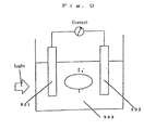
- this wet solar cell includes one electrode 901 formed of titania (titanium dioxide), which is a semiconductor, and another electrode 902 formed of platinum, ITO or the like, and these electrodes are held in an electrolyte solution 903, such as an iodine solution.
- the reaction principle of this wet solar cell is as follows.
- the titania which is a semiconductor
- the iodine ions which have been oxidized, receive the electrons again to be reduced at the counter electrode.
- the iodine ions are cyclically moved between both of the electrodes, thereby realizing the battery.
- this dye-sensitized solar cell is a wet cell employing an electrolyte, such as an iodine solution or the like, it is necessary to seal its solar cell containing the iodine solution as the electrolyte with a sealing material. Due to this structure, the dye-sensitized solar cell is subject to many problems in that, for example, leakage of electrolyte solution is liable to occur when the sealing is broken and the like.
- the dye-sensitized solar cell cannot have a practical life as a solar cell.
- the present invention is directed to a solar cell employing a titanium dioxide semiconductor, which includes a pair of electrodes; and a titanium dioxide semiconductor which is held between the electrodes, the surface and inside of the titanium dioxide semiconductor being formed with pores, and the titanium dioxide semiconductor being arranged so as to form a rectification barrier with respect to at least one of the electrodes.
- the rectification barrier is formed by contacting the titanium dioxide semiconductor with at least one of the electrodes, and the rectification barrier has a diode characteristic. According to this structure, it is possible to enhance the efficiency of power generation of the solar cell.
- the rectification barrier is the shottky barrier being formed by contacting the titanium dioxide semiconductor with at least one of said electrodes. According to this structure, it is also possible to enhance the efficiency of power generation of the solar cell.
- the rectification barrier is the PN junction being formed by contacting the titanium dioxide semiconductor with at least one of said electrodes. This also enables enhancement of the efficiency of power generation of the solar cell.
- the electrode, with which said titanium dioxide semiconductor forms the rectification barrier is formed in such a way as to penetrate into the surface of the titanium dioxide semiconductor and the inside thereof. This makes it possible to further increase the area (surface area) where the rectification barrier is formed, thereby further enhancing the efficiency of power generation of the solar cell.
- the titanium dioxide semiconductor has a porosity of 5 to 90%. This increases the contacting area between the titanium dioxide semiconductor and light (that is, the irradiated area by light), thereby enhancing the efficiency of power generation of the solar cell.
- the titanium dioxide semiconductor has a porosity of 15 to 50%. This further increases the contacting area between the titanium dioxide semiconductor and light (that is, the irradiated area by light), thereby further enhancing the efficiency of power generation of the solar cell.
- said titanium dioxide semiconductor has a porosity of 20 to 40%. This further more increases the contacting area between the titanium dioxide semiconductor and light (that is, the irradiated area by light), thereby furthermore enhancing the efficiency of power generation of the solar cell.
- the titanium dioxide semiconductor is porous and has the fractal structure. This also enhances the efficiency of power generation of the solar cell.
- the electrode with which said titanium dioxide semiconductor form the rectification barrier is formed from a transparent electrode made of ITO or the like, or a metallic electrode made of a metal selected from the group consisting of Al, Ni, Cr, Pt, Ag, Au, Cu, Mo, Ti, and Ta, or a metal compound containing therein any one or more of these metals. This also enhances the efficiency of power generation of the solar cell.
- the electrode with which said titanium dioxide semiconductor forms the rectification barrier includes a solid iodide. This also enhances the efficiency of power generation of the solar cell.
- said titanium dioxide semiconductor forms the rectification barrier includes CuI (copper iodide). This enhances the efficiency of power generation of the solar cell.
- said titanium dioxide semiconductor forms the rectification barrier includes AgI (silver iodide). This also enhances the efficiency of power generation of the solar cell.
- the electrodes are formed by vacuum evaporation. This makes it possible to reliably contact the titanium dioxide semiconductor with the electrode so that the efficiency of power generation of the solar cell is further enhanced.
- the electrode using use spattering method. This also makes it possible to reliably contact the titanium dioxide semiconductor with the electrode so that the efficiency of power generation of the solar cell is further enhanced.
- the electrode using use printing method. This also makes it possible to reliably contact the titanium dioxide semiconductor with the electrode so that the efficiency of power generation of the solar cell is further enhanced.
- the titanium dioxide semiconductor is subjected to visual rays absorbable processing for making it possible to absorb visible rays. This makes it possible for the titanium dioxide semiconductor to utilize light in the visual ray region, thereby enabling to enhancement of the efficiency of power generation of the solar cell.
- organic dye is adsorbed to said titanium dioxide semiconductor. This is a preferable means as the visual rays absorbable processing, which enables enhancement of the efficiency of power generation of the solar cell.
- inorganic dye is adsorbed to said titanium dioxide semiconductor. This is also preferable means as the visual rays absorbable processing, which also enables enhancement of the efficiency of power generation of the solar cell.
- the inorganic dye being adsorbed to said titanium dioxide semiconductor includes inorganic carbon. This is also a preferable method of performing the visual rays absorbable processing, thereby enabling enhancement of the efficiency of power generation of the solar cell.
- the inorganic dye being adsorbed to said titanium dioxide semiconductor includes an inorganic matter obtained by dying carbon. This is also a preferable method of performing the visual rays absorbable processing, thereby enabling enhancement of the efficiency of power generation of the solar cell.
- the titanium dioxide semiconductor has oxygen defects. This makes it possible for the titanium dioxide semiconductor to utilize light in the visual ray region, thereby enabling enhancement of the efficiency of power generation of the solar cell.
- the titanium dioxide semiconductor includes impurities such as Cr and/or V. This makes it possible to prevent the crystalline structure of the titanium dioxide semiconductor from being changed.
- Another aspect of the present invention is directed to a solar cell unit employing a titanium dioxide semiconductor, which includes a solar cell which includes a pair of electrodes, and a titanium dioxide semiconductor which is held between the electrodes, the titanium dioxide semiconductor being formed with pores, and first and second substrates which holds the solar cell therebetween.
- a solar cell unit which can utilize current and voltage of practically required levels, that is a solar cell unit which is excellent in power generation efficiency (photoelectric transfer efficiency).
- a solar cell unit has first and second substrates arranged so that solar rays enter from the side of one of the substrates, in which the other substrate arranged at the opposite side is coated with a reflection film or has a reflection film thereon.
- the first and second substrates are arranged so that solar rays enter from the side of one of the substrates, in which the other substrate arranged at the opposite side is coated with a reflection film or has a reflection film thereon.
- This arrangement makes it possible to prevent or suppress passing of the light effectively so that the solar cell unit can utilize the light more efficiently. With this result, it is possible to enhance the efficiency of power generation of the solar cell.
- the space between the first substrate and the second substrate is filled with an inert gas such as argon gas.
- an inert gas such as argon gas.
- At least one of the first and second substrates, arranged at the side from which solar rays enter, is formed into a transparent substrate or a translucent substrate formed of glass, plastic or synthetic resin. This arrangement makes it possible to reliably transmit the light to the light receiving surface of the solar cell cell.
- At least one of the first and second electrodes, arranged at the side from which solar rays enter has a top surface and a bottom surface, and an anti-reflection film is coated or placed on the tip surface or bottom surface.
- At least one of the first and second electrodes, arranged at the side from which solar rays enter has a top surface, and a light catalyst made of titanium dioxide (TiO 2 ) is coated on or placed on the top surface.
- a light catalyst made of titanium dioxide (TiO 2 ) is coated on or placed on the top surface.
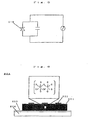
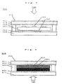
- Fig. 1 to Fig. 8 schematically show the structures, the circuit and the like of a solar cell and a solar cell units according to the present invention.
- the reference numerals 101, 201, 301, 401, 601, 701 and 801 used in Fig. 1 to Fig. 4 and Fig. 6 to Fig. 8 designate respectively a titanium dioxide semiconductor (titania semiconductor).
- titanium dioxide semiconductor titanium dioxide semiconductor
- the different reference numerals are assigned to designate the titania semiconductor in these drawings.
- corresponding elements or the same elements other than the titanium dioxide are also designated with different reference numerals.
- Fig. 1 is an illustration which schematically shows the structure of a solar cell (solar cell unit) 100, which is an embodiment of a solar cell employing a semiconductor according to the present invention.
- the solar cell 100 includes a first substrate 104, such as a glass substrate or a metal substrate, and a first electrode 103 formed on the first substrate 104.
- the first electrode 103 is formed from a transparent electrode made of ITO or the like or a metallic electrode (which is made of a metal selected from the group consisting of Al, Ni, Cr, Pt, Ag, Au, Cu, Mo, Ti and Ta, an alloy containing any one or more of these metals, or a compound containing any one of these metals).
- An anatase type titanium dioxide (TiO 2 ) semiconductor 101 is formed on the first electrode 103.
- the titanium dioxide (TiO 2 ) semiconductor is an n-type semiconductor.
- a comb-shaped (stripe-like) second electrode 102 is formed on the anatase type titanium dioxide (TiO 2 ) semiconductor 101.
- TiO 2 titanium dioxide
- the comb-shaped second electrode shown in Fig. 1 is illustrated to have three electrode teeth, a comb-shaped second electrode 102 of an actual model can have a more number of stripe-like comb-shaped electrode teeth.
- the second electrode 202 which is formed on the anatase type titanium dioxide (TiO 2 ) semiconductor 201, may be formed into a full-face type electrode which covers a part of or an entire of the surface of the titanium dioxide (TiO 2 ) semiconductor 201.
- a third electrode 205 that supports the second electrode may be formed on the second electrode 202.
- This third electrode includes a substrate, such as a glass substrate or a metallic substrate, and on the substrate there is formed a transparent electrode made of ITO or the like or a metallic electrode (which is made of a metal selected from the group consisting of Al, Ni, Cr, Pt, Ag, Au, Cu, Mo, Ti and Ta, or an alloy containing any one or more of these metals).
- each of the second electrodes 102, 202 shown in Fig. 1 and Fig. 2 is constructed from a metallic electrode (which is made of a metal selected from the group consisting of Al, Ni, Cr, Pt, Ag, Au, Cu, Mo, Ti and Ta, an alloy containing any one or more of these metals, a compound containing therein any one of the above-mentioned metals such as CuI, CuSCN, AgI, CuBr, Ag 2 S, RbAg 4 I 5 , AgBr, ⁇ -Al 2 O 3 (NaO ⁇ nAl 2 O 3 ), or the like).
- a metallic electrode which is made of a metal selected from the group consisting of Al, Ni, Cr, Pt, Ag, Au, Cu, Mo, Ti and Ta, an alloy containing any one or more of these metals, a compound containing therein any one of the above-mentioned metals such as CuI, CuSCN, AgI, CuBr, Ag 2 S, RbAg 4 I
- a rectification barrier (the Schottky barrier or the PN junction), which has an energy height corresponding to the difference in the work function between the titania semiconductor 101 or 201 and the first electrode or the second electrode, is formed in the interface therebetween, so that rectification occurs.
- the titanium dioxide (TiO 2 ) semiconductor when the titanium dioxide (TiO 2 ) semiconductor is in contact with the second electrode 102 or 202 and the work function of each of the second electrodes 102, 202 is larger than that of the titanium dioxide (TiO 2 ) semiconductor, rectification occurs due to the presence of the Schottky barrier or the PN junction.
- any one of the materials described above, in particular a material having the ion conduction property, is preferably employed.
- one kind of or two or more kinds of metal halide compounds such as a metal iodide compound such as CuI or AgI, and a metal bromide compound, such as AgBr, may be used, for example.
- metal iodide compounds such as CuI and AgI.
- Fig. 3 and Fig. 4 show the structure of the solar cell of the embodiment according to the present invention.
- Fig. 3 shows the situation in which an electrode 302 of the solar cell (corresponding to the second electrode 102, 202 of Fig. 1 and Fig. 2), which is made of a metal, a metal alloy, a metal compound or the like, is in contact with or joined to a titanium dioxide (TiO 2 ) semiconductor 301.
- an electrode 302 of the solar cell corresponding to the second electrode 102, 202 of Fig. 1 and Fig. 2
- TiO 2 titanium dioxide
- the second electrode 302 penetrates into the pores of the titanium dioxide semiconductor 301 so that the titanium dioxide semiconductor 301 and the second electrode 302 form therebetween the Schottky barrier or the PN junction. With this result, the surface area of the Schottky barrier or the PN junction, which is formed between the metal (the metallic electrode 302) and the semiconductor (the titanium dioxide (TiO 2 ) semiconductor 301), is increased.
- the titanium dioxide semiconductor 301 which is an n-type semiconductor
- an electrode of CuI the second electrode 302
- the PN junction is created therebetween, so that a diode is formed in the junction part due to the PN junction.
- Fig. 4 shows the situation in which solar rays strike the solar cell shown in Fig. 1. Specifically, solar rays strike the metallic electrode (represented by 402) and a part of the titanium dioxide (TiO 2 ) semiconductor (represented by 401) where no metallic electrode is formed.
- the metallic electrode represented by 402
- TiO 2 titanium dioxide
- Fig. 3 and Fig. 4 the arrows indicate the traveling directions of the rays, and these figures show the situation in which the rays strike on the surface and enter the pores of the titanium dioxide semiconductor.
- the titanium dioxide (TiO 2 ) semiconductor 401 and the metallic electrode (second electrode) 402 are in contact with each other to form therebetween the Schottky barrier or the PN junction.
- the metallic electrode 402 formed on the surface of the titanium dioxide (TiO 2 ) semiconductor penetrates into the pores of the titanium dioxide semiconductor 401.
- the surface area of the Schottky barrier or the PN junction, which is formed between the metal (the metallic electrode 402) and the semiconductor (the titanium dioxide (TiO 2 ) semiconductor 401) is increased.
- the titanium dioxide semiconductor 401 which is an n-type semiconductor
- the electrode of CuI the second electrode 402
- PN junction is created therebetween, so that a diode is formed in the junction part due to the PN junction.
- the metallic electrode 402 which is provided on the surface of the titanium dioxide (TiO 2 ) semiconductor, is constructed from a transparent electrode made of ITO or the like, or ametallic electrode (which is made of ametal selected from the group consisting of Al, Ni, Cr, Pt, Ag, Au, Cu, Mo, Ti and Ta, an alloy containing therein any one of these metallic materials, or a compound, containing therein the above-mentioned metal, such as CuI, CuSCN, AgI, Ag 2 S, RbAg 4 I 5 , CuBr, AgBr, ⁇ -Al 2 O 3 (NaO ⁇ nAl 2 O 3 ), or the like), and the metal electrode 402 is formed on the surface of the titanium dioxide (TiO 2 ) semiconductor by utilizing the vacuum evaporation method, the sputtering method or the printing method or the like.
- the material having the ion conduction property is preferably used for the constituent material of the metallic electrode 402.
- one kind of, or two or more kinds of, metal halide compounds such as a metal iodide compound such as CuI or AgI, and a metal bromide compound, such as AgBr, may be used, for example.
- metal iodide compounds such as CuI and AgI.
- the metallic electrode 402 which is formed on the surface of the titanium dioxide (TiO 2 ) semiconductor, is made of CuI (copper iodide), CuI is dissolved in a solvent, such as acetonitrile, to obtain a saturated solution, and then the saturated solution thus obtained is dropped onto the surface of the titanium dioxide semiconductor or on the third electrode 205 shown in Fig. 2, and then it is heated at a temperature of 100 to 180 degrees, thereby obtaining the metallic electrode 402.
- a solvent such as acetonitrile
- the titanium dioxide (TiO 2 ) semiconductor of the present invention has a very large porosity, solar rays not only strike on the surface of the titanium dioxide (TiO 2 ) semiconductor, but also enter the pores of the titanium dioxide (TiO 2 ) semiconductor, and thus rays that enter cause multiple-reflection repeatedly within the pores, as indicated by the arrows in Fig. 3 and Fig. 4, to cause the photovoltaic effect in the titanium dioxide (TiO 2 ) semiconductor.
- the contact part between the metal and the semiconductor that is, the Schottky barrier part or the PN junction part
- the contact part between the metal and the semiconductor that is, the Schottky barrier part or the PN junction part
- the contact part between the metal and the semiconductor that is, the Schottky barrier part or the PN junction part
- the contact part between the metal and the semiconductor that is, the Schottky barrier part or the PN junction part
- the contact part between the metal and the semiconductor that is, the Schottky barrier part or the PN junction part
- the rays which have entered the pores of the titanium dioxide semiconductor are reflected repeatedly in the pores and a part of the rays pass through downwardly.
- these rays are reflected by the surface of the flat lower electrode (first electrode) 103 shown in Fig. 1, or by a reflecting plate 714 shown in Fig. 7 (which will be described later) or a reflecting plate 816 shown in Fig. 8 (which will be described later), and they reenter the surface of the titanium dioxide semiconductor that is the pores thereof again, thereby causing the photoelectromotive force.
- Each of the titania semiconductors 301, 401 is the oxide semiconductor made of an anatase type titanium dioxide, which is formed by sintering fine powder of titanium (Ti) having the particle size of about 10 nm to about 100 ⁇ m, and then oxidizing it, or the oxide semiconductor which is formed by sintering fine powder of an anatase type titania (TiO 2 ) having the particle size of about 5 nm to about 2,000 nm.
- Ti titanium oxide semiconductor made of an anatase type titanium dioxide, which is formed by sintering fine powder of titanium (Ti) having the particle size of about 10 nm to about 100 ⁇ m, and then oxidizing it, or the oxide semiconductor which is formed by sintering fine powder of an anatase type titania (TiO 2 ) having the particle size of about 5 nm to about 2,000 nm.
- Each of the titanium dioxide semiconductors 301, 401 has a very high porosity (void ratio), that is porous, thus it has the so-called fractal structure.
- the porous titanium dioxide semiconductor 301 or 401 is formed from an anatase type titania semiconductor having the porosity (void ratio) of 5 to 90 %.
- the titanium dioxide semiconductor 301 or 401 is formed from an anatase type titania semiconductor having the porosity (void ratio) of 15 to 50 %, and more preferably, it is formed from an anatase type titania semiconductor having the porosity of 20 to 40 %.
- the surface area of the titania electrode is remarkably increased as compared with the case where the titania electrode is formed into a flat-shaped plate.
- a portion of the titania defined by 1 cm 2 in a plane can have a total surface area of 1,000 to 10,000 cm 2 .
- the contact area between the titania and solar rays is also increased, the amount of the current flowing therethrough is mathematically expected to be 1,000 to 10,000 times as large as the case where the titania electrode is formed into a flat-shaped plate.
- the titania semiconductor of the present invention is subjected to the processing for sensitizing to absorption wavelength of rays, such as solar rays, so as to be able to react with the rays up to the visible ray region.
- examples of such processing include (1) a method in which dye is adsorbed on the porous surface of the titania semiconductor (the dye adsorption method), (2) a method in which oxygen defects are formed in the titania to reduce the band gap in order to sensitize to the visible rays (the oxygen defect method), and (3) a method in which the titania is doped with a very small quantity of impurities (the impurity doping method), and so forth, and one kind of, or two or more kinds of, these methods can be used alone or in combination with other method.
- the dye adsorption method the dye adsorption method
- the oxygen defect method a method in which oxygen defects are formed in the titania to reduce the band gap in order to sensitize to the visible rays
- the impurity doping method the impurity doping method
- the first method (the dye adsorption method) will hereinbelow be described in detail.
- Each of the titania semiconductors 301, 401 shown in Fig. 3 and Fig. 4 is the oxide semiconductor made of an anatase type titanium dioxide, which is formed by sintering fine powder of titanium (Ti) having the particle size of about 10 nm to about 100 ⁇ m, and then oxidizing it, or the oxide semiconductor which is formed by sintering fine powder of an anatase type titania (TiO 2 ) having the particle size of about 5 nm to about 2,000 nm.
- Each of the titanium dioxide semiconductors 301, 401 has a very high porosity, that is porous. Thus it has what is referred to as a fractal structure.
- the porous titanium dioxide semiconductor 301 or 401 is formed of an anatase type titania semiconductor having the porosity (void ratio) of 5 to 90 %.
- the titanium dioxide semiconductor 301 or 401 is formed of an anatase type titania semiconductor having the porosity (void ratio) of 15 to 50 %, and more preferably, it is formed of an anatase type titania semiconductor having the porosity of 20 to 40 %.
- dye is, in advance, adsorbed on the surface of the titanium dioxide semiconductor and inside the pores thereof.
- organic dye metal organic dye such as ruthenium complex
- inorganic dye carbon black containing therein inorganic carbon and the like
- the dye is previously dissolved in a solvent, such as alcohol, and the titanium dioxide semiconductor 301 or 401 is dipped in this solution, so that the dye is adsorbed on the surface of the titanium dioxide semiconductor 301 or 401 and inside the pores thereof. Thereafter, the titanium dioxide semiconductor 301 or 401, which is pulled up from the solution, and then it is dried naturally, whereby the dye is adsorbed and fixed on the surface of the titanium dioxide semiconductor 301 or 401 and inside the pores thereof. In this case, in order to make the dye adsorbed more firmly, it is effective to dry the titanium dioxide semiconductor 301 or 401 with a clean oven or the like at a temperature of about 60 to 100 degrees.
- a solvent such as alcohol
- the mean particle size of the titanium dioxide powder is not particularly limited, but it is preferably in the range of about 5 nm to about 10 ⁇ m, and it is more preferably in the range of about 5 nm to about 100 nm, for example.
- the titanium dioxide (TiO 2 ) powder is subjected to reduction processing at a temperature of 600 to 1,000 degrees to reduce the oxygen contained in the titanium dioxide (TiO 2 ) so that the titanium dioxide semiconductor having oxygen defects is formed.
- the property of the titanium dioxide semiconductor at this time is of an n-type.
- the crystal structure of the anatase type titanium dioxide (TiO 2 ) begins to change into that of the rutile type. Therefore, the titanium dioxide (TiO 2 ) having oxygen defects can be formed into three states including the state in which only the anatase type titanium dioxide is present, the state in which the anatase type titanium dioxide and the rutile type titanium dioxide are mixedly present, and the state in which only the rutile type titanium dioxide is present.
- the reduction processing which is employed at this stage is carried out in a hydrogen atmosphere.
- the reduction of the oxygen contained in the titanium dioxide (TiO 2 ) is promoted by hydrogen, so that the temperature of the reduction processing can be set to a lower level. Therefore, it is also possible to subject the anatase type titanium dioxide (TiO 2 ) to the reduction processing as it is.
- Fig. 6 shows the structure of the titania semiconductor of the embodiment according to the present invention.
- the titania contains therein a very small quantity of impurities, such as Cr (chromium) andV (vanadium), in the range of 0.1 to 2.5 ⁇ mol/g, and also more ideally, it is preferable that the titania contains therein impurities, such as Cr and V, in the range of 1.5 to 2.0 ⁇ mol/g.
- impurities such as Cr (chromium) andV (vanadium
- the titania semiconductor of the present invention since the titania semiconductor of the present invention is subjected to the processing for sensitizing to the absorption wavelength of rays, such as solar rays, so as to be able to react with the rays up to the visible ray region, it can absorb the visible rays having the wavelength of equal to or longer than 400 nm (normally, this means the rays having the wavelength of 400 to 750 nm) which cannot be efficiently absorbed by the normal titania semiconductor. Therefore, the titania semiconductor of the present invention can absorb solar rays at the practical level. As a result, the efficiency of the solar cell can be greatly enhanced.
- the titania semiconductor employed in the present invention is formed by utilizing what is referred to as Powder Injection Molding method (in general, it is called the PIM Method), or what is referred to as Metal Injection Molding Method (in general, it is called the MIM method).
- Powder Injection Molding method in general, it is called the PIM Method
- MIM method Metal Injection Molding Method
- a resin binder of 99 to 50 % in the volume ratio is added to titanium fine powder, having the particle size of about 20 to 2,000 nm, and then they are kneaded to form a source compound, having the low viscosity (in the range of 1,000 to 3,000 P) with which the injection molding can be carried out.
- Cr or V is added thereto in order to increase the absorption wavelength width of rays.
- This may be added to the source compound, either in the state of the oxide of Cr (CrO 3 ), or in the state of the oxide of V, or added to the source compound in the state of pure Cr or in the state of pure V.
- the debound titanium fine powder (brown body) is sintered together with the above-mentioned additive.
- the titanium fine powder is oxidized through this sintering process to become the anatase type titania (titanium dioxide).
- the rutile type titania is thermally stable and the crystal structure of the anatase type titania is changed into the rutile type titania through heating at the temperature of equal to or higher than 900 degrees, the debinding process and the sintering process, including the oxidation, must be carried out at the temperature of equal to or lower than 900 degrees so that the crystal structure of the titanium oxide can be kept as the anatase type titanium dioxide.
- MoO 3 mobdenum oxide
- this sintering assistant is not limited to MoO 3 (molybdenum oxide), and hence any of other sintering assistants can be utilized as long as its melting point is equal to or lower than 900 degrees.
- the following method in which after titanium fine powder has been sintered in a vacuum atmosphere at the temperature of about 1,200 degrees once, the resultant sintering body is resintered in an oxygen atmosphere at the temperature of equal to or lower than 900 degrees to oxidize the titanium sintered body, thereby obtaining a titanium dioxide semiconductor.
- the titania semiconductor may be formed into a film (a thick film or a thin film) by utilizing various kinds of coating or spraying methods and apparatuses, such as dipping, doctor blade, spin coating, brush application, spray coating, and roll coater.
- a titania semiconductor having a desired pattern shape can be readily obtained by employing a masking, for example.
- the mean particle size of the titanium oxide powder is not particularly limited, but, for example, it is preferably in the range of about 5 nm to 10 ⁇ m, and is more preferably in the range of about 5 to 100 nm.
- Use of the titanium dioxide powder having the mean particle size within the above-mentioned range makes it possible to enhance the uniformity of the titanium oxide powder in the coating liquid (semiconductor material), as will be described later in detail.
- the titanium oxide powder having the small mean particle size as described above it becomes possible to obtain a super porous titania semiconductor, which makes it possible for the light receiving surface of the titania semiconductor to have an increased contact area with rays.
- the amount of dye adsorbed to the titania semiconductor can be greatly increased.
- the fine particle titanium oxide powder having the particle size of about 5 to 100 nm, is suspended into a suitable amount of water (e.g., distilled water, super-pure water, ion exchange water, RO water or the like).
- a suitable amount of water e.g., distilled water, super-pure water, ion exchange water, RO water or the like.
- a stabilizing agent such as nitric acid or the like, is added to such suspension, and then they are sufficiently kneaded in a mortar made of agate (or made of alumina).
- the above-mentioned water is added to such suspension to be further kneaded therewith.
- the mixing ratio between the above-mentioned stabilizing agent and the water should preferably be in the range of 10:90 to 40:60 in the volume ratio, and more preferably in the range of 15:85 to 30:70.
- the viscosity of such suspension should be in the range of about 0.2 to about 30 cps, for example.
- the coating liquid (semiconductor material) is prepared.
- the surfactant may be any one of the surfactants including a cationic surfactant, an anionic surfactant, a bi-ionic surfactant, and a non-ionic surfactant. However, it is preferable to use the non-ionic surfactant.
- a surface modification reagent for the titanium oxide such as acetic acid or acetylacetone, may also be employed.
- additives such as a binder e.g. polyethlene glycol (PEG), a plasticizer, and an antioxidant, may be added to the coating liquid (semiconductor material).
- additives such as the binder e.g. polyethlene glycol (PEG), the plasticizer and the antioxidant, a is effective for increasing the viscosity of the suspension to provide a coating liquid (semiconductor material) in paste form.
- the PEG serves to increase the viscosity of the titania paste and also acts as a binder for the fine particle titania when sintering the titania semiconductor.
- the PEG contributes to increasing the porosity of the titania semiconductor because the component of the PEG which is unnecessary as the binder is volatilized during the sintering process.
- the coating liquid as described above is applied to the upper surface of the first electrodes 103, 203 shown in Fig. 1 or Fig. 2 by the coating method (e.g., the dipping or the like), and it is then dried to form a film made of the semiconductor material.
- the operation of the application and the drying of the coating liquid may also be carried out plural times to obtain a laminate of films of the semiconductor material.
- the film, made of the semiconductor material is subjected to a heat treatment (e.g., the sintering or the like) at the temperature of about 250 to 500 degrees for about 0.5 to 3 hours to obtain the titanium semiconductor 101, 201.
- a heat treatment e.g., the sintering or the like
- the temperature of about 250 to 500 degrees for about 0.5 to 3 hours to obtain the titanium semiconductor 101, 201.
- Fig. 7 shows an example of the structure of a solar cell unit as a module (unit) of the solar cell of the present invention.
- a semiconductor made of titanium dioxide (a titanium dioxide semiconductor, that is a titania semiconductor) 701 is held between one pair of electrodes including an upper electrode (second electrode) 702 and a lower electrode (first electrode) 703.
- Each of these electrodes 702 and 703 is formed of a transparent electrode, such as ITO or a metallic electrode (which is made of a metal which is selected from the group consisting of Al, Ni, Cr, Pt, Ag, Au, Cu, Mo, Ti and Ta, an alloy containing any one or more of these metals, or a compound containing therein any one or more of the above-mentioned metals, such as CuI, CuSCN, AgI, Ag 2 S, RbAg 4 I 5 , AgBr or ⁇ -Al 2 O 3 (NaO ⁇ nAl 2 O 3 ) or the like).
- the upper electrode 702 may be either a stripe-like comb-shaped electrode including a plurality of electrode theeth, as shown in Fig. 1, or a full-face electrode, as shown in Fig. 2.
- the lower electrode 703 may be either a flat electrode, which is in contact with the titanium dioxide semiconductor 701, as shown in Fig. 1, or a stripe-like comb-shaped electrode, an electrode which is not a flat electrode.
- the direction of solar rays entering this solar cell cell (the solar cell unit) 700 is arbitrarily determined depending on the shape and the film quality of the electrode (s) such that the rays, such as solar rays, strike on the titanium dioxide semiconductor 701. Note that, in the solar cell unit 700 of this example, the unit is used so that the rays are made to enter from the upper side in Fig. 7.
- the space between the substrates 711 and 715 may also be filled with an inert gas, such as argon gas.
- a reflecting film (reflecting plate) 714 is formed on the upper surface of the lower substrate 715. As a result, the rays, which have passed through the titanium dioxide semiconductor 701, can be reflected towards the titanium dioxide semiconductor 701 again. However, it is to be noted that this reflecting film 714 may be omitted if it is unnecessary.
- an antireflection film 712 is applied to (provided on) the lower surface of the upper substrate 711.
- the uppermost surface of the upper substrate 711 is coated (arranged) with a thin film 716 made of titanium dioxide (TiO 2 ) having photocatalyst function, since the solar cell unit 700 of the present invention is normally placed out-doors to generate electricity.
- a thin film 716 made of titanium dioxide (TiO 2 ) provided on the upper substrate (cover glass) 711 of the solar cell unit 700 of the present invention, the cover glass 711 of the solar cell unit 700 can be prevented from becoming dirty and being contaminated due to carbon dioxide exhausted from automobiles and the like and organic contaminants.
- Fig. 8 shows another example of the structure of a solar cell unit as a module (unit) of the solar cell of the present invention.
- the solar cell unit 800 shown in Fig. 8 includes a lower substrate 815, a lower electrode (first electrode) 803, a titanium dioxide semiconductor 801, an upper electrode (second electrode) 802, a third electrode 812, and an upper substrate 811. Each of these elements is formed into a plate-like shape, and they are laminated in this order.
- Each of the lower substrate 815, the lower electrode 803, the titanium dioxide semiconductor 801, the upper electrode 802, the third electrode 812 and the upper substrate 811 is formed into a plate-shape or a layer-shape.
- a sealing material 813 is provided between the lower electrode 803 and the third electrode 812, and the side face of the solar cell unit is hermetically sealed therewith.
- both of the titanium dioxide semiconductor 801 and the upper electrode 802 are accommodated in the space defined by the sealing material 813, the lower electrode 803 and the third electrode 812.
- this space may be filled with an inert gas, such as argon gas (Ar).
- the titanium dioxide semiconductor 801 may have the same structure as that of each of the above-mentioned titanium dioxide semiconductors 101, 201, 301, 401, 601 and 701.
- the upper substrate 811 and the lower substrate 815 may have the same structures as those of the upper substrate 711 and the lower substrate 715 as described above, respectively.
- the upper electrode 802 and the lower electrode 803 may have the same structures as those of the upper electrode 702 and the lower electrode 703 as described above, respectively.
- the third electrode 812 may be constructed from a transparent electrode made of ITO or the like or a metallic electrode (which is made of metal which is selected from the group consisting of Al, Ni, Cr, Pt, Ag, Au, Cu, Mo, Ti and Ta, an alloy containing therein any one or more of these metallic materials, or the like).
- sealing material 813 may have the same structure as that of the above-mentioned sealing material 713.
- the solar cell unit 800 of this embodiment is used so that rays are made to enter from the lower side in Fig. 8.
- a reflecting film (reflecting plate) 816 is provided on the upper surface of the upper substrate 811, so that the rays which have passed through the titanium dioxide semiconductor 801 can be reflected towards the titanium dioxide semiconductor 801 again.
- an antireflection film having the same structure as that of the above-mentioned antireflection film 712, may be provided on the lower surface of the lower substrate 815.
- a thin film having the same structure as that of the above-mentioned thin film 716 may be provided on the lower surface of the lower substrate 815.
- Satisfying such a condition means that the titanium dioxide semiconductor 101 is low in directivity to the light, that is, it has the isotropy. Therefore, the solar cells and solar cell units 100, each having such a titanium dioxide semiconductor 101, can generate electricity with higher efficiency almost over the entire duration of hours of sunlight of the sun.
- the solar cell and the solar cell unit of the present invention have been described with reference to Fig. 1 to Fig. 8.
- the present invention is not intended to be limited thereto.
- the elements or components constituting the solar cell and the solar cell unit may be replaced with those having other structures capable of performing the same functions.
- the solar cell and the solar cell unit of the present invention may be those which are obtained by combining arbitrary two or more structures of Fig. 1 to Fig. 8.
- a solar cell employing a titanium dioxide (TiO 2 ) electrode has the porosity of 5 to 90 %, that is the porosity is very high, and hence the surface area of the titania is remarkably increased as compared with the conventional wet solar cell in which a titania electrode is formed into a flat-shaped plate.
- TiO 2 titanium dioxide
- a portion of the titania defined by 1 cm 2 in a plane can have a total surface area of 1,000 to 10,000 cm 2 .
- the amount of the current flowing therethrough is mathematically expected to be 1,000 to 10,000 times as large as the case where the titania electrode is formed into a flat-shaped plate.
- the titanium dioxide semiconductor contains therein impurities, such as Cr (chromium) and V (vanadium) in the range of 0.1 to 2.5 ⁇ mol/g, it becomes possible to absorb the visible rays having the wavelength of equal to or longer than 400 nm (normally, this means the rays having the wavelength of 400 to 750 nm) which cannot be efficiently absorbed by the normal titania semiconductor, so that the efficiency of the solar cell can be greatly enhanced.
- impurities such as Cr (chromium) and V (vanadium) in the range of 0.1 to 2.5 ⁇ mol/g
Landscapes
- Engineering & Computer Science (AREA)
- Power Engineering (AREA)
- Microelectronics & Electronic Packaging (AREA)
- Chemical & Material Sciences (AREA)
- Chemical Kinetics & Catalysis (AREA)
- Electrochemistry (AREA)
- Inorganic Chemistry (AREA)
- Physics & Mathematics (AREA)
- Electromagnetism (AREA)
- Hybrid Cells (AREA)
- Photovoltaic Devices (AREA)
Abstract
Description
Claims (30)
- A solar cell employing a titanium dioxide semiconductor, comprising:a pair of electrodes; anda titanium dioxide semiconductor which is disposed between the electrodes, the surface and interior of the titanium dioxide semiconductor being formed with pores, and the titanium dioxide semiconductor being arranged so as to form a rectification barrier with respect to at least one of the pair of electrodes.
- The solar cell as set forth in claim 1, wherein said rectification barrier is formed by contacting the titanium dioxide semiconductor with at least one of said pair of electrodes, and the rectification barrier has a diode characteristic.
- The solar cell as set forth in claim 1 or 2, wherein the rectification barrier is the shottky barrier being formed by contacting the titanium dioxide semiconductor with at least one of said pair of electrodes.
- The solar cell as set forth in claim 1 or 2, wherein the rectification barrier is the PN junction being formed by contacting the titanium dioxide semiconductor with at least one of said pair of electrodes.
- The solar cell as set forth in any one of claims 1 to 4, wherein the electrode, with which said titanium dioxide semiconductor forms the rectification barrier, is formed in such a way as to penetrate into the surface of the titanium dioxide semiconductor and the interior thereof.
- The solar cell as set forth in any one of claims 1 to 5, wherein said titanium dioxide semiconductor has a porosity of 5 to 90%.
- The solar cell as set forth in any one of claims 1 to 5, wherein said titanium dioxide semiconductor has a porosity of 15 to 50%.
- The solar cell as set forth in any one of claims 1 to 5, wherein said titanium dioxide semiconductor has a porosity of 20 to 40%.
- The solar cell as set forth in any one of claims 1 to 8, wherein said titanium dioxide semiconductor is porous and has the fractal structure.
- The solar cell as set forth in any one of claims 1 to 9, wherein the electrode with which said titanium dioxide semiconductor form the rectification barrier is formed from a transparent electrode made of ITO or the like, or a metallic electrode made of a metal selected from the group consisting of Al, Ni, Cr, Pt, Ag, Au, Cu, Mo, Ti, and Ta, or a metal compound containing therein any one or more of these metals.
- The solar cell as set forth in any one of claims 1 to 9, wherein the electrode with which said titanium dioxide semiconductor forms the rectification barrier includes a solid iodide.
- The solar cell as set forth in claim 11, wherein the electrode with which said titanium dioxide semiconductor forms the rectification barrier includes CuI (copper iodide).
- The solar cell as set forth in claim 11, wherein the electrode with which said titanium dioxide semiconductor forms the rectification barrier includes AgI (silver iodide).
- The solar cell as set forth in any one of claims 1 to 13, wherein the electrodes are formed by vacuum evaporation.
- The solar cell as set forth in any one of claims 1 to 13, wherein the electrodes are formed by spattering.
- The solar cell as set forth in any one of claims 1 to 13, wherein the electrodes are formed by printing.
- The solar cell as set forth in any one of claims 1 to 16, wherein said titanium dioxide semiconductor is subjected to visual rays absorbable processing to enable absorption of visible rays.
- The solar cell as set forth in claim 17, wherein organic dye is adsorbed to said titanium dioxide semiconductor.
- The solar cell as set forth in claim 17, wherein inorganic dye is adsorbed to said titanium dioxide semiconductor.
- The solar cell as set forth in claim 19, wherein the inorganic dye, being adsorbed to said titanium dioxide semiconductor, includes inorganic carbon.
- The solar cell as set forth in claim 19, wherein the inorganic dye, being adsorbed to said titanium dioxide semiconductor, includes an inorganic matter obtained by dying carbon.
- The solar cell as set forth in claim 17, wherein said titanium dioxide semiconductor has oxygen defects.
- The solar cell as set forth in claim 17, wherein said titanium dioxide semiconductor includes impurities such as Cr and/or V.
- The solar cell as se t forth in claim 23, wherein said titanium dioxide semiconductor includes Mo.
- A solar cell unit employing a titanium dioxide semiconductor, comprising:a solar cell which includes a pair of electrodes, and a titanium dioxide semiconductor disposed between the electrodes, the titanium dioxide semiconductor being formed with pores, andfirst and second substrates which holds the solar cell therebetween.
- The solar cell unit as set forth in claim 25, wherein the first and second substrates are arranged so that solar rays enter from the side of one of the substrates, in which the other substrate being arranged at the opposite side is coated with a reflection film or having a reflection film thereon.
- The solar cell unit as set forth in claim 25 or 26, wherein the space between the first substrate and the second substrate is filled with an inert gas such as argon gas.
- The solar cell unit as set forth in any one of claims 25 to 27, wherein at least one of the first and second substrates being arranged at a side from which solar rays enter is formed into a transparent substrate or a translucent substrate formed of glass, plastic or synthetic resin.
- The solar cell unit as set forth in any one of claims 25 to 28 wherein at least one of the first and second substrates arranged at a side from which solar rays enter has a top surface and a bottom surface, and an anti-reflection film is coated or placed on the top surface or bottom surface.
- The solar cell unit as set forth in any one of claims 25 to 29 wherein at least one of the first and second substrates arranged at the side from which solar rays enter has a top surface, and a light catalyst made of titanium dioxide (TiO2) is coated on or placed on the top surface of the substrate.
Applications Claiming Priority (5)
| Application Number | Priority Date | Filing Date | Title |
|---|---|---|---|
| JP37120799 | 1999-12-27 | ||
| JP37120799 | 1999-12-27 | ||
| JP2000342007 | 2000-11-09 | ||
| JP2000342007 | 2000-11-09 | ||
| PCT/JP2000/009241 WO2001048833A1 (en) | 1999-12-27 | 2000-12-26 | Solar cell and solar cell unit |
Publications (2)
| Publication Number | Publication Date |
|---|---|
| EP1178542A1 true EP1178542A1 (en) | 2002-02-06 |
| EP1178542A4 EP1178542A4 (en) | 2006-03-08 |
Family
ID=26582298
Family Applications (1)
| Application Number | Title | Priority Date | Filing Date |
|---|---|---|---|
| EP00987742A Withdrawn EP1178542A4 (en) | 1999-12-27 | 2000-12-26 | SOLAR CELL AND SOLAR CELL UNIT |
Country Status (8)
| Country | Link |
|---|---|
| US (2) | US6683361B2 (en) |
| EP (1) | EP1178542A4 (en) |
| JP (1) | JP4613468B2 (en) |
| KR (1) | KR100492039B1 (en) |
| CN (1) | CN1181563C (en) |
| AU (1) | AU777191B2 (en) |
| TW (1) | TW563259B (en) |
| WO (1) | WO2001048833A1 (en) |
Cited By (3)
| Publication number | Priority date | Publication date | Assignee | Title |
|---|---|---|---|---|
| EP1489628A4 (en) * | 2002-03-26 | 2008-01-02 | Fujikura Ltd | Conductive glass and photoelectric conversion device using same |
| EP1437790A4 (en) * | 2002-06-14 | 2010-05-12 | Panasonic Elec Works Co Ltd | PHOTOELECTRIC TRANSDUCER AND METHOD OF MANUFACTURING THE SAME |
| CN103515107A (en) * | 2013-10-21 | 2014-01-15 | 河南科技大学 | Double-network overlapped dye-sensitized solar cell |
Families Citing this family (36)
| Publication number | Priority date | Publication date | Assignee | Title |
|---|---|---|---|---|
| KR100416502B1 (en) * | 2001-10-18 | 2004-01-31 | 한국전자통신연구원 | Dye-sensitized solar cells including titanium silicalite-2 |
| JP2003303629A (en) | 2002-04-11 | 2003-10-24 | Sony Corp | Dye-sensitized solar cells |
| KR100499271B1 (en) * | 2002-09-09 | 2005-07-01 | 한국전자통신연구원 | Flexible dye-sensitized solar cells and method for manufacturing the same |
| WO2004030139A1 (en) * | 2002-09-25 | 2004-04-08 | Sharp Corporation | Dye-sensitized solar cell |
| US7290093B2 (en) * | 2003-01-07 | 2007-10-30 | Intel Corporation | Cache memory to support a processor's power mode of operation |
| US20090028740A1 (en) * | 2003-04-14 | 2009-01-29 | S'tile | Method for the production of semiconductor granules |
| AU2003902117A0 (en) * | 2003-05-05 | 2003-05-22 | Sustainable Technologies International Pty Ltd | Photovoltaic device |
| CN100438206C (en) * | 2003-07-14 | 2008-11-26 | 株式会社藤仓 | Electrolyte composition, photoelectric conversion element using same, and dye-sensitized solar cell |
| JP2005064493A (en) * | 2003-07-31 | 2005-03-10 | Kyocera Corp | Photoelectric conversion device and photovoltaic device using the same |
| CN100358161C (en) * | 2003-11-01 | 2007-12-26 | 鸿富锦精密工业(深圳)有限公司 | Dye sensitized solar cell and its battery |
| KR100572852B1 (en) * | 2003-12-24 | 2006-04-24 | 한국전자통신연구원 | Bendable solar cell and its manufacturing method |
| KR101030040B1 (en) * | 2004-02-19 | 2011-04-20 | 삼성에스디아이 주식회사 | Dye-Sensitized Solar Cell Comprising Porous Membrane and Manufacturing Method Thereof |
| JP4792711B2 (en) * | 2004-06-01 | 2011-10-12 | 凸版印刷株式会社 | Dye-sensitized solar cell |
| DE102004037478A1 (en) * | 2004-07-30 | 2006-08-10 | Nonnenbruch, Fritz | New solid/liquid material, with specific spectral bands in e.g. resonance Raman-spectrum, elements and stability, useful in electronics and photochemistry comprises polyoxometallate of molybdenum, tungsten and vanadium |
| DE102004054757B4 (en) * | 2004-11-12 | 2007-07-05 | Fraunhofer-Gesellschaft zur Förderung der angewandten Forschung e.V. | Process for producing the photoelectrode of a solar cell |
| JP4972921B2 (en) * | 2005-01-14 | 2012-07-11 | セイコーエプソン株式会社 | Method for manufacturing photoelectric conversion element |
| CN100413094C (en) * | 2005-08-09 | 2008-08-20 | 中国科学院物理研究所 | A kind of electrolyte and its application based on aluminum iodide |
| US20070056627A1 (en) * | 2005-09-09 | 2007-03-15 | Atomic Energy Council - Institute Of Nuclear Energy Research | Sensitized semiconductor solar cell |
| JP5105764B2 (en) * | 2006-04-20 | 2012-12-26 | ラピスセミコンダクタ株式会社 | Dye-sensitized solar cell |
| KR100810730B1 (en) * | 2006-06-19 | 2008-03-07 | (주)인솔라텍 | Manufacturing Method of Light Absorption Layer for Solar Cell |
| DE102006028429B3 (en) * | 2006-06-21 | 2007-06-28 | Fachhochschule Kiel | Coating production method for producing a solar absorber coating coats a substrate with a titanium precursor solution so as to generate a layer of titanium dioxide according to a sol-gel technique |
| TWI306314B (en) * | 2006-09-27 | 2009-02-11 | Ind Tech Res Inst | Method of sealing solar cells |
| KR100828262B1 (en) * | 2006-10-27 | 2008-05-07 | 미리넷솔라 주식회사 | Manufacturing process of solar cell module for solar power generation |
| TW200919728A (en) * | 2007-10-19 | 2009-05-01 | Iner Aec Executive Yuan | Multi-layer thin film electrode structure and method of forming same |
| KR100928941B1 (en) * | 2007-11-07 | 2009-11-30 | 한국과학기술연구원 | Dye-Sensitized Solar Cell and Manufacturing Method Thereof |
| JP4900443B2 (en) * | 2009-09-30 | 2012-03-21 | 大日本印刷株式会社 | Dye-sensitized solar cell |
| KR20110123102A (en) * | 2010-05-06 | 2011-11-14 | 한국전자통신연구원 | Dye-Sensitized Solar Cell Applying Polymer Film with Mirror Reflection |
| KR101097679B1 (en) * | 2010-05-25 | 2011-12-23 | 삼성전기주식회사 | Device for converting energy and method for manufacturing the device, and electronic apparatus with the device |
| JP2013016358A (en) * | 2011-07-04 | 2013-01-24 | Sony Corp | Photoelectric conversion element module |
| JP2013026030A (en) * | 2011-07-21 | 2013-02-04 | Sony Corp | Photoelectric conversion module and building |
| TWI467784B (en) * | 2011-12-21 | 2015-01-01 | Univ Nat Cheng Kung | Solar cell |
| TWI443847B (en) * | 2011-12-21 | 2014-07-01 | Univ Nat Cheng Kung | Photoelectrode and method for preparing the same |
| CN102496639B (en) * | 2011-12-21 | 2014-05-14 | 中国科学技术大学 | Plasmon enhancement type solar cell with intermediate bands and photoelectric conversion film material of solar cell |
| KR20180008454A (en) * | 2015-05-14 | 2018-01-24 | 가부시키가이샤 쇼와 | A dye-sensitized solar cell having a collector electrode on a counter electrode |
| CN110224068B (en) * | 2019-07-02 | 2021-01-22 | 电子科技大学中山学院 | A light-detecting structure based on perovskite nanowires |
| CN118402078A (en) | 2023-02-21 | 2024-07-26 | 中建材玻璃新材料研究院集团有限公司 | Film photovoltaic module with silver sulfide coating and preparation method thereof |
Family Cites Families (15)
| Publication number | Priority date | Publication date | Assignee | Title |
|---|---|---|---|---|
| JPS51108788A (en) * | 1975-03-20 | 1976-09-27 | Kogyo Gijutsuin | |
| ES2080313T3 (en) * | 1990-04-17 | 1996-02-01 | Ecole Polytech | PHOTOVOLTAIC CELLS. |
| FR2694451B1 (en) * | 1992-07-29 | 1994-09-30 | Asulab Sa | Photovoltaic cell. |
| SE9402940D0 (en) * | 1994-09-02 | 1994-09-02 | Solaronix Sa | Electrochemical photovoltaic cell |
| DE4432644A1 (en) * | 1994-09-14 | 1996-03-21 | Hoechst Ag | Unsaturated polyester urethane acrylates as binders for powder coatings |
| JPH09321329A (en) * | 1996-03-29 | 1997-12-12 | Toshiba Lighting & Technol Corp | Solar cell element, solar cell device, and lighting system |
| JPH10255863A (en) * | 1997-03-11 | 1998-09-25 | Central Res Inst Of Electric Power Ind | Sensitized pigment solar battery |
| US6194650B1 (en) * | 1997-08-27 | 2001-02-27 | Kabushiki Kaisha Toyota Chuo Kenkyusho | Coated object and process for producing the same |
| JPH11144773A (en) * | 1997-09-05 | 1999-05-28 | Fuji Photo Film Co Ltd | Photoelectric conversion element and photoregeneration type photoelectrochemical cell |
| KR100265167B1 (en) * | 1998-01-06 | 2000-09-15 | 윤종용 | Contratst deviation compensation device of display apparatus |
| US6075203A (en) * | 1998-05-18 | 2000-06-13 | E. I. Du Pont Nemours And Company | Photovoltaic cells |
| JPH11339866A (en) * | 1998-05-28 | 1999-12-10 | Sharp Corp | Photoelectric conversion element and dye-sensitized solar cell |
| JPH11354169A (en) * | 1998-06-01 | 1999-12-24 | Minnesota Mining & Mfg Co <3M> | Photocell |
| JP2915402B1 (en) * | 1998-06-11 | 1999-07-05 | 戸倉工業株式会社 | Centering equipment for piping members |
| EP1087412B1 (en) * | 1999-09-24 | 2008-10-01 | Kabushiki Kaisha Toshiba | Electrolyte composition, photosensitized solar cell using said electrolyte composition, and method of manufacturing photosensitized solar cell |
-
2000
- 2000-12-26 WO PCT/JP2000/009241 patent/WO2001048833A1/en not_active Ceased
- 2000-12-26 JP JP2001548450A patent/JP4613468B2/en not_active Expired - Fee Related
- 2000-12-26 EP EP00987742A patent/EP1178542A4/en not_active Withdrawn
- 2000-12-26 AU AU40261/01A patent/AU777191B2/en not_active Ceased
- 2000-12-26 CN CNB008068925A patent/CN1181563C/en not_active Expired - Fee Related
- 2000-12-26 US US09/914,293 patent/US6683361B2/en not_active Ceased
- 2000-12-26 US US10/835,584 patent/USRE39445E1/en not_active Expired - Fee Related
- 2000-12-26 KR KR10-2001-7010823A patent/KR100492039B1/en not_active Expired - Fee Related
- 2000-12-27 TW TW089128036A patent/TW563259B/en not_active IP Right Cessation
Cited By (4)
| Publication number | Priority date | Publication date | Assignee | Title |
|---|---|---|---|---|
| EP1489628A4 (en) * | 2002-03-26 | 2008-01-02 | Fujikura Ltd | Conductive glass and photoelectric conversion device using same |
| US8546683B2 (en) | 2002-03-26 | 2013-10-01 | Fujikura Ltd. | Electrically conductive glass and photoelectric conversion element using the same |
| EP1437790A4 (en) * | 2002-06-14 | 2010-05-12 | Panasonic Elec Works Co Ltd | PHOTOELECTRIC TRANSDUCER AND METHOD OF MANUFACTURING THE SAME |
| CN103515107A (en) * | 2013-10-21 | 2014-01-15 | 河南科技大学 | Double-network overlapped dye-sensitized solar cell |
Also Published As
| Publication number | Publication date |
|---|---|
| USRE39445E1 (en) | 2006-12-26 |
| JP4613468B2 (en) | 2011-01-19 |
| WO2001048833A1 (en) | 2001-07-05 |
| EP1178542A4 (en) | 2006-03-08 |
| CN1349665A (en) | 2002-05-15 |
| AU4026101A (en) | 2001-07-09 |
| AU777191B2 (en) | 2004-10-07 |
| KR100492039B1 (en) | 2005-05-31 |
| CN1181563C (en) | 2004-12-22 |
| US20020158297A1 (en) | 2002-10-31 |
| KR20010108254A (en) | 2001-12-07 |
| TW563259B (en) | 2003-11-21 |
| US6683361B2 (en) | 2004-01-27 |
Similar Documents
| Publication | Publication Date | Title |
|---|---|---|
| US6683361B2 (en) | Solar cell and solar cell unit | |
| JP4415448B2 (en) | Photoelectric conversion element | |
| JPWO2001048833A1 (en) | Solar cells and solar cell units | |
| EP1507307B9 (en) | Photoelectric conversion device | |
| JP4415481B2 (en) | Photoelectric conversion element and manufacturing method thereof | |
| TWI401811B (en) | Dye sensitized solar cell and method of manufacturing same | |
| JP2000285975A (en) | Semiconductor for photoelectric conversion and photoelectric conversion element | |
| JP4479108B2 (en) | Photoelectric conversion element | |
| JP4601285B2 (en) | Electrode substrate for dye-sensitized solar cell, method for producing the same, and dye-sensitized solar cell | |
| JP4135323B2 (en) | Method for manufacturing photoelectric conversion element | |
| JP4892186B2 (en) | Dye-sensitized solar cell and dye-sensitized solar cell module | |
| JP2001283942A (en) | Photoelectric conversion element | |
| JP2003187883A (en) | Photoelectric conversion element | |
| JP2002314108A (en) | Solar cell | |
| JP2001196104A (en) | Photoelectric conversion element, method for manufacturing the element, and porous titanium oxide semiconductor electrode | |
| JP4341197B2 (en) | Photoelectric conversion element and manufacturing method thereof | |
| JP4092908B2 (en) | Photoelectric conversion element and manufacturing method thereof | |
| JP2002252359A (en) | Light receiving layer and solar cell | |
| JP2008027860A (en) | Photoelectric conversion element | |
| JP2003297445A (en) | Coating composition for photoelectric conversion element | |
| JP2002313445A (en) | Photoelectric conversion element | |
| JP5181507B2 (en) | Method for manufacturing photoelectric conversion element | |
| JP4352552B2 (en) | Photoelectric conversion element and photovoltaic cell | |
| JP2005026051A (en) | Photoelectric conversion element and method for producing the same, and solar cell using the photoelectric conversion element | |
| JP2002314107A (en) | Light receiving layer and solar cell |
Legal Events
| Date | Code | Title | Description |
|---|---|---|---|
| PUAI | Public reference made under article 153(3) epc to a published international application that has entered the european phase |
Free format text: ORIGINAL CODE: 0009012 |
|
| 17P | Request for examination filed |
Effective date: 20011210 |
|
| AK | Designated contracting states |
Kind code of ref document: A1 Designated state(s): AT BE CH CY DE DK ES FI FR GB GR IE IT LI LU MC NL PT SE TR |
|
| RBV | Designated contracting states (corrected) |
Designated state(s): CH DE FR GB LI NL |
|
| RIC1 | Information provided on ipc code assigned before grant |
Ipc: H01G 9/20 20060101ALI20060112BHEP Ipc: H01L 31/06 20060101AFI20010711BHEP Ipc: H01M 14/00 20060101ALI20060112BHEP |
|
| A4 | Supplementary search report drawn up and despatched |
Effective date: 20060120 |
|
| STAA | Information on the status of an ep patent application or granted ep patent |
Free format text: STATUS: THE APPLICATION IS DEEMED TO BE WITHDRAWN |
|
| 18D | Application deemed to be withdrawn |
Effective date: 20100701 |