EP1178541A2 - Semiconductor light-receiving element - Google Patents
Semiconductor light-receiving element Download PDFInfo
- Publication number
- EP1178541A2 EP1178541A2 EP01114398A EP01114398A EP1178541A2 EP 1178541 A2 EP1178541 A2 EP 1178541A2 EP 01114398 A EP01114398 A EP 01114398A EP 01114398 A EP01114398 A EP 01114398A EP 1178541 A2 EP1178541 A2 EP 1178541A2
- Authority
- EP
- European Patent Office
- Prior art keywords
- receiving element
- diffused region
- impurity diffused
- semiconductor light
- light
- Prior art date
- Legal status (The legal status is an assumption and is not a legal conclusion. Google has not performed a legal analysis and makes no representation as to the accuracy of the status listed.)
- Withdrawn
Links
Images


Classifications
-
- H—ELECTRICITY
- H10—SEMICONDUCTOR DEVICES; ELECTRIC SOLID-STATE DEVICES NOT OTHERWISE PROVIDED FOR
- H10F—INORGANIC SEMICONDUCTOR DEVICES SENSITIVE TO INFRARED RADIATION, LIGHT, ELECTROMAGNETIC RADIATION OF SHORTER WAVELENGTH OR CORPUSCULAR RADIATION
- H10F30/00—Individual radiation-sensitive semiconductor devices in which radiation controls the flow of current through the devices, e.g. photodetectors
- H10F30/20—Individual radiation-sensitive semiconductor devices in which radiation controls the flow of current through the devices, e.g. photodetectors the devices having potential barriers, e.g. phototransistors
- H10F30/21—Individual radiation-sensitive semiconductor devices in which radiation controls the flow of current through the devices, e.g. photodetectors the devices having potential barriers, e.g. phototransistors the devices being sensitive to infrared, visible or ultraviolet radiation
- H10F30/22—Individual radiation-sensitive semiconductor devices in which radiation controls the flow of current through the devices, e.g. photodetectors the devices having potential barriers, e.g. phototransistors the devices being sensitive to infrared, visible or ultraviolet radiation the devices having only one potential barrier, e.g. photodiodes
- H10F30/221—Individual radiation-sensitive semiconductor devices in which radiation controls the flow of current through the devices, e.g. photodetectors the devices having potential barriers, e.g. phototransistors the devices being sensitive to infrared, visible or ultraviolet radiation the devices having only one potential barrier, e.g. photodiodes the potential barrier being a PN homojunction
-
- H—ELECTRICITY
- H10—SEMICONDUCTOR DEVICES; ELECTRIC SOLID-STATE DEVICES NOT OTHERWISE PROVIDED FOR
- H10F—INORGANIC SEMICONDUCTOR DEVICES SENSITIVE TO INFRARED RADIATION, LIGHT, ELECTROMAGNETIC RADIATION OF SHORTER WAVELENGTH OR CORPUSCULAR RADIATION
- H10F77/00—Constructional details of devices covered by this subclass
- H10F77/10—Semiconductor bodies
- H10F77/14—Shape of semiconductor bodies; Shapes, relative sizes or dispositions of semiconductor regions within semiconductor bodies
- H10F77/148—Shapes of potential barriers
-
- H—ELECTRICITY
- H10—SEMICONDUCTOR DEVICES; ELECTRIC SOLID-STATE DEVICES NOT OTHERWISE PROVIDED FOR
- H10F—INORGANIC SEMICONDUCTOR DEVICES SENSITIVE TO INFRARED RADIATION, LIGHT, ELECTROMAGNETIC RADIATION OF SHORTER WAVELENGTH OR CORPUSCULAR RADIATION
- H10F77/00—Constructional details of devices covered by this subclass
- H10F77/30—Coatings
- H10F77/306—Coatings for devices having potential barriers
- H10F77/331—Coatings for devices having potential barriers for filtering or shielding light, e.g. multicolour filters for photodetectors
- H10F77/334—Coatings for devices having potential barriers for filtering or shielding light, e.g. multicolour filters for photodetectors for shielding light, e.g. light blocking layers or cold shields for infrared detectors
-
- Y—GENERAL TAGGING OF NEW TECHNOLOGICAL DEVELOPMENTS; GENERAL TAGGING OF CROSS-SECTIONAL TECHNOLOGIES SPANNING OVER SEVERAL SECTIONS OF THE IPC; TECHNICAL SUBJECTS COVERED BY FORMER USPC CROSS-REFERENCE ART COLLECTIONS [XRACs] AND DIGESTS
- Y02—TECHNOLOGIES OR APPLICATIONS FOR MITIGATION OR ADAPTATION AGAINST CLIMATE CHANGE
- Y02E—REDUCTION OF GREENHOUSE GAS [GHG] EMISSIONS, RELATED TO ENERGY GENERATION, TRANSMISSION OR DISTRIBUTION
- Y02E10/00—Energy generation through renewable energy sources
- Y02E10/50—Photovoltaic [PV] energy
-
- Y—GENERAL TAGGING OF NEW TECHNOLOGICAL DEVELOPMENTS; GENERAL TAGGING OF CROSS-SECTIONAL TECHNOLOGIES SPANNING OVER SEVERAL SECTIONS OF THE IPC; TECHNICAL SUBJECTS COVERED BY FORMER USPC CROSS-REFERENCE ART COLLECTIONS [XRACs] AND DIGESTS
- Y02—TECHNOLOGIES OR APPLICATIONS FOR MITIGATION OR ADAPTATION AGAINST CLIMATE CHANGE
- Y02E—REDUCTION OF GREENHOUSE GAS [GHG] EMISSIONS, RELATED TO ENERGY GENERATION, TRANSMISSION OR DISTRIBUTION
- Y02E10/00—Energy generation through renewable energy sources
- Y02E10/50—Photovoltaic [PV] energy
- Y02E10/548—Amorphous silicon PV cells
Definitions
- the present invention relates to a semiconductor light-receiving element, particularly to a semiconductor light-receiving element fabricated by an impurity diffusion method.
- a photodiode is generally used as one of photodetectors.
- a photodiode is fabricated by forming an N-type region in a P-type region of semiconductor and vice versa to form a PN junction.
- free carriers electron-hole pairs
- the carrier are drifted to the P-type or N-type region through the electric field induced by space charge in the PN junction or the electric field intentionally applied between the P-type and N-type region.
- a current or a voltage
- a PIN photodiode including a region of low impurity concentration formed between P-type and N-type regions has been fabricated for the purpose of a high sensitivity and high speed.
- Photodiode having a sensitive peak to visible light.
- Ge and InGaAs are used for sensing near infrared ray.
- a photodiode have generally the structure in which an impurity is diffused into one of the materials described above or into a part of the material epitaxialy grown said one of the material to form an island region having a conductivity type different from that of a substrate. Electrodes are formed on the top of impurity diffused region and the bottom of the substrate.
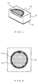
- Fig.1 shows a partially cutaway perspective view of a conventional photodiode
- Fig.2 illustrates a plan view thereof.
- An impurity diffused region (or an active region) 10 formed in a substrate 8 is shown by a hatching area.
- An annular electrode 12 is formed on the top of the diffused region 10, and a flat electrode 6 is formed on the bottom of the substrate 8.
- the carriers generated in the active region are accelerated by reverse vias applied to the PN junction to cause a drift current.
- the carriers generated in the area outside the active region cause a diffusion current.
- the diffusion current has an influence on the output of the photodiode. That is, when a part of light is absorbed in the area outside the active region, the output of the photodiode with respect to the light input is decreased. Also, the carriers generated in the active region and then overflowed into the area outside the active region, and the carriers generated in the area outside the active region are diffused and recombinated in delayed. This causes the phenomenon such that the following-up to pulsed light is delayed, and then the photoelectric conversion for a highspeed digital signal may not be effectively performed. The phenomenon are generally referred to as "a slow tail phenomenon" in the output in a photodiode, resulting in bit errors.
- a floating guard ring method In order to suppress the occurrence of such a slow tail phenomenon, the following methods are used, i.e. (1) a floating guard ring method, and (2) a method for shielding light by using a metal film and the like.
- a floating guard ring 14 is provided in a region surrounding the active region 10.
- the floating guard ring 14 is formed by diffusing an impurity in a substrate in the same manner as the formation of the active region 10. Therefore, the floating guard ring also includes a PN junction.
- the internal electric field caused in the PN junction promotes the recombination of generated carriers to suppress the slow tail phenomenon.
- the area outside the active region 10 is covered by a light shielding film 16 in order to prevent light from impinging upon the area.
- the electric field between the active region 10 and the floating guard ring 14 is zero. Therefore, when light impinges upon between the active region 10 and the floating guard ring 14, the carriers generated therebetween migrate to the active region 10 or the floating guard ring 14 by diffusion.
- the carriers reached to the floating guard ring are not necessarily combinated therein as described above. Accordingly, the float guard ring method may not suppress enough the slow tail phenomenon.
- the method for shielding light by using a metal film and the like is effective to the insufficiency of convergence of light and the optical misalignment, but is not effective to the reflection and scattering of light passing through the active region on the bottom electrode, and the overflow of carriers from the active region to the area outside the active region.
- the light shielding film 16 may prevent light from impinging, but have no effect on the prevention for mutual diffusion of carriers between the active region and the area outside the active region.
- the optical fiber When an optical fiber is coupled to the conventional photodiode, the optical fiber is aligned to the photodiode while outputting light from the optical fiber and monitoring the output of the photodiode.
- There are two methods for such alignment i.e. one is a DC alignment method in which an optical fiber is aligned to a photodiode so that the output of the photodiode becomes maximum while outputting continuous light (DC light) the strength thereof does not varied from the optical fiber, and the other is an AC alignment method using AC light the strength thereof is varied periodically.
- DC alignment method continuous light
- the carriers generated in the area outside the active region are diffused into the active region to contribute the output of a photodiode in the case of DC light, while in the case of AC light, the diffusion of carriers may not follow with the variation of the strength of AC light when the frequency thereof is high. Therefore, the output of the photodiode in the case of AC light is different from that in the case of DC light. Accordingly, the results of alignment are different in the DC alignment and AC alignment methods depending on the state of carriers generated in the area outside the active region.
- An object of the present invention is to provide a semiconductor light-receiving element fabricated by using an impurity diffusion, in which a slow tail phenomenon caused in the processing of a digital signal may be suppressed.
- Another object of the present invention is to provide a semiconductor light-receiving element in which when an optical 'fiber is coupled thereto, the optimum alignment position has no difference between a DC alignment and AC alignment.
- the present invention provides a semiconductor light-receiving element, comprising :
- the present invention provides a method for coupling an optical fiber with the semiconductor light-receiving element according to claim 1 or 2, comprising the steps of :
- Fig.5 shows a plan view of a photodiode of a first embodiment according to the present invention.
- This photodiode further comprises an annular guard ring 18 surrounding the active region 10 in the conventional photodiode as shown in Figs.1 and 2. It should be noted that in the Fig.5 like reference numerals are used for like elements in Figs. 1 and 2.
- the annular guard ring 18 is formed by an impurity diffused region, and a circular electrode 20 is provided thereon. In order to cause the guard ring 18 to be electrically independent of the active region 10, it is required to leave a certain space therebetween.
- a PN junction surrounding the active region 10 is formed in the guard ring 18, and a reverse vias is applied to the PN junction by the electrode 20.
- a reverse vias is applied to the PN junction by the electrode 20.
- Fig.6 shows a graph illustrating the effect of the present embodiment.
- an ordinate designates a relative output of the photodiode
- an abscissa denotes a time.
- a curve 30 shows a characteristic of the conventional photodiode shown in Figs.1 and 2, and a curve 32 that of the conventional photodiode according to the floating guard ring method shown in Fig.3, and a curve 34 that of the photodiode of the present embodiment.
- the conventional photodiode according to the floating guard ring method of the curve 32 decrease its slow tail to fractions of that of the conventional photodiode of the curve 30, and the photodiode of the present embodiment of the curve 34 further decrease its slow tail to more than one-half of that of the photodiode of the curve 32.
- a space more than a certain value between the active region and the guard ring is required to make the guard ring independent of the active region. Therefore, if light impinges upon an impurity non-diffused region between the active region and the guard ring, then a diffusion current flows in that region, resulting in a factor of a slow tail phenomenon.
- a light shielding film such as a metal film may be provided on the region.
- the photodiode including such light shielding film is illustrated in a plan view of Fig. 7.
- the photodiode is provided with a light shielding film 22 covering the non-diffused region between the active region 10 and guard ring 18, in the photodiode in Fig.5.
- the factor of a slow tail phenomenon is eliminated in the photodiode in Fig.5, so that the characteristic thereof may be further improved.
- the light shielding film is provided only on the impurity non-diffused region between the active region 10 and the annular guard ring 18. Therefore, if light impinges upon an impurity non-diffused region outside the annular guard ring 18, then a diffusion current generated in the non-diffused region causes the factor of a slow tail phenomenon.
- a photodiode of a third embodiment there is shown a photodiode of a third embodiment.
- a light shielding film 24 is provided not only on the impurity non-diffused region between the active region 10 and the annular guard ring 18 but also on the guard ring 18 except the electrode 20 and on the impurity non-diffused region outside the guard ring 18.
- the problems of both the insufficiency of convergence of light and the optical misalignment may be solved by means of the light shielding film 24.
- the carriers are recombinated by drift in the guard ring region 18, the carriers being generated by the light passed through the active region 10 and then reflected or scattered on the bottom electrode, and being generated in the active region 10 and overflown outside thereof. Therefore, further improvement of the characteristic of the photodiode may be realized.
- This embodiment is directed to a method for coupling an optical fiber and the diode of the first or second embodiment.
- the annular guard ring 18 of the present invention works as an active region. Therefore, when an optical fiber is coupled with the photodiode, the optical fiber may be aligned with the photodiode by monitoring the outputs from both the active region 10 and the guard ring 18 while outputting light from the optical fiber.
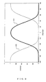
- Fig.9 shows a graph illustrating the outputs monitored. An ordinate designates the magnitude of the output, and an abscissa a position of the optical fiber with respect to the photodiode.
- the thick line 40 denotes the output of the active region 10, and the thin line the output of the guard ring 18.
- the alignment position to be targeted corresponds to that where the output of the guard ring 18 is smallest and the output of the active region 10 is largest.
- the alignment between the photodetector and the optical fiber becomes easier.
- the carriers generated in the area outside the active region may be prevented from diffusing into the active region. Therefore, the difference may not be caused in the optimum alignment positions by the DC and AC alignments.
Landscapes
- Light Receiving Elements (AREA)
- Optical Couplings Of Light Guides (AREA)
- Solid State Image Pick-Up Elements (AREA)
Abstract
Description
Claims (6)
- A semiconductor light-receiving element, comprising :wherein a reverse vias is applied to a PN junction formed by the substrate and the second impurity diffused region.a substrate including a first impurity diffused region,a first electrode provided on the bottom of the substrate,a second electrode provided on the first impurity diffused region,a second impurity diffused region provided so as to surround the first impurity diffused region with leaving a certain space therebetween, anda third electrode provided on the second impurity diffused region,
- The semiconductor light-receiving element according to claim 1, wherein a light shielding film is provided on an impurity non-diffused region between the first and second impurity diffused regions.
- The semiconductor light-receiving element according to claim 1, wherein a light shielding film is provided on the surface of the semiconductor light-receiving element except the first impurity diffused region and the third electrode.
- The semiconductor light-receiving element according to claim 2 or 3, wherein the light shielding film is a metal film.
- The semiconductor light-receiving element according to claim 4, wherein the semiconductor light-receiving element is a photodiode.
- A method for coupling an optical fiber with the semiconductor light-receiving element according to claim 1 or 2, comprising the steps of :shifting an end of the optical fiber with respect to the first impurity diffused region of the semiconductor light-receiving element while outputting light from the optical fiber,monitoring the outputs of the first and second impurity diffused regions, anddetermining optimum alignment position of the optical fiber with respect to the semiconductor light-receiving element, when the output of the first impurity diffused region is largest and the output of the second impurity diffused region is smallest.
Applications Claiming Priority (2)
| Application Number | Priority Date | Filing Date | Title |
|---|---|---|---|
| JP2000181222 | 2000-06-16 | ||
| JP2000181222A JP2001358359A (en) | 2000-06-16 | 2000-06-16 | Semiconductor light receiving element |
Publications (2)
| Publication Number | Publication Date |
|---|---|
| EP1178541A2 true EP1178541A2 (en) | 2002-02-06 |
| EP1178541A3 EP1178541A3 (en) | 2003-07-09 |
Family
ID=18682189
Family Applications (1)
| Application Number | Title | Priority Date | Filing Date |
|---|---|---|---|
| EP01114398A Withdrawn EP1178541A3 (en) | 2000-06-16 | 2001-06-14 | Semiconductor light-receiving element |
Country Status (3)
| Country | Link |
|---|---|
| US (1) | US6507084B2 (en) |
| EP (1) | EP1178541A3 (en) |
| JP (1) | JP2001358359A (en) |
Families Citing this family (5)
| Publication number | Priority date | Publication date | Assignee | Title |
|---|---|---|---|---|
| JP3907542B2 (en) * | 2002-07-16 | 2007-04-18 | シャープ株式会社 | Optical communication module |
| US8049293B2 (en) * | 2005-03-07 | 2011-11-01 | Sony Corporation | Solid-state image pickup device, electronic apparatus using such solid-state image pickup device and method of manufacturing solid-state image pickup device |
| US20070262296A1 (en) * | 2006-05-11 | 2007-11-15 | Matthias Bauer | Photodetectors employing germanium layers |
| CN105428430A (en) * | 2015-12-18 | 2016-03-23 | 四川钟顺太阳能开发有限公司 | Multi-junction GaAs solar cell surface grid line structure |
| KR102588651B1 (en) | 2020-11-12 | 2023-10-12 | 한국표준과학연구원 | Light detection device and method for manufacturing the same |
Family Cites Families (6)
| Publication number | Priority date | Publication date | Assignee | Title |
|---|---|---|---|---|
| US3995303A (en) * | 1975-06-05 | 1976-11-30 | Bell Telephone Laboratories, Incorporated | Growth and operation of a step-graded ternary III-V heterojunction p-n diode photodetector |
| JPS60182778A (en) * | 1984-02-29 | 1985-09-18 | Fujitsu Ltd | Semiconductor light receiving device |
| JPH03220782A (en) * | 1990-01-25 | 1991-09-27 | Mitsubishi Electric Corp | Semiconductor light receiving device |
| US5345075A (en) * | 1990-11-13 | 1994-09-06 | Sumitomo Electric Industries, Ltd. | Semiconductor photodetector with dielectric shielding |
| US5365087A (en) * | 1992-07-15 | 1994-11-15 | Sumitomo Electric Industries, Ltd. | Photodetector and opto-electronic integrated circuit with guard ring |
| JP3221402B2 (en) * | 1998-06-22 | 2001-10-22 | 住友電気工業株式会社 | Light receiving element and light receiving device |
-
2000
- 2000-06-16 JP JP2000181222A patent/JP2001358359A/en active Pending
-
2001
- 2001-06-13 US US09/880,298 patent/US6507084B2/en not_active Expired - Fee Related
- 2001-06-14 EP EP01114398A patent/EP1178541A3/en not_active Withdrawn
Also Published As
| Publication number | Publication date |
|---|---|
| JP2001358359A (en) | 2001-12-26 |
| US20010052630A1 (en) | 2001-12-20 |
| US6507084B2 (en) | 2003-01-14 |
| EP1178541A3 (en) | 2003-07-09 |
Similar Documents
| Publication | Publication Date | Title |
|---|---|---|
| CA2050362C (en) | Photo-sensing device | |
| US9276162B2 (en) | Semiconductor photodetector and method for manufacturing the same | |
| US5040039A (en) | Semiconductor photodetector device | |
| US5412229A (en) | Semiconductor light detecting device making use of a photodiode chip | |
| KR960001190B1 (en) | Photo-detector | |
| KR950003950B1 (en) | Photo-sensing device | |
| JPH04505233A (en) | Avalanche photodiode | |
| CN112201723A (en) | A kind of waveguide type photodetector and preparation method thereof | |
| JPH0799778B2 (en) | Backlighted photodiode with wide bandgear capping layer. | |
| KR950004550B1 (en) | Light receiving element | |
| US6507084B2 (en) | Semiconductor light-receiving element | |
| US6798001B2 (en) | Semiconductor device having photo diode with sensitivity to light of different wavelengths | |
| JP2002314116A (en) | Lateral semiconductor photodetector with PIN structure | |
| US5272364A (en) | Semiconductor photodetector device with short lifetime region | |
| JPS6244867B2 (en) | ||
| KR100676733B1 (en) | UV detector with NIP structure | |
| CN112271229A (en) | Silicon-based back-illuminated PIN device structure | |
| EP0346901A2 (en) | Semiconductor photodetector | |
| CN121888700A (en) | Photoelectric conversion element | |
| KR890004430B1 (en) | Photodiode Structure | |
| JPS6129180A (en) | Semiconductor photodetector | |
| JPS6384169A (en) | Optical semiconductor device | |
| KR100654310B1 (en) | P layer carrier and N layer carrier intrinsic semiconductor diffusion prevention method of optical detector | |
| Purica et al. | Design and optimization of InGaAs/InP photodetector for coordinate sensitive detection systems | |
| JPS62186574A (en) | Semiconductor light receiving device |
Legal Events
| Date | Code | Title | Description |
|---|---|---|---|
| PUAI | Public reference made under article 153(3) epc to a published international application that has entered the european phase |
Free format text: ORIGINAL CODE: 0009012 |
|
| AK | Designated contracting states |
Kind code of ref document: A2 Designated state(s): AT BE CH CY DE DK ES FI FR GB GR IE IT LI LU MC NL PT SE TR |
|
| AX | Request for extension of the european patent |
Free format text: AL;LT;LV;MK;RO;SI |
|
| RIN1 | Information on inventor provided before grant (corrected) |
Inventor name: NAGATA, HISAO C/O NIPPON SHEET GLASS CO., LTD. |
|
| PUAL | Search report despatched |
Free format text: ORIGINAL CODE: 0009013 |
|
| AK | Designated contracting states |
Designated state(s): AT BE CH CY DE DK ES FI FR GB GR IE IT LI LU MC NL PT SE TR |
|
| AX | Request for extension of the european patent |
Extension state: AL LT LV MK RO SI |
|
| RIC1 | Information provided on ipc code assigned before grant |
Ipc: 7G 02B 6/42 B Ipc: 7H 01L 31/103 B Ipc: 7H 01L 31/0224 A |
|
| AKX | Designation fees paid | ||
| REG | Reference to a national code |
Ref country code: DE Ref legal event code: 8566 |
|
| STAA | Information on the status of an ep patent application or granted ep patent |
Free format text: STATUS: THE APPLICATION IS DEEMED TO BE WITHDRAWN |
|
| 18D | Application deemed to be withdrawn |
Effective date: 20040110 |