EP1178042A1 - -diketonato-metal complexes and process for the preparation thereof, photoelectric conversion devices and photoelectrochemical cells - Google Patents
-diketonato-metal complexes and process for the preparation thereof, photoelectric conversion devices and photoelectrochemical cells Download PDFInfo
- Publication number
- EP1178042A1 EP1178042A1 EP00985899A EP00985899A EP1178042A1 EP 1178042 A1 EP1178042 A1 EP 1178042A1 EP 00985899 A EP00985899 A EP 00985899A EP 00985899 A EP00985899 A EP 00985899A EP 1178042 A1 EP1178042 A1 EP 1178042A1
- Authority
- EP
- European Patent Office
- Prior art keywords
- group
- atom
- metal complex
- acid
- diketonate
- Prior art date
- Legal status (The legal status is an assumption and is not a legal conclusion. Google has not performed a legal analysis and makes no representation as to the accuracy of the status listed.)
- Granted
Links
- 0 CC(C)(CCC1*C1)C1CCCC1 Chemical compound CC(C)(CCC1*C1)C1CCCC1 0.000 description 3
Images

Classifications
-
- H—ELECTRICITY
- H01—ELECTRIC ELEMENTS
- H01M—PROCESSES OR MEANS, e.g. BATTERIES, FOR THE DIRECT CONVERSION OF CHEMICAL ENERGY INTO ELECTRICAL ENERGY
- H01M14/00—Electrochemical current or voltage generators not provided for in groups H01M6/00 - H01M12/00; Manufacture thereof
- H01M14/005—Photoelectrochemical storage cells
-
- C—CHEMISTRY; METALLURGY
- C07—ORGANIC CHEMISTRY
- C07F—ACYCLIC, CARBOCYCLIC OR HETEROCYCLIC COMPOUNDS CONTAINING ELEMENTS OTHER THAN CARBON, HYDROGEN, HALOGEN, OXYGEN, NITROGEN, SULFUR, SELENIUM OR TELLURIUM
- C07F15/00—Compounds containing elements of Groups 8, 9, 10 or 18 of the Periodic Table
- C07F15/0006—Compounds containing elements of Groups 8, 9, 10 or 18 of the Periodic Table compounds of the platinum group
- C07F15/0046—Ruthenium compounds
- C07F15/0053—Ruthenium compounds without a metal-carbon linkage
-
- H—ELECTRICITY
- H01—ELECTRIC ELEMENTS
- H01G—CAPACITORS; CAPACITORS, RECTIFIERS, DETECTORS, SWITCHING DEVICES, LIGHT-SENSITIVE OR TEMPERATURE-SENSITIVE DEVICES OF THE ELECTROLYTIC TYPE
- H01G9/00—Electrolytic capacitors, rectifiers, detectors, switching devices, light-sensitive or temperature-sensitive devices; Processes of their manufacture
- H01G9/20—Light-sensitive devices
-
- H—ELECTRICITY
- H01—ELECTRIC ELEMENTS
- H01G—CAPACITORS; CAPACITORS, RECTIFIERS, DETECTORS, SWITCHING DEVICES, LIGHT-SENSITIVE OR TEMPERATURE-SENSITIVE DEVICES OF THE ELECTROLYTIC TYPE
- H01G9/00—Electrolytic capacitors, rectifiers, detectors, switching devices, light-sensitive or temperature-sensitive devices; Processes of their manufacture
- H01G9/20—Light-sensitive devices
- H01G9/2027—Light-sensitive devices comprising an oxide semiconductor electrode
- H01G9/2031—Light-sensitive devices comprising an oxide semiconductor electrode comprising titanium oxide, e.g. TiO2
-
- H—ELECTRICITY
- H10—SEMICONDUCTOR DEVICES; ELECTRIC SOLID-STATE DEVICES NOT OTHERWISE PROVIDED FOR
- H10K—ORGANIC ELECTRIC SOLID-STATE DEVICES
- H10K85/00—Organic materials used in the body or electrodes of devices covered by this subclass
- H10K85/30—Coordination compounds
- H10K85/341—Transition metal complexes, e.g. Ru(II)polypyridine complexes
- H10K85/344—Transition metal complexes, e.g. Ru(II)polypyridine complexes comprising ruthenium
-
- H—ELECTRICITY
- H10—SEMICONDUCTOR DEVICES; ELECTRIC SOLID-STATE DEVICES NOT OTHERWISE PROVIDED FOR
- H10K—ORGANIC ELECTRIC SOLID-STATE DEVICES
- H10K30/00—Organic devices sensitive to infrared radiation, light, electromagnetic radiation of shorter wavelength or corpuscular radiation
- H10K30/10—Organic devices sensitive to infrared radiation, light, electromagnetic radiation of shorter wavelength or corpuscular radiation comprising heterojunctions between organic semiconductors and inorganic semiconductors
- H10K30/15—Sensitised wide-bandgap semiconductor devices, e.g. dye-sensitised TiO2
- H10K30/151—Sensitised wide-bandgap semiconductor devices, e.g. dye-sensitised TiO2 the wide bandgap semiconductor comprising titanium oxide, e.g. TiO2
-
- Y—GENERAL TAGGING OF NEW TECHNOLOGICAL DEVELOPMENTS; GENERAL TAGGING OF CROSS-SECTIONAL TECHNOLOGIES SPANNING OVER SEVERAL SECTIONS OF THE IPC; TECHNICAL SUBJECTS COVERED BY FORMER USPC CROSS-REFERENCE ART COLLECTIONS [XRACs] AND DIGESTS
- Y02—TECHNOLOGIES OR APPLICATIONS FOR MITIGATION OR ADAPTATION AGAINST CLIMATE CHANGE
- Y02E—REDUCTION OF GREENHOUSE GAS [GHG] EMISSIONS, RELATED TO ENERGY GENERATION, TRANSMISSION OR DISTRIBUTION
- Y02E10/00—Energy generation through renewable energy sources
- Y02E10/50—Photovoltaic [PV] energy
- Y02E10/542—Dye sensitized solar cells
-
- Y—GENERAL TAGGING OF NEW TECHNOLOGICAL DEVELOPMENTS; GENERAL TAGGING OF CROSS-SECTIONAL TECHNOLOGIES SPANNING OVER SEVERAL SECTIONS OF THE IPC; TECHNICAL SUBJECTS COVERED BY FORMER USPC CROSS-REFERENCE ART COLLECTIONS [XRACs] AND DIGESTS
- Y02—TECHNOLOGIES OR APPLICATIONS FOR MITIGATION OR ADAPTATION AGAINST CLIMATE CHANGE
- Y02P—CLIMATE CHANGE MITIGATION TECHNOLOGIES IN THE PRODUCTION OR PROCESSING OF GOODS
- Y02P70/00—Climate change mitigation technologies in the production process for final industrial or consumer products
- Y02P70/50—Manufacturing or production processes characterised by the final manufactured product
Definitions
- the present invention relates to a metal complex having a ⁇ -diketonate, a process for producing the same, a photoelectric conversion element, and a photochemical cell.
- Inorganic semiconductors such as a monocrystal, polycrystal, and amorphous silicon, are used as photoelectric conversion materials used for solar cells. These materials are pointed out to have the problems that they require large energy in a production process and contain components that are not environmentally preferable. To deal with these problems, an energy converter utilizing a photoelectric chemical reaction that takes place at the boundary between a photo-semiconductor and an electrolytic solution, has been developed. Titanium oxide used in the device is stable photoelectrochemically, and superior as an electrode material of a metal oxide semiconductor. However, titanium oxide has an inferior spectrum matching sunlight, and it is not expected to have high efficiency, because it has a bandgap as large as 3.0 eV.
- an organic dye is utilized to be adsorbed onto the surface of titanium oxide, to sensitize it. It is known that the adsorbed dye has a sensitizing effect, and that titanium dioxide which has a large specific surface area as the electrode of a photo-semiconductor, is used to improve the efficiency of utilization of light (JP-A-1-220380 ("JP-A" means unexamined published Japanese patent application.)). Also, it is known to use a thin film of titanium dioxide having micropores on the surface thereof (JP-A-8-99041). However, titanium dioxide has a large forbidden band and therefore cannot absorb light in the visible region. It is therefore necessary to coat titanium dioxide with a photosensitizer that absorbs light in a wavelength range in 300 to 2000 nm, to aim at sunlight, and an organic dye is used for this purpose.
- JP-A-11-144772 and JP-T-7-500630 JP-T-7-500630
- JP-T means a publication of the translation of an international patent application.
- An object of the present invention is to provide a dye having high light absorbance over a wide wavelength range. Another object of the present invention is to provide a photoelectric conversion element using the dye. A further object of the present invention is to provide a photochemical cell using the element.
- the inventors of the present invention having made earnest studies on the above objects, developed a dye which is composed of a novel ⁇ -diketonate metal complex and found that light in a wide wavelength range (less than 800 nm) can be absorbed by this dye, to complete the present invention.
- FIG. 1 is a schematic view showing the layer structure of a preferred photochemical cell according to the present invention.
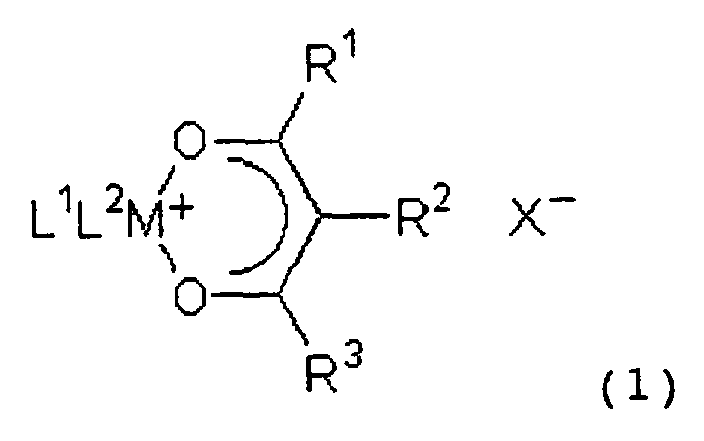
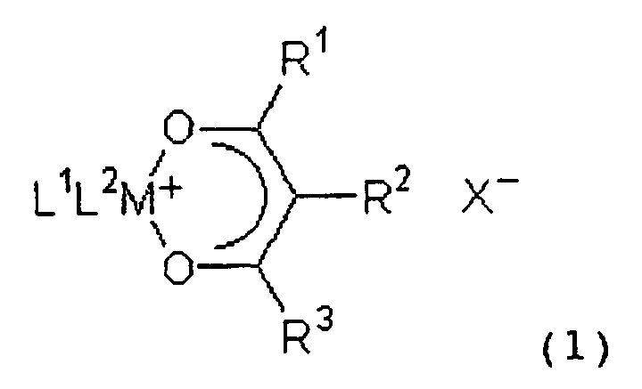
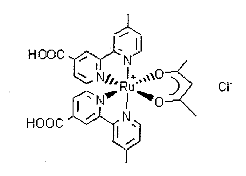
- a novel metal complex of the present invention is a metal complex having the following structure and two types of ⁇ -diketonate.
- the metal of the above metal complex is a metal of the VIII group.
- Metals of the VIII group include elements of iron, cobalt, nickel, ruthenium, rhodium, palladium, osmium, iridium and platinum.
- As the metal of the metal complex a metal which is properly selected from these VIII group metals may be used.
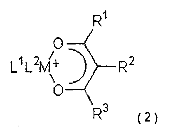
- R 1 , R 2 and R 3 are groups or atoms selected from alkyl groups, aryl groups, hydroxyl groups, amino groups, aminoalkyl groups in which a part of amino group is substituted with an alkyl group), alkoxy groups, a hydrogen atom and halogen atoms.
- the alkyl group is an aliphatic saturated hydrocarbon group which may have a straight-chain or branched chain. Given as specific examples of the alkyl group are a methyl group, ethyl group, propyl group, i-propyl group and groups of n-butyl, i-butyl, sec-butyl and tert-butyl.
- the number of the carbons of the alkyl group may be optionally selected as far as it does not disturb the production of a metal complex.
- alkyl groups whose carbon number is in a range from 1 to 10 are generally selected.
- the aryl group represents a group obtained by removing one hydrogen atom from an aromatic hydrocarbon, specifically, a phenyl group, a group such as a tolyl group and xylyl group in which a phenyl group may be substituted with an alkyl group such as a methyl group or ethyl group, biphenyl group, naphthyl group, anthryl group, phenanthryl group.
- the alkoxy group is a group in which oxygen is bonded to an alkyl group and specific examples of the alkoxy group may include a methoxy group, ethoxy group, propoxy group, butoxy group, pentyloxy group and hexyloxy group.
- Specific examples of the halogen atom may include chlorine, fluorine, bromine and iodine.
- X -1 represents a negative monovalent ion.
- the halogen ion is specifically an ion of a halogen atom selected from chlorine, fluorine, bromine and iodine.
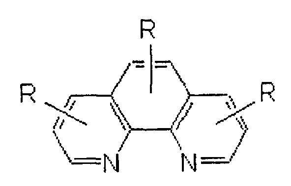
- L 1 or L 2 respectively represent a 2,2'-bipyridine group or a 1,10-phenanthroline group. These groups may be substituted with a substituent R.
- the substituent R may be substituted with a group or atom selected from an alkyl group (those having 1 to 10 carbon atoms and a straight chain or branched chain), carboxyl group, sulfonic acid group, phosphonic acid group, hydroxyl group, amino group, hydrogen atom and halogen atom.
- the substituent R may be substituted not only with one substituent but also with two or more substituents.
- R has the same meaning as defined in R 1 , R 2 or R 3 of the above-mentioned ⁇ -diketonate.
- a process for producing the metal complex having a ⁇ -diketonate represented by the above formula (1) is explained below.
- a process for producing a metal complex having a ⁇ -diketonate shown by the following formula (1) the process comprising heating a metal complex of the VIII group having, as a ligand, L 1 L 2 which represent a 2,2'-bipyridine group or a 1,10-phenanthroline group (these groups may be substituted with a group or an atom selected from an alkyl group, a carboxyl group, a sulfonic acid group, a phosphonic acid group, a hydroxyl group, an amino group, a hydrogen atom and a halogen atom) and a ⁇ -diketone derivative in the presence of an alkali and a solvent, and then treating the resulting product with an aqueous solution containing an acid.
- the raw material is a metal complex of the VIII group having, as a ligand, a group containing L 1 L 2 which represent a 2,2'-bipyridine group or a 1,10-phenanthroline group (these groups may be substituted with a group or an atom selected from an alkyl group, a carboxyl group, a sulfonic acid group, a phosphonic acid group, a hydroxyl group, an amino group, a hydrogen atom and a halogen atom), and a ⁇ -diketone or its derivative. All these compounds are known compounds.
- ruthenium, iron, cobalt, nickel, palladium or platinum can be used.
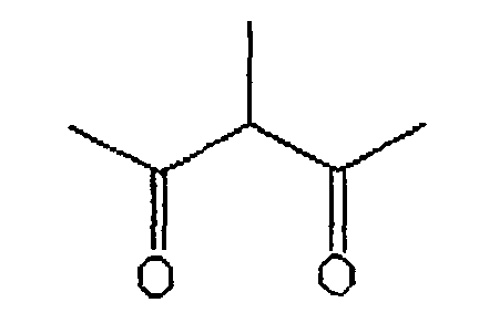
- ⁇ -diketone may include acetylacetone.
- R has the same meaning as defined in R 1 , R 2 or R 3 of the above-mentioned ⁇ -diketonate.
- the solvent may be any one of those which can solubilize the metal complex and specific examples of the solvent may include water, a mixture of dimethylformamide and water and alcohol.
- the alkali is used to generate the ⁇ -diketonate which is an anionic type and, specifically, sodium carbonate, sodium hydroxide, sodium alkoxide or the like can be used as the alkali.
- the acid used in the above reaction serves to neutralize the reaction system and to add an ion X to the complex obtained.
- X is a group selected from a halide ion, nitric acid ion, sulfonic acid ion, fluoroboric acid ion, fluorophosphoric acid ion and perchloric acid ion.
- the acid is acids having these Xs.
- the acid may include hydrochloric acid, hydrofluoric acid, hydrobromic acid, nitric acid, trifluoromethanesulfonic acid, toluenesulfonic acid, tetrafluoroboric acid, hexafluorophosphoric acid and perchloric acid.
- the object product to be obtained is a ruthenium metal complex
- R 2 is a hydrogen atom
- X - is a perchloric acid ion
- VIII group metal complex cis-dichlorobis(2,2'-bipyridine-4,4'-dicarboxylic acid) ruthenium is used and as the ⁇ -diketone, acetylacetone is used.
- a metal complex cis-dichlorobis(2,2'-bipyridine-4,4'-dicarboxylic acid) ruthenium is dissolved in a solvent to use.
- a solvent any one of those which can dissolve the above-mentioned VIII group metal complex can be optionally used.
- a mixed solvent of dimethylformamide and water etc. can be used.
- alkali any one of those which can produce the ⁇ -diketonate can be optionally utilized. Specific examples of the alkali may include sodium carbonate.
- Heating is required for the reaction and therefore the raw materials are heated under reflux.
- the product obtained with the above-mentioned treatments is dried, and an aqueous perchloric acid solution which is an aqueous solution containing X - is added to the dried product to run a reaction. After that, when the reaction mixture is put in an acidic condition, a precipitate is produced. The precipitate is separated by filtration and washed with methanol, followed by drying, and the object product can be obtained.
- the metal complex containing the ⁇ -diketonate represented by the above-described formula (1) is produced and the resulting compound is treated by a base to produce the metal complex.
- a base sodium. hydroxide and ammonia may be given.
- the product obtained in the stage prior to the treatment using the aqueous solution containing X - can be used.
- the photoelectric conversion element of the present invention is formed with forming an oxide semiconductor layer on a conductive substrate which is composed of a conductive material and adsorbing the above-mentioned metal complex having the ⁇ -diketonate of the present invention to the oxide semiconductor layer.
- a metal, carbon, conductive polymer or conductive glass can be used as the conductive material. These materials can be used whether they are light-transmittable or not.
- conductive materials having a light-transmittance of 80% or more are preferably used in general. Conductive materials having a plate-like form or a sheet-like form can be used. These materials act as a support.
- a film of a conductive metal oxide made of tin oxide or indium/tin complex oxide can be formed on the surface of glass to use.
- a conductive layer of a metal or carbon may be formed on conductive substrate to use. It is preferable that the surface resistance of the conductive substrate is generally a value of 10 ⁇ /cm 2 or less.
- a dispersion solution in which a fine particle of the oxide semiconductor is dispersed in a solvent is produced, and this dispersion solution is allowed to adhered to the surface of the conductive material, followed by baking, to form a thin film composed of the oxide semiconductor.
- an oxide of a transition metal such as titanium, niobium, zinc, tin, zirconium, yttrium, lanthanum or tantalum is used.
- Perovskite type oxides such as strontium titanate and calcium titanate can be also used. These semiconductors bring about very preferable results.
- the particle diameter is in a range from generally 1 to 5000 nm and preferably 2 to 50 nm.
- any one of solvents which can be dispersed each of these oxide semiconductors can be optionally used.
- a solvent selected from water, an organic solvent, and water and an organic solvent can be used.
- an organic solvent a hydrocarbon, alcohol, ether, ketone, ester or the like can be used.
- various surfactants and a viscosity modifier can be used.
- the viscosity modifier polyethylene glycol can be given.
- the oxide semiconductor layer is baked in the presence of air in the condition of a temperature of 1000°C or less.
- a temperature range between generally 300 and 800°C and preferably 400 and 600°C is adopted.
- the layer which is composed of the oxide semiconductor a layer which has about 5 to 100 ⁇ m as thickness after baked is required.
- the oxide semiconductor layer obtained in this manner form a fine porous layer.
- the oxide semiconductor layer formed on the above-mentioned conductive substrate is immersed in the dye dissolved in a solvent, so that a dye composed of the above-mentioned metal complex having the ⁇ -diketonate in the present invention is allowed to adsorb to the semiconductor oxide layer.
- a solvent for the dye methanol, acetonitrile, dimethylformamide, water or the like can be used.
- concentration of the dye in the solvent is appropriately selected from the range from 10 -5 to 10 -2 M to use. An optimum concentration differs depending upon the type of dye.
- the immersing time is in a range from generally 0.5 to 24 hours and is appropriately selected within the order of this range according to the need.
- a temperature ranging from room temperature to 100°C is appropriately selected in general.
- the photocell of the present invention will be explained with reference to FIG. 1.
- the photocell is composed of a counter electrode formed on the surface of a conductive substrate 1, and it is further constituted by a layer structure thereon comprising a thin film layer composed of a dye-carrying oxide semiconductor film 2, which is formed by absorbing a dye to an oxide semiconductor, a charge-transfer layer 3, and a counter electrode 4.
- the counter electrode one obtained by forming a thin layer of platinum, rhodium, ruthenium, ruthenium oxide or carbon etc. on a conductive material or a conductive substrate is used.
- a layer formed with an electrolytic solution containing a redox material in an organic solvent is used.
- a redox material a combination of, for example, I - /I 3 - , Br - /Br 3 - , Fe 2+ /Fe 3+ , Sn 2+ /Sn 4+ , Cr 2+ /Cr 3+ , V 2+ /V 3+ or quinone/hydroquinone is used.
- acetonitrile acetonitrile, propionitrile, ethylene carbonate and propylene carbonate may be given.
- this charge transfer layer a gel electrolyte obtained by solidifying the electrolytic solution of the liquid charge-transfer layer which is composed of the above-mentioned electrolytic solution, or a solid high-molecular electrolyte containing a redox substance in a high molecular substance can be used.
- the metal complex which is obtained according to the present invention and has the ⁇ -diketonate as a ligand is a dye which is composed of a metal complex exhibiting high light absorbance in the visible radiation region. Utilizing this characteristic, a photoelectric conversion element which makes use of visible rays can be obtained. The photochemical cell using this photoelectric conversion element exhibits a high photoelectric conversion efficiency.
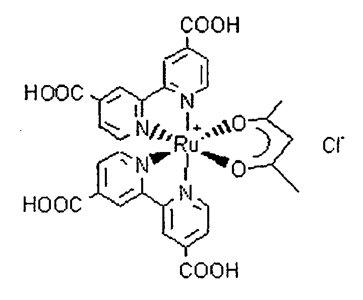
- M was a ruthenium metal
- L 1 and L 2 were both 2,2'-bipyridine-4,4'-dicarboxylic acids
- R 1 and R 3 were methyl groups
- R 2 was a hydrogen atom
- X - was a perchloric acid ion.
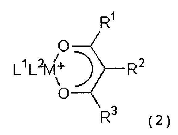
- Example 2 The product obtained in the above Example 1 was suspended in water, to which was then added an aqueous concentrated ammonia solution. The resulting solution was dried to obtain a target ruthenium complex containing a ⁇ -diketonate.
- M was a ruthenium metal
- L1 and L2 were both ammonium-2,2'-bipyridine-4,4'-dicarboxylic acids
- R 1 and R 3 were methyl groups
- R 2 was a hydrogen atom.
- Example 3 production of a photoelectric conversion element
- a conductive glass substrate SnO 2 , 10 ⁇ /cm 2
- the photochemical cell thus obtained was irradiated with pseudo sun light (1,000 w/m 2 ) using a solar simulator (manufactured by WACOM Co., Ltd.) to obtain a photocurrent of 13.2 mA/cm 2 , a photovoltage of 0.74 V and a photoelectric conversion efficiency of 6.0%.
- the metal complex containing the ⁇ -diketonate as a ligand which is obtained according to the present invention is a dye which is composed of a metal complex exhibiting high light absorbance in the visible radiation region and is therefore a suitable material to obtain a photoelectric conversion element utilizing visible rays by making use of these characteristics.
- a photochemical cell using this photoelectric conversion element exhibits a high photoelectric conversion efficiency.
Landscapes
- Chemical & Material Sciences (AREA)
- Engineering & Computer Science (AREA)
- Power Engineering (AREA)
- Organic Chemistry (AREA)
- Microelectronics & Electronic Packaging (AREA)
- General Chemical & Material Sciences (AREA)
- Electrochemistry (AREA)
- Chemical Kinetics & Catalysis (AREA)
- Crystallography & Structural Chemistry (AREA)
- Inorganic Chemistry (AREA)
- Materials Engineering (AREA)
- Hybrid Cells (AREA)
- Photovoltaic Devices (AREA)
- Pyridine Compounds (AREA)
- Organic Low-Molecular-Weight Compounds And Preparation Thereof (AREA)
Abstract

Description












Claims (6)
- A metal complex having a β-diketonate represented by the following formula (1):wherein M represents a metal atom of the VIII group; R1, R2 and R3 each represent a group or an atom selected from the group consisting of an alkyl group, an aryl group, a hydroxyl group, an amino group, an alkoxy group, a hydrogen atom and a halogen atom; X-1 represents an ion selected from a halogen ion, a nitric acid ion, a sulfonic acid ion, a fluoroboric acid ion, a fluorophosphoric acid ion and a perchloric acid ion; and L1 or L2 respectively represents a 2,2'-bipyridine group or a 1,10-phenanthroline group, each of which may be substituted with a group or an atom selected from an alkyl group, a carboxyl group, a sulfonic acid group, a phosphonic acid group, a hydroxyl group, an amino group, a hydrogen atom and a halogen atom.

- A metal complex having a β-diketonate represented by the following formula (2) :wherein M represents a metal atom of the VIII group; R1, R2 and R3 each represent a group or an atom selected from the group consisting of an alkyl group, an aryl group, a hydroxyl group, an amino group, an alkoxy group, a hydrogen atom and a halogen atom; and L1 or L2 respectively represents a 2,2'-bipyridine group or a 1,10-phenanthroline group, in which one or both of L1 or L2 may be substituted with an acidic group selected from a carboxyl group, a sulfonic acid group, a phosphonic acid group and a hydroxyl group each of which is neutralized.
- A method for producing a metal complex having a β-diketonate represented by the formula (1), comprising heating a metal complex of the VIII group having, as a ligand, L1 L2 which represent a 2,2'-bipyridine group or a 1,10-phenanthroline group (these groups may be substituted with a group or an atom selected from an alkyl group, a carboxyl group, a sulfonic acid group, a phosphonic acid group, a hydroxyl group, an amino group, a hydrogen atom and a halogen atom), and a β-diketonate derivative, in the presence of an alkali and a solvent, and treating the resulting product with an aqueous solution containing an acid.
- A method for producing a metal complex having a β-diketonate represented by the formula (2), comprising adding an alkali to the aqueous solution containing the β -diketonate described in Claim 3.
- A photoelectric conversion element, which comprises a porous oxide semiconductor layer laminated on a layer composed of an electric conductor, and the metal complex as claimed in Claim 1 or 2 adsorbed to the porous oxide semiconductor layer.
- A photochemical cell, which comprises the photoelectric conversion element as claimed in Claim 5, a counter electrode, and a charge-transfer layer.
Applications Claiming Priority (3)
| Application Number | Priority Date | Filing Date | Title |
|---|---|---|---|
| JP2000069517A JP3430254B2 (en) | 2000-03-13 | 2000-03-13 | Metal complex having β-diketonate, method for producing the same, photoelectric conversion element, and photochemical cell |
| JP2000069517 | 2000-03-13 | ||
| PCT/JP2000/009254 WO2001068608A1 (en) | 2000-03-13 | 2000-12-26 | -diketonato-metal complexes and process for the preparation thereof, photoelectric conversion devices and photoelectrochemical cells |
Publications (3)
| Publication Number | Publication Date |
|---|---|
| EP1178042A1 true EP1178042A1 (en) | 2002-02-06 |
| EP1178042A4 EP1178042A4 (en) | 2002-10-16 |
| EP1178042B1 EP1178042B1 (en) | 2003-08-27 |
Family
ID=18588377
Family Applications (1)
| Application Number | Title | Priority Date | Filing Date |
|---|---|---|---|
| EP00985899A Expired - Lifetime EP1178042B1 (en) | 2000-03-13 | 2000-12-26 | Beta-diketonato-metal complexes and process for the preparation thereof, photoelectric conversion devices and photoelectrochemical cells |
Country Status (4)
| Country | Link |
|---|---|
| US (1) | US6664462B2 (en) |
| EP (1) | EP1178042B1 (en) |
| JP (1) | JP3430254B2 (en) |
| WO (1) | WO2001068608A1 (en) |
Cited By (1)
| Publication number | Priority date | Publication date | Assignee | Title |
|---|---|---|---|---|
| EP1511116A4 (en) * | 2002-06-04 | 2010-05-05 | Nippon Oil Corp | PHOTOELECTRIC TRANSDUCER |
Families Citing this family (26)
| Publication number | Priority date | Publication date | Assignee | Title |
|---|---|---|---|---|
| GB9930248D0 (en) * | 1999-12-22 | 2000-02-09 | Johnson Matthey Plc | Surface cleaner |
| WO2002001667A1 (en) * | 2000-06-29 | 2002-01-03 | Nippon Kayaku Kabushiki Kaisha | Dye-sensitized photoelectric transducer |
| JP3985040B2 (en) * | 2002-01-22 | 2007-10-03 | 独立行政法人産業技術総合研究所 | Ruthenium complex useful as sensitizer, oxide semiconductor electrode, and solar cell using the same |
| JP4269595B2 (en) * | 2002-08-23 | 2009-05-27 | トヨタ自動車株式会社 | Oxide semiconductor electrode and manufacturing method thereof |
| US7312100B2 (en) * | 2003-05-27 | 2007-12-25 | The North Carolina State University | In situ patterning of electrolyte for molecular information storage devices |
| JP2005072524A (en) * | 2003-08-28 | 2005-03-17 | Institute Of Physical & Chemical Research | Photoelectric conversion element and solar cell using the same |
| JP4485181B2 (en) * | 2003-12-05 | 2010-06-16 | シャープ株式会社 | Metal complex and dye-sensitized solar cell using the same |
| US7812251B2 (en) | 2003-10-17 | 2010-10-12 | Sharp Kabushiki Kaisha | Photosensitizing transition metal complex and its use for photovoltaic cell |
| US20060021647A1 (en) * | 2004-07-28 | 2006-02-02 | Gui John Y | Molecular photovoltaics, method of manufacture and articles derived therefrom |
| JP2009521494A (en) | 2005-12-22 | 2009-06-04 | アルコン リサーチ, リミテッド | (Indazol-5-yl) -pyrazine and (1,3-dihydroindol-2-one) -pyrazine for treating rho kinase-mediated diseases and conditions |
| US20090242027A1 (en) | 2006-07-05 | 2009-10-01 | Teruhisa Inoue | Dye-Sensitized Solar Cell |
| AR064420A1 (en) | 2006-12-21 | 2009-04-01 | Alcon Mfg Ltd | OPHTHALMIC PHARMACEUTICAL COMPOSITIONS THAT INCLUDE AN EFFECTIVE AMOUNT OF ANALOGS OF 6-AMINOIMIDAZO [1,2B] PIRIDAZINAS, USEFUL FOR THE TREATMENT OF GLAUCOMA AND / OR CONTROL THE NORMAL OR ELEVATED INTRAOCULAR PRESSURE (IOP). |
| KR101137571B1 (en) | 2008-05-12 | 2012-04-19 | 코니카 미놀타 비지니스 테크놀로지즈 가부시키가이샤 | Dye-sensitized solar cell and method for manufacturing the same |
| JP5809954B2 (en) * | 2011-12-15 | 2015-11-11 | 富士フイルム株式会社 | Photoelectric conversion element and dye-sensitized solar cell |
| JP5881578B2 (en) | 2011-12-15 | 2016-03-09 | 富士フイルム株式会社 | Metal complex dye, photoelectric conversion element, dye-sensitized solar cell, and dye solution |
| RU2513021C1 (en) * | 2012-09-04 | 2014-04-20 | Федеральное государственное бюджетное учреждение науки Институт неорганической химии им. А.В. Николаева Сибирского отделения Российской академии наук | Method of producing palladium (ii) beta-diketonate or beta-ketoiminate |
| JP2014082187A (en) | 2012-09-28 | 2014-05-08 | Fujifilm Corp | Photoelectric conversion element and dye-sensitized solar cell |
| JP5913222B2 (en) | 2012-09-28 | 2016-04-27 | 富士フイルム株式会社 | Photoelectric conversion element and dye-sensitized solar cell |
| JP6063359B2 (en) | 2012-09-28 | 2017-01-18 | 富士フイルム株式会社 | Photoelectric conversion element, dye-sensitized solar cell, metal complex dye and dye solution formed by dissolving metal complex dye |
| JP5913223B2 (en) | 2012-09-28 | 2016-04-27 | 富士フイルム株式会社 | Metal complex dye, photoelectric conversion element, dye-sensitized solar cell, dye solution and dye-adsorbing electrode |
| JP5992389B2 (en) | 2012-11-16 | 2016-09-14 | 富士フイルム株式会社 | Photoelectric conversion element, dye-sensitized solar cell, metal complex dye, dye solution, dye-adsorbing electrode, and method for producing dye-sensitized solar battery |
| JP5944372B2 (en) | 2012-12-17 | 2016-07-05 | 富士フイルム株式会社 | Photoelectric conversion element, dye-sensitized solar cell, metal complex dye, dye solution, dye-adsorbing electrode, and method for producing dye-sensitized solar battery |
| JP5972811B2 (en) | 2013-02-22 | 2016-08-17 | 富士フイルム株式会社 | Photoelectric conversion element, method for producing photoelectric conversion element, and dye-sensitized solar cell |
| JP6047513B2 (en) | 2013-03-25 | 2016-12-21 | 富士フイルム株式会社 | Metal complex dye, photoelectric conversion element, dye-sensitized solar cell, and dye solution containing metal complex dye |
| JP2016063113A (en) * | 2014-09-19 | 2016-04-25 | 株式会社東芝 | Nonvolatile semiconductor memory device |
| US20200279693A1 (en) * | 2016-05-04 | 2020-09-03 | Sogang University Research & Business Development Foundation | Dye-sensitized solar cell comprising light collecting device panel |
Family Cites Families (14)
| Publication number | Priority date | Publication date | Assignee | Title |
|---|---|---|---|---|
| NL260509A (en) * | 1960-01-26 | |||
| US3647832A (en) * | 1967-03-23 | 1972-03-07 | Rhone Poulenc Sa | Ruthenium complexes and processes for their preparation |
| CH674596A5 (en) | 1988-02-12 | 1990-06-15 | Sulzer Ag | |
| GB9217811D0 (en) | 1992-08-21 | 1992-10-07 | Graetzel Michael | Organic compounds |
| JP2636158B2 (en) | 1993-12-09 | 1997-07-30 | 工業技術院長 | Titanium oxide porous thin film photocatalyst and method for producing the same |
| JP4298799B2 (en) * | 1997-05-07 | 2009-07-22 | エコール ポリテクニーク フェデラル ドゥ ローザンヌ | Metal composite photosensitizer and photovoltaic cell |
| JP4623768B2 (en) * | 1997-06-23 | 2011-02-02 | シャープ株式会社 | Photoelectric conversion material, method for producing the same, and photoelectric conversion device |
| AU739903B2 (en) * | 1997-06-23 | 2001-10-25 | Sharp Kabushiki Kaisha | Photoelectric material using organic photosensitising dyes and manufacturing method thereof |
| JP3309785B2 (en) | 1997-11-06 | 2002-07-29 | 富士ゼロックス株式会社 | Semiconductor electrode, method of manufacturing the same, and photovoltaic cell using the same |
| JPH11167937A (en) * | 1997-09-30 | 1999-06-22 | Fuji Photo Film Co Ltd | Photoelectric transfer element |
| DE69823706T2 (en) * | 1997-10-23 | 2005-04-28 | Fuji Photo Film Co. Ltd., Minamiashigara | Photoelectric conversion assembly and photoelectrochemical cell |
| JPH11273753A (en) | 1998-03-25 | 1999-10-08 | Sekisui Chem Co Ltd | Dye-sensitized photocell |
| JP2000106223A (en) | 1998-09-29 | 2000-04-11 | Fuji Photo Film Co Ltd | Photoelectric conversion element |
| EP2280404A3 (en) * | 1999-04-26 | 2011-04-13 | FUJIFILM Corporation | Metal complex dye for a photoelectrochemical cell |
-
2000
- 2000-03-13 JP JP2000069517A patent/JP3430254B2/en not_active Expired - Lifetime
- 2000-12-26 US US09/959,949 patent/US6664462B2/en not_active Expired - Fee Related
- 2000-12-26 WO PCT/JP2000/009254 patent/WO2001068608A1/en not_active Ceased
- 2000-12-26 EP EP00985899A patent/EP1178042B1/en not_active Expired - Lifetime
Cited By (1)
| Publication number | Priority date | Publication date | Assignee | Title |
|---|---|---|---|---|
| EP1511116A4 (en) * | 2002-06-04 | 2010-05-05 | Nippon Oil Corp | PHOTOELECTRIC TRANSDUCER |
Also Published As
| Publication number | Publication date |
|---|---|
| US20020170594A1 (en) | 2002-11-21 |
| EP1178042B1 (en) | 2003-08-27 |
| JP2001253894A (en) | 2001-09-18 |
| EP1178042A4 (en) | 2002-10-16 |
| WO2001068608A1 (en) | 2001-09-20 |
| JP3430254B2 (en) | 2003-07-28 |
| US6664462B2 (en) | 2003-12-16 |
Similar Documents
| Publication | Publication Date | Title |
|---|---|---|
| EP1178042B1 (en) | Beta-diketonato-metal complexes and process for the preparation thereof, photoelectric conversion devices and photoelectrochemical cells | |
| KR101553104B1 (en) | Photoelectric conversion element, photoelectrochemical battery, dye for photoelectric conversion element, and dye solution for photoelectric conversion element | |
| Altobello et al. | Sensitization of nanocrystalline TiO2 with black absorbers based on Os and Ru polypyridine complexes | |
| JP5572029B2 (en) | Metal complex dye, photoelectric conversion element and photoelectrochemical cell | |
| JP2997773B1 (en) | Metal complexes, oxide semiconductor electrodes and solar cells useful as sensitizers | |
| EP0924724B1 (en) | Photoelectric conversion device and photo-electrochemical cell | |
| JPH0815097B2 (en) | Photocell | |
| US20120085411A1 (en) | Photoelectric conversion element and solar cell | |
| WO2012033143A1 (en) | Photoelectric conversion element, photoelectrochemical battery, and dye | |
| KR102585159B1 (en) | Manufacturing method of perovskite crystalline precursor using eco-friendly solvent and perovskite optoelectronic device using the same | |
| JP2009269987A (en) | Novel compound, photoelectric transducer and solar cell | |
| EP2272920B1 (en) | Dye for dye-sensitized solar cell and dye-sensitized solar cell including the same | |
| JP5620496B2 (en) | Metal complex dye, photoelectric conversion element and photoelectrochemical cell | |
| CN102884137B (en) | Photoelectric conversion element and photochemical cell comprising a dinuclear ruthenium complex dye having a substituted bipyridyl group | |
| TWI564301B (en) | Metal complex dye composition, photoelectric conversion element, photoelectrochemical cell, and method for producing metal complex dye | |
| WO2012017874A1 (en) | Metal complex dye, photoelectric conversion element, and photoelectrochemical cell | |
| JP5332114B2 (en) | Photoelectric conversion element and solar cell | |
| WO2012017873A1 (en) | Metal complex dye, photoelectric conversion element and photoelectrochemical cell | |
| EP2262049A1 (en) | Novel photosensitizer and photovoltaic element | |
| JP2012036239A (en) | Metal complex dye, photoelectric conversion element, and photoelectrochemical cell | |
| JP5749883B2 (en) | Dye, photoelectric conversion element and photoelectrochemical cell using the same | |
| JP2009187820A (en) | Photoelectric conversion element and solar cell | |
| JP4605111B2 (en) | Photoelectric conversion element and dye-sensitized solar cell | |
| JP2004014370A (en) | Oxide semiconductor electrode and photoelectric conversion element | |
| JP5374834B2 (en) | Dye-sensitized photoelectric conversion element and dye-sensitized solar cell |
Legal Events
| Date | Code | Title | Description |
|---|---|---|---|
| PUAI | Public reference made under article 153(3) epc to a published international application that has entered the european phase |
Free format text: ORIGINAL CODE: 0009012 |
|
| AK | Designated contracting states |
Kind code of ref document: A1 Designated state(s): BE CH LI |
|
| 17P | Request for examination filed |
Effective date: 20020121 |
|
| A4 | Supplementary search report drawn up and despatched |
Effective date: 20020830 |
|
| AK | Designated contracting states |
Kind code of ref document: A4 Designated state(s): BE CH LI |
|
| RIC1 | Information provided on ipc code assigned before grant |
Free format text: 7C 07D 213/79 A, 7C 07D 471/04 B, 7H 01M 14/00 B, 7C 07F 15/00 B, 7C 07F 15/00 J, 7C 07C 49:92 J |
|
| GRAH | Despatch of communication of intention to grant a patent |
Free format text: ORIGINAL CODE: EPIDOS IGRA |
|
| RTI1 | Title (correction) |
Free format text: BETA-DIKETONATO-METAL COMPLEXES AND PROCESS FOR THE PREPARATION THEREOF, PHOTOELECTRIC CONVERSION DEVICES AND PHOTOELECTR |
|
| GRAS | Grant fee paid |
Free format text: ORIGINAL CODE: EPIDOSNIGR3 |
|
| GRAA | (expected) grant |
Free format text: ORIGINAL CODE: 0009210 |
|
| AK | Designated contracting states |
Designated state(s): BE CH LI |
|
| REG | Reference to a national code |
Ref country code: CH Ref legal event code: EP |
|
| RAP2 | Party data changed (patent owner data changed or rights of a patent transferred) |
Owner name: NATIONAL INSTITUTE OF ADVANCED INDUSTRIAL SCIENCE |
|
| REG | Reference to a national code |
Ref country code: CH Ref legal event code: NV Representative=s name: E. BLUM & CO. PATENTANWAELTE Ref country code: CH Ref legal event code: PUE Owner name: NATIONAL INSTITUTE OF ADVANCED INDUSTRIAL SCIENCE Free format text: JAPAN AS REPRESENTED BY SECRETARY OF AGENCY OF INDUSTRIAL SCIENCE AND TECHNOLOGY#3-1 KASUMIGASEKI, 1-CHOME#CHIYODA-KU, TOKYO 100-8921 (JP) -TRANSFER TO- NATIONAL INSTITUTE OF ADVANCED INDUSTRIAL SCIENCE AND TECHNOLOGY#3-1, KASUMIGASEKI 1-CHOME, CHIYODA-KU#TOKYO 100-8921 (JP) |
|
| PLBE | No opposition filed within time limit |
Free format text: ORIGINAL CODE: 0009261 |
|
| STAA | Information on the status of an ep patent application or granted ep patent |
Free format text: STATUS: NO OPPOSITION FILED WITHIN TIME LIMIT |
|
| 26N | No opposition filed |
Effective date: 20040528 |
|
| REG | Reference to a national code |
Ref country code: CH Ref legal event code: PFA Owner name: NATIONAL INSTITUTE OF ADVANCED INDUSTRIAL SCIENCE Free format text: NATIONAL INSTITUTE OF ADVANCED INDUSTRIAL SCIENCE AND TECHNOLOGY#3-1, KASUMIGASEKI 1-CHOME, CHIYODA-KU#TOKYO 100-8921 (JP) -TRANSFER TO- NATIONAL INSTITUTE OF ADVANCED INDUSTRIAL SCIENCE AND TECHNOLOGY#3-1, KASUMIGASEKI 1-CHOME, CHIYODA-KU#TOKYO 100-8921 (JP) |
|
| PGFP | Annual fee paid to national office [announced via postgrant information from national office to epo] |
Ref country code: CH Payment date: 20091224 Year of fee payment: 10 |
|
| PGFP | Annual fee paid to national office [announced via postgrant information from national office to epo] |
Ref country code: BE Payment date: 20100212 Year of fee payment: 10 |
|
| BERE | Be: lapsed |
Owner name: NATIONAL INSTITUTE OF *ADVANCED INDUSTRIAL SCIENCE Effective date: 20101231 |
|
| REG | Reference to a national code |
Ref country code: CH Ref legal event code: PL |
|
| PG25 | Lapsed in a contracting state [announced via postgrant information from national office to epo] |
Ref country code: BE Free format text: LAPSE BECAUSE OF NON-PAYMENT OF DUE FEES Effective date: 20101231 |
|
| PG25 | Lapsed in a contracting state [announced via postgrant information from national office to epo] |
Ref country code: CH Free format text: LAPSE BECAUSE OF NON-PAYMENT OF DUE FEES Effective date: 20101231 Ref country code: LI Free format text: LAPSE BECAUSE OF NON-PAYMENT OF DUE FEES Effective date: 20101231 |