EP1176640A2 - Contact structure of an integrated power circuit - Google Patents
Contact structure of an integrated power circuit Download PDFInfo
- Publication number
- EP1176640A2 EP1176640A2 EP01000318A EP01000318A EP1176640A2 EP 1176640 A2 EP1176640 A2 EP 1176640A2 EP 01000318 A EP01000318 A EP 01000318A EP 01000318 A EP01000318 A EP 01000318A EP 1176640 A2 EP1176640 A2 EP 1176640A2
- Authority
- EP
- European Patent Office
- Prior art keywords
- layer
- transistor
- contact pads
- electrodes
- metal layer
- Prior art date
- Legal status (The legal status is an assumption and is not a legal conclusion. Google has not performed a legal analysis and makes no representation as to the accuracy of the status listed.)
- Granted
Links
Images


Classifications
-
- H—ELECTRICITY
- H10—SEMICONDUCTOR DEVICES; ELECTRIC SOLID-STATE DEVICES NOT OTHERWISE PROVIDED FOR
- H10W—GENERIC PACKAGES, INTERCONNECTIONS, CONNECTORS OR OTHER CONSTRUCTIONAL DETAILS OF DEVICES COVERED BY CLASS H10
- H10W70/00—Package substrates; Interposers; Redistribution layers [RDL]
- H10W70/40—Leadframes
- H10W70/464—Additional interconnections in combination with leadframes
- H10W70/465—Bumps or wires
-
- H—ELECTRICITY
- H10—SEMICONDUCTOR DEVICES; ELECTRIC SOLID-STATE DEVICES NOT OTHERWISE PROVIDED FOR
- H10W—GENERIC PACKAGES, INTERCONNECTIONS, CONNECTORS OR OTHER CONSTRUCTIONAL DETAILS OF DEVICES COVERED BY CLASS H10
- H10W20/00—Interconnections in chips, wafers or substrates
- H10W20/40—Interconnections external to wafers or substrates, e.g. back-end-of-line [BEOL] metallisations or vias connecting to gate electrodes
- H10W20/41—Interconnections external to wafers or substrates, e.g. back-end-of-line [BEOL] metallisations or vias connecting to gate electrodes characterised by their conductive parts
- H10W20/427—Power or ground buses
-
- H—ELECTRICITY
- H10—SEMICONDUCTOR DEVICES; ELECTRIC SOLID-STATE DEVICES NOT OTHERWISE PROVIDED FOR
- H10W—GENERIC PACKAGES, INTERCONNECTIONS, CONNECTORS OR OTHER CONSTRUCTIONAL DETAILS OF DEVICES COVERED BY CLASS H10
- H10W70/00—Package substrates; Interposers; Redistribution layers [RDL]
- H10W70/40—Leadframes
- H10W70/481—Leadframes for devices being provided for in groups H10D8/00 - H10D48/00
-
- H—ELECTRICITY
- H10—SEMICONDUCTOR DEVICES; ELECTRIC SOLID-STATE DEVICES NOT OTHERWISE PROVIDED FOR
- H10W—GENERIC PACKAGES, INTERCONNECTIONS, CONNECTORS OR OTHER CONSTRUCTIONAL DETAILS OF DEVICES COVERED BY CLASS H10
- H10W72/00—Interconnections or connectors in packages
- H10W72/01—Manufacture or treatment
- H10W72/019—Manufacture or treatment of bond pads
-
- H—ELECTRICITY
- H10—SEMICONDUCTOR DEVICES; ELECTRIC SOLID-STATE DEVICES NOT OTHERWISE PROVIDED FOR
- H10W—GENERIC PACKAGES, INTERCONNECTIONS, CONNECTORS OR OTHER CONSTRUCTIONAL DETAILS OF DEVICES COVERED BY CLASS H10
- H10W72/00—Interconnections or connectors in packages
- H10W72/90—Bond pads, in general
-
- H—ELECTRICITY
- H10—SEMICONDUCTOR DEVICES; ELECTRIC SOLID-STATE DEVICES NOT OTHERWISE PROVIDED FOR
- H10W—GENERIC PACKAGES, INTERCONNECTIONS, CONNECTORS OR OTHER CONSTRUCTIONAL DETAILS OF DEVICES COVERED BY CLASS H10
- H10W72/00—Interconnections or connectors in packages
- H10W72/071—Connecting or disconnecting
- H10W72/075—Connecting or disconnecting of bond wires
- H10W72/07531—Techniques
- H10W72/07532—Compression bonding, e.g. thermocompression bonding
- H10W72/07533—Ultrasonic bonding, e.g. thermosonic bonding
-
- H—ELECTRICITY
- H10—SEMICONDUCTOR DEVICES; ELECTRIC SOLID-STATE DEVICES NOT OTHERWISE PROVIDED FOR
- H10W—GENERIC PACKAGES, INTERCONNECTIONS, CONNECTORS OR OTHER CONSTRUCTIONAL DETAILS OF DEVICES COVERED BY CLASS H10
- H10W72/00—Interconnections or connectors in packages
- H10W72/50—Bond wires
- H10W72/521—Structures or relative sizes of bond wires
- H10W72/522—Multilayered bond wires, e.g. having a coating concentric around a core
-
- H—ELECTRICITY
- H10—SEMICONDUCTOR DEVICES; ELECTRIC SOLID-STATE DEVICES NOT OTHERWISE PROVIDED FOR
- H10W—GENERIC PACKAGES, INTERCONNECTIONS, CONNECTORS OR OTHER CONSTRUCTIONAL DETAILS OF DEVICES COVERED BY CLASS H10
- H10W72/00—Interconnections or connectors in packages
- H10W72/50—Bond wires
- H10W72/531—Shapes of wire connectors
- H10W72/536—Shapes of wire connectors the connected ends being ball-shaped
-
- H—ELECTRICITY
- H10—SEMICONDUCTOR DEVICES; ELECTRIC SOLID-STATE DEVICES NOT OTHERWISE PROVIDED FOR
- H10W—GENERIC PACKAGES, INTERCONNECTIONS, CONNECTORS OR OTHER CONSTRUCTIONAL DETAILS OF DEVICES COVERED BY CLASS H10
- H10W72/00—Interconnections or connectors in packages
- H10W72/50—Bond wires
- H10W72/531—Shapes of wire connectors
- H10W72/5363—Shapes of wire connectors the connected ends being wedge-shaped
-
- H—ELECTRICITY
- H10—SEMICONDUCTOR DEVICES; ELECTRIC SOLID-STATE DEVICES NOT OTHERWISE PROVIDED FOR
- H10W—GENERIC PACKAGES, INTERCONNECTIONS, CONNECTORS OR OTHER CONSTRUCTIONAL DETAILS OF DEVICES COVERED BY CLASS H10
- H10W72/00—Interconnections or connectors in packages
- H10W72/50—Bond wires
- H10W72/541—Dispositions of bond wires
- H10W72/547—Dispositions of multiple bond wires
- H10W72/5473—Dispositions of multiple bond wires multiple bond wires connected to a common bond pad
-
- H—ELECTRICITY
- H10—SEMICONDUCTOR DEVICES; ELECTRIC SOLID-STATE DEVICES NOT OTHERWISE PROVIDED FOR
- H10W—GENERIC PACKAGES, INTERCONNECTIONS, CONNECTORS OR OTHER CONSTRUCTIONAL DETAILS OF DEVICES COVERED BY CLASS H10
- H10W72/00—Interconnections or connectors in packages
- H10W72/50—Bond wires
- H10W72/541—Dispositions of bond wires
- H10W72/547—Dispositions of multiple bond wires
- H10W72/5475—Dispositions of multiple bond wires multiple bond wires connected to common bond pads at both ends of the wires
-
- H—ELECTRICITY
- H10—SEMICONDUCTOR DEVICES; ELECTRIC SOLID-STATE DEVICES NOT OTHERWISE PROVIDED FOR
- H10W—GENERIC PACKAGES, INTERCONNECTIONS, CONNECTORS OR OTHER CONSTRUCTIONAL DETAILS OF DEVICES COVERED BY CLASS H10
- H10W72/00—Interconnections or connectors in packages
- H10W72/50—Bond wires
- H10W72/551—Materials of bond wires
- H10W72/552—Materials of bond wires comprising metals or metalloids, e.g. silver
-
- H—ELECTRICITY
- H10—SEMICONDUCTOR DEVICES; ELECTRIC SOLID-STATE DEVICES NOT OTHERWISE PROVIDED FOR
- H10W—GENERIC PACKAGES, INTERCONNECTIONS, CONNECTORS OR OTHER CONSTRUCTIONAL DETAILS OF DEVICES COVERED BY CLASS H10
- H10W72/00—Interconnections or connectors in packages
- H10W72/50—Bond wires
- H10W72/551—Materials of bond wires
- H10W72/552—Materials of bond wires comprising metals or metalloids, e.g. silver
- H10W72/5522—Materials of bond wires comprising metals or metalloids, e.g. silver comprising gold [Au]
-
- H—ELECTRICITY
- H10—SEMICONDUCTOR DEVICES; ELECTRIC SOLID-STATE DEVICES NOT OTHERWISE PROVIDED FOR
- H10W—GENERIC PACKAGES, INTERCONNECTIONS, CONNECTORS OR OTHER CONSTRUCTIONAL DETAILS OF DEVICES COVERED BY CLASS H10
- H10W72/00—Interconnections or connectors in packages
- H10W72/50—Bond wires
- H10W72/551—Materials of bond wires
- H10W72/552—Materials of bond wires comprising metals or metalloids, e.g. silver
- H10W72/5524—Materials of bond wires comprising metals or metalloids, e.g. silver comprising aluminium [Al]
-
- H—ELECTRICITY
- H10—SEMICONDUCTOR DEVICES; ELECTRIC SOLID-STATE DEVICES NOT OTHERWISE PROVIDED FOR
- H10W—GENERIC PACKAGES, INTERCONNECTIONS, CONNECTORS OR OTHER CONSTRUCTIONAL DETAILS OF DEVICES COVERED BY CLASS H10
- H10W72/00—Interconnections or connectors in packages
- H10W72/50—Bond wires
- H10W72/551—Materials of bond wires
- H10W72/552—Materials of bond wires comprising metals or metalloids, e.g. silver
- H10W72/5525—Materials of bond wires comprising metals or metalloids, e.g. silver comprising copper [Cu]
-
- H—ELECTRICITY
- H10—SEMICONDUCTOR DEVICES; ELECTRIC SOLID-STATE DEVICES NOT OTHERWISE PROVIDED FOR
- H10W—GENERIC PACKAGES, INTERCONNECTIONS, CONNECTORS OR OTHER CONSTRUCTIONAL DETAILS OF DEVICES COVERED BY CLASS H10
- H10W72/00—Interconnections or connectors in packages
- H10W72/50—Bond wires
- H10W72/551—Materials of bond wires
- H10W72/555—Materials of bond wires of outermost layers of multilayered bond wires, e.g. material of a coating
-
- H—ELECTRICITY
- H10—SEMICONDUCTOR DEVICES; ELECTRIC SOLID-STATE DEVICES NOT OTHERWISE PROVIDED FOR
- H10W—GENERIC PACKAGES, INTERCONNECTIONS, CONNECTORS OR OTHER CONSTRUCTIONAL DETAILS OF DEVICES COVERED BY CLASS H10
- H10W72/00—Interconnections or connectors in packages
- H10W72/50—Bond wires
- H10W72/59—Bond pads specially adapted therefor
-
- H—ELECTRICITY
- H10—SEMICONDUCTOR DEVICES; ELECTRIC SOLID-STATE DEVICES NOT OTHERWISE PROVIDED FOR
- H10W—GENERIC PACKAGES, INTERCONNECTIONS, CONNECTORS OR OTHER CONSTRUCTIONAL DETAILS OF DEVICES COVERED BY CLASS H10
- H10W72/00—Interconnections or connectors in packages
- H10W72/90—Bond pads, in general
- H10W72/921—Structures or relative sizes of bond pads
- H10W72/923—Bond pads having multiple stacked layers
-
- H—ELECTRICITY
- H10—SEMICONDUCTOR DEVICES; ELECTRIC SOLID-STATE DEVICES NOT OTHERWISE PROVIDED FOR
- H10W—GENERIC PACKAGES, INTERCONNECTIONS, CONNECTORS OR OTHER CONSTRUCTIONAL DETAILS OF DEVICES COVERED BY CLASS H10
- H10W72/00—Interconnections or connectors in packages
- H10W72/90—Bond pads, in general
- H10W72/931—Shapes of bond pads
- H10W72/932—Plan-view shape, i.e. in top view
-
- H—ELECTRICITY
- H10—SEMICONDUCTOR DEVICES; ELECTRIC SOLID-STATE DEVICES NOT OTHERWISE PROVIDED FOR
- H10W—GENERIC PACKAGES, INTERCONNECTIONS, CONNECTORS OR OTHER CONSTRUCTIONAL DETAILS OF DEVICES COVERED BY CLASS H10
- H10W72/00—Interconnections or connectors in packages
- H10W72/90—Bond pads, in general
- H10W72/951—Materials of bond pads
- H10W72/952—Materials of bond pads comprising metals or metalloids, e.g. PbSn, Ag or Cu
-
- H—ELECTRICITY
- H10—SEMICONDUCTOR DEVICES; ELECTRIC SOLID-STATE DEVICES NOT OTHERWISE PROVIDED FOR
- H10W—GENERIC PACKAGES, INTERCONNECTIONS, CONNECTORS OR OTHER CONSTRUCTIONAL DETAILS OF DEVICES COVERED BY CLASS H10
- H10W90/00—Package configurations
- H10W90/701—Package configurations characterised by the relative positions of pads or connectors relative to package parts
- H10W90/751—Package configurations characterised by the relative positions of pads or connectors relative to package parts of bond wires
- H10W90/754—Package configurations characterised by the relative positions of pads or connectors relative to package parts of bond wires between a chip and a stacked insulating package substrate, interposer or RDL
-
- H—ELECTRICITY
- H10—SEMICONDUCTOR DEVICES; ELECTRIC SOLID-STATE DEVICES NOT OTHERWISE PROVIDED FOR
- H10W—GENERIC PACKAGES, INTERCONNECTIONS, CONNECTORS OR OTHER CONSTRUCTIONAL DETAILS OF DEVICES COVERED BY CLASS H10
- H10W90/00—Package configurations
- H10W90/701—Package configurations characterised by the relative positions of pads or connectors relative to package parts
- H10W90/751—Package configurations characterised by the relative positions of pads or connectors relative to package parts of bond wires
- H10W90/756—Package configurations characterised by the relative positions of pads or connectors relative to package parts of bond wires between a chip and a stacked lead frame, conducting package substrate or heat sink
Definitions
- the present invention is related in general to the field of semiconductor devices and processes, and more specifically to integrated power circuits that permit wire bonding to be performed directly over portions of the active circuit area.
- the first technology trend concerns aspects of manufacturing cost savings by conserving semiconductor "real estate".
- bonding pads on silicon integrated circuits have to be of sufficient size; they typically range from squares of 80 x 80 ⁇ m to squares of 150 x 150 ⁇ m. They consume, therefore, an area between approximately 1 and 20 %, sometimes up to 45 %, of the circuit area, dependent on the number of bonding pads and the size of the integrated circuit.
- the bonding pads are arranged in rows along the periphery of the circuit, usually stringed along all four chip sides.
- the second technology trend concerns certain processes in the assembly of a semiconductor chip. It is well known that bonding pads in silicon ICs can be damaged during wafer probing using fine-tip tungsten needles, further during conventional thermosonic wire bonding to aluminum metallization on the circuits, or during solder ball attachment in chip-to-substrate devices of more recent assembly developments. In wire bonding, particularly suspect are the mechanical loading and ultrasonic stresses applied by the tip of the bonding capillary to the bonding pad. When the damage is not apparent during the bonding process, the defects may manifest themselves subsequently by succumbing to thermo-mechanical stresses generated during the plastic encapsulation, accelerated reliability testing, temperature cycling, and device operation.
- microcracks which may progress to fatal fractures in the underlying dielectric material, as chip-outs of brittle or mechanically weak dielectric films, often together with pieces of metal or silicon, or as lifted ball bonds, or as delamination of metal layers.
- Patent Application Serial Number 60/085,876, filed 05/18/98 (Saran et al., "Fine Pitch System and Method for Reinforcing Bond Pads in Semiconductor Devices") teaches the design and fabrication process reinforcing weak dielectrics under the bonding pads.
- the system should provide stress-free, simple, and no-cost-added contact pads for flexible, tolerant bonding processes even when the contact pads are situated above one or more structurally and mechanically weak dielectric layers.
- the system and method should be applicable to a wide spectrum of design, material and process variations, leading to significant savings of silicon, as well as to improved device characteristics and reliability and process yield.
- these innovations should be accomplished using the installed process and equipment base so that no investment in new manufacturing machines is needed.
- a semiconductor integrated circuit comprises contact pads located over active components, which are positioned to minimize the distance for power delivery between a selected pad and one or more corresponding active components, to which the power is to be delivered. This minimum distance further enhances dissipation of thermal energy released by the active components.
- a semiconductor integrated circuit comprises a laterally organized power transistor, an array of power supply contact pads distributed over the transistor, means for providing a distributed, predominantly vertical current flow from the contact pads to the transistor, and means for connecting a power source to each of the contact pads. Positioning the power supply contact pads directly over the active power transistor further saves precious silicon real estate area.
- the means for connecting a power source include wire bonding and solder ball interconnection.
- the power transistors are laid out as cells in an arrayed arrangement. Examples are geometries shaped as long stripes designed in lateral layout. For vertical styles, there can be vertical and lateral trench devices including silicon-on-insulator technologies.
- CMOS complementary metal-oxide-semiconductor
- LDMOS complementary metal-oxide-semiconductor
- the active circuit of a semiconductor device is fabricated on a silicon substrate and comprised of an integrated power transistor; the circuit has at least one metallization layer forming a plurality of first and second electrodes of the transistor.
- a first bus connects all of first electrodes, and a second bus is connecting all of second electrodes; each bus connects to the respective electrode by metal-filled vias. Consequently, the buses are positioned directly over the transistor.
- a mechanically strong, electrically insulating film is overlaying the circuit, the transistor, and the buses.
- a plurality of contact pads is distributed over each of the buses; each pad has a stack of stress-absorbing metal layers, and the outermost layer is metallurgically attachable.
- each pad is connected to the underlying bus through openings in the insulating film, and the openings are positioned substantially vertically over at least one of the vias.
- At least one connecting member such as bonding wire or solder ball, is attached to the contact pads. Consequently, the electrical current path and resistance from the connecting member to the electrodes are minimized, which enables an improvement of the electrical characteristics of the power transistor.
- the present invention reduces the cost of IC chips by reducing the silicon area consumed for the overall circuit design. This object is achieved through utilizing the areas underneath the (numerous) contact pads by positioning the power transistor of the actual circuit under the contact pad areas.
- the present invention advances the process and operation reliability of semiconductor probing, and wire bonded and solder-attached assemblies by providing the pad metal layers, and insulating layers separating the contact pad and the circuit, in thicknesses sufficient to reliably absorb mechanical, thermal and impact stresses.
- the invention also eliminates restrictions on the processes of probing and of wire bonding and solder attachment, thus minimizing the risks of inflicting cracking damage even to very brittle circuit dielectrics.
- the invention provides design and layout concepts and process methods which are flexible so that they can be applied to many families of semiconductor IC products, and are general, so that they can be applied to several generations of products.
- the invention provides a low-cost and high-speed process for fabrication, testing and assembly.
- the invention uses only design and processes most commonly used and accepted in the fabrication of IC devices, thus avoiding the cost of new capital investment and using the installed fabrication equipment base.
- the present invention is related to U.S. Patent Applications Serial Number 08/959,410, filed on 28 Oct. 1997 (Shen et al., "Integrated Circuit with Bonding Layer over Active Circuitry and Serial Number 09/458,593, filed on 10 Dec. 1999 (Zuniga et al., "System and Method for Bonding over Integrated Circuits”.
- FIG. 1 illustrates a portion of a semiconductor integrated circuit (IC) chip 100 having a power transistor generally designated 110.
- This power transistor features a plurality of alternating regions for source and drain, which, by way of example, are arranged laterally in elongated strips and parallel to each other at a certain pitch. Each region is contacted by electrodes formed from a layer of metal, shown in FIG. 1 as parallel lines of length L and designated 11, 12, 13, .., 1N for the source electrodes, and 21, 22, 23, .., 2N for the drain electrodes.
- the arrays of source and drain can be designed in different geometries in order to reduce the lateral electrical resistance of the sheet-like metal.
- bus metallizations 120 and 130 Perpendicular to the orientation of the source and drain lines, and separated from them by an electrically insulating layer, are two bus metallizations 120 and 130. Typically, the bus is made from sheet-like metal deposited as a layer. Bus 120 is electrically connected to each source line by a plurality of metal-filled vias, symbolized by “x" signs 121 in FIG. 1. Bus 130 is electrically connected to each drain line by a plurality of metal-filled vias, symbolized by "y” signs 131 in FIG. 1.
- Each bus needs to be connected to the outside power source by a plurality of contact pads.
- the contact pads of an IC refer to the input/output (I/O) terminals of the IC, specifically to the metallized I/Os of the circuit.
- these pads are referred to as “bonding pads” or “bond pads”.
- these contact pads are aligned close to the chip periphery, more or less in a linear array, in order to keep the length of connecting members to the "outside world" short.
- FIG. 2A the simplified top view of a portion of an IC chip 200 is shown, with the area of the active, laterally organized power transistor surrounded by the dashed line 201.
- Sheet-like metal is formed as wide-area bus 202 for connecting all source electrodes, and as bus 203 for connecting all drain electrodes.
- buses 202 and 203 are located outside of the transistor area surrounded by line 202; these portions are used for accommodating the plurality of contact pads 204 and 205, respectively. These pads are arranged in substantially linear arrays along the periphery of chip 200, consuming large areas of "silicon real estate" (chips 200 are fabricated on substrates overwhelmingly made of silicon semiconductor material). In modern circuits, numerous contact pads are needed, often several hundred for ground and power connections alone. Together with signal connections, some ICs require more than 1000 contact pads, causing a significant sacrifice of precious silicon "real estate".
- the connecting members to the "outside world” are bonding wires; wires 206 connect pads 204 and 205 to outside leadframes 207.
- Typical wire materials include pure or alloyed gold, copper and aluminum.
- gold commonly used wire diameters range from about 20 to 50 ⁇ m.
- the ball In wire ball bonding, the ball is usually attached to the chip; consequently, the pad areas have to be large enough to place the ball securely, when it is flattened to the typical "nailhead" shape by the bonding capillary in the bonding operation.
- Free air ball typically have diameters from about 1.2 to 1.6 wire diameters, so that pads 204 and 205 have to range from about 50 x 50 ⁇ m to 150 x 150 ⁇ m squared, dependent on the processing parameters.
- solder balls typical ball diameters range from about 0.2 to 0.5 mm, and the areas of contact pads 204 and 205 have to be in the range from about 0.3 to 0.7 mm squared.
- solder ball does not imply that the solder contacts are necessarily spherical. They may have various forms, such as semispherical, half-dome, truncated cone, or generally bump. The exact shape is a function of the deposition technique and reflow technique, and the material composition).
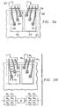
- FIG. 2B indicates schematically the electrical consequences for the operation of the power transistor caused by the remote location of the connecting members to the power supply.
- FIG. 2B shows the same bus arrangement over the distributed source and drain regions of a power transistor, again with the contact pads arrayed along the chip periphery.
- three resistors 210 are shown, called Rb; they are in parallel.
- the distributed lateral linear resistors 211, called Rm are in series and represent a significant resistance for the current I flowing through the buses, causing significant voltage drops and current de-biasing.
- Rs is the resistance in the transistor itself; it has to be added in series. Estimating series and parallel arrangements of the resistors as indicated by the insert of FIG. 2B for a typical transistor layout, reveals a de-biasing effect of 10 to 30 % of the power transistor efficiency. It is a key feature of the present invention to eliminate, or at least to minimize, this loss.
- active circuitry is meant the various electrical components that provide functionality to the IC.
- active circuitry specifically refers to the power bus metal layer of laterally organized power transistors.
- FIG. 3A the simplified top view of a portion of an IC chip 300 is shown, with the area of the active power transistor surrounded by the dashed line 301.
- Sheet-like metal is formed as wide-area bus 302 for connecting all source electrodes, and as bus 303 for connecting all drain electrodes.
- the plurality of contact pads 304 is positioned over the buses (structure of the contact pads and method of fabrication are described below). With this arrangement, significant silicon real estate can be saved compared to the arrangement in FIG. 2A. Dependent on the number and size of contact pads, between about 10 and > 40 % of the chip area can be saved.
- the connecting members to the "outside world” are bonding wires 306, connecting pads 304 to outside leadframes 307 and thus to the power supply.
- wire bonding allow the formation of reliable ball contacts, long wires and tightly controlled shape of the wire loop.
- Such advances can, for instance, be found in the computerized bonder 8020 by Kulicke & Soffa, Willow Grove, PA, U.S.A., or in the ABACUS SA by Texas Instruments, Dallas, TX, USA Moving the capillary in a predetermined and computer-controlled manner through the air will create a wire looping of exactly defined shape. For instance, with the recent technical advances, rounded, trapezoidal, linear and customized loop paths can be formed.
- FIG. 3B depicts schematically the electrical advantages for the operation of the power transistor caused by the over-the-transistor location of the connecting members to the power supply.
- the positioning of the bonding pads provides a regime of sheet resistance rather than the lateral linear resistor of FIG. 2B, thus enabling a reduction of about 30 to > 60 % of the resistance. Consequently, the voltage drop correlated with this resistance and thus the corresponding de-biasing effect are reduced, and the transistor performance improved.
- the spreading resistances Rm are now in series with the various wire resistances Rb, yet the resulting resistances are in parallel to each other, thus reducing the overall resistance.
- Rs the resistance in the transistor itself, remains unchanged compare to the inset diagram in FIG. 2B.
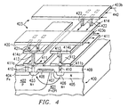
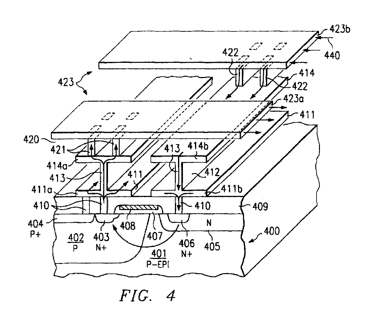
- FIG. 4 combines a simplified cross section of an integrated lateral power transistor with a perspective view of the power supply to this transistor.
- Lateral DMOS transistor 400 is fabricated in p-epitaxial layer 401.
- Lateral DMOS transistor 400 includes a DWELL region 402, n+ source region 403, p+ back gate region 404, RESURF region 405, n+ drain region 406, gate oxide 407, and polysilicon gate 408.
- Lateral DMOS transistor 400 could be manufactured using the lateral DMOS process described in U.S. Patent Serial Number 5,272,098, which is hereby incorporated by reference.
- lateral DMOS transistor 400 could be manufactured according to the methods described in U.S. Patent No. 5,242,841 or U.S. Patent No. 5,306,652, which are hereby incorporated by reference.
- an interlevel insulator layer 409 is deposited. Insulator layer 409 is then patterned and etched to form vias 410, using standard photolithographic techniques.
- Metallization layer 411 is deposited over insulator layer 409 and into vias 410 and patterned and etched. Metal layer 411 is sometimes referred to as "metal 1".
- the patterned portion 411a which is in contact with source region 403, serves as source electrode of the transistor, and the patterned portion 411b, which is in contact with drain region 406, serves as drain electrode.
- a second interlevel insulator layer 412 (indicated in FIG.
- metallization layer 414 is deposited over insulator layer 412 and into vias 413 and patterned and etched.
- Metal layer 414 is sometimes referred to as "metal 2".
- the patterned portion 414a which is in contact with layer portion 411a, serves as an extension of the source electrode of the transistor.
- the patterned portion 414b which is in contact with layer portion 411b, serves as an extension of the drain electrode of the transistor.
- Insulator layers 409 and 412 may be formed from a nitride, oxide, nitride/oxide combination, SOG, BPSG, or low-k gel, for example.
- metallization layers 411 and 414 are aluminum, although other metals such as copper or metal alloys could also be used. Although two metallization layers 411 and 414 are shown in FIG. 4, it is understood that a single metallization layer or more than two metallization layers could be used.
- Overcoat layer 420 (indicated in FIG. 4 as an open space) is deposited on the surface of the semiconductor wafer, uniformly covering the metallization layers 414.
- Overcoat layer 420 may be made from standard electrically non-conductive material, or it may be moisture impenetrable and able to protect metallization layer 414 during subsequent fabrication. Examples of suitable materials are silicon nitride, silicon oxynitride, silicon carbon alloys, oxide/nitride combinations, polyimide, and sandwiched films thereof. The thickness may range from about 400 to 1500 ⁇ m.
- vias 421 and 422 are formed through the overcoat layer 420 to metallization layer 414.
- the plurality of vias 421 is intended to open to the source metallization of the transistor, while the plurality of vias 422 is intended to open to the drain metallization of the transistor.
- Metallization layer 423 is deposited over insulator layer 420 and into vias 421 and 422 and patterned and etched. Metal layer 423 is sometimes referred to as "metal 3".
- the patterned portion 423a which is in contact with vias 421 and layer portions 414a and 411a, serves as bus for the source electrodes of the transistor.
- the patterned portion 423b which is in contact with vias 422 and layer portions 414b and 411b, serves as bus for the drain electrodes of the transistor.
- FIG. 5 is a continuation upwards from layers 423a and 423b shown in FIG. 5, illustrating the continued fabrication process flow.
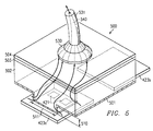
- FIG. 5 combines a simplified cross section of the top portion of a power transistor with a perspective view of a contact pad generally designated 500.
- Contact pad 500 could be manufactured using the process described in U.S. Patent Application Serial Number 09/611,623 entitled “Integrated Circuit With Bonding Layer Over Active Circuitry", filed 7 July 2000, which is hereby incorporated by reference.
- contact pad 500 is serving specifically the source bus 423a; analogous consideration holds for the contact pads serving the drain bus 423b.
- a mechanically strong, electrically insulating film 510 (indicated in FIG. 5 as an open space) is deposited over the complete wafer surface including the bus metallizations. Similar to overcoat layer 420, the material is selected from a group consisting of silicon nitride, silicon oxynitride, silicon carbon alloys, polyimide, and sandwiched films thereof. The thickness ranges from about 400 to 1500 nm.
- opening 511 is formed in insulating film 510. It is important for the present invention that opening 511 is positioned vertically over at least one of the vias 421 or 422. In the example of FIG. 5, the opening is positioned vertically over at least one via 421 connecting the source bus to one of the source metallizations. In an analogous case, the opening may be positioned vertically over at least one of the vias 422 connecting the drain bus to one of the drain metallizations.
- the opening 511 is filled with metal of the layers forming stack 500.
- Contact pad 500 consists of a seed metal layer 501, a first stress-absorbing metal layer 502, a second stress absorbing layer 503 and an outermost bondable metal layer 504.
- Seed metal layer 501 is selected from a group consisting of tungsten, titanium, titanium nitride, molybdenum, chromium, and alloys thereof.
- the seed metal layer is electrically conductive, provides adhesion to both the bus metal and the protective overcoat, permits the exposed portions of its upper surface to be electroplated, and prevents migration of the subsequent stress-absorbing metals to the bus metallization layers.
- the thickness of seed metal layer 501 is between about 100 and 500 nm.
- the seed metal layer 501 may be composed of two metal layers; an example for the second metal is copper, since it provides a suitable surface for subsequent electroplating.
- a single seed layer can preferably be made of refractory metal which has a thickness large enough to reliably act as a stress-absorbing buffer. Thicknesses between about 200 and 500 nm, preferably about 300 nm, are satisfactory. The thickness for optimum stress absorption depends not only on the selected metal, but also on the deposition technique selected, the rate of deposition, and the temperature of the silicon substrate during the time of deposition, since these parameters determine the microcrystallinity of the deposited layer.
- the layer formation is preferably performed at a rate of about 4 to 5 nm/s onto a silicon substrate at ambient temperature, increasing to about 70 °C when a thickness of at least 300 nm is reached.
- the tungsten microcrystals thus created have an average size and distribution such that they act reliably as stress-absorbing "springs" during the wire bonding process in assembly.
- first stress-absorbing metal layer 502 is copper. Its thickness in the range from about 2 to 35 ⁇ m makes it a mechanically strong support layer for subsequent attachment of connecting members such as bonding wires.
- second stress-absorbing metal layer 503 is nickel in the thickness range from bout 1 to 5 ⁇ m.
- the outermost layer 504 is metallurgically bondable or solderable. If wire bonding is the connecting method selected and layer 504 should be bondable, favorable metal choices include pure or alloyed aluminum, gold palladium, and silver. If soldering is the connecting method selected and layer 504 should be solderable, favorable metal choices include palladium, gold, silver and platinum. In both cases, the thickness is in the 500 to 2800 nm range. It is understood that the number of layers, the choice of materials and their thicknesses, and the deposition processes can be varied in order to suit specific device needs.
- the plating pattern of the contact pads may form any desired pattern.
- the connector stack 500 has its opening to the source bus located vertically over the vias to the source metallization, yet it extends geometrically beyond the direct area of the opening.
- the contact pad 500 extend over the adjacent drain bus 423b, from which it is isolated by dielectric layer 510.
- This arrangement provides for sufficient surface area of the pad to attach the ball 530 (even relatively large ones) of a bonding wire 531.
- Contact pad 500 is equally well suited for attaching a wedge bond or a stitch bond.
- the other end of wire 531 may be bonded to a leadframe (see FIGs. 2 and 3) or substrate carrying a conductive pattern on which the IC chip is mounted.
- outermost layer 504 may be selected so that it is solderable. A solder ball can then be attached to it by standard reflow techniques.
- an additional solder mask or polyimide layer (not shown in FIG. 5) with an opening for each solder ball in order to keep the flip-chip bump in a defined area and shape during bump formation and subsequent attachment to an external package or board.
- FIG. 4 in combination with FIG. 5 highlights the pivotal feature of the present invention how the placement of bonds over the active power transistor enables short-distance vertical current flow and minimizes long-distance lateral current flow. In other words, electrical resistance in current flow is minimized.
- electrical current 440 from the drain bond flows, in conventional directional nomenclature, through drain bus 423b to the vias 422. Flowing vertically through vias 422 into drain electrodes 414b, and vertically through vias 413 and 410, the current flows into the drain of the power transistor. After exiting the power transistor as source current, it flows again vertically through vias 410 and 413 to the source electrode 414a. Continuing vertically through vias 421 into the source bus 423a, the current enters through opening 511 into the contact pad 500 and continues vertically into bond wire 531. The current 540 flows to the source bond.
- a semiconductor integrated circuit comprising: contact pads located over active components; and the position of said pads selected to provide control and distribution of power to said active components below said pads.
- the contact pad positions may further be selected to provide dissipation of thermal energy released by said active components.
- a semiconductor integrated circuit comprising: contact pads located over active components; and said pads positioned to minimize the distance for power delivery between a selected pad and one or more corresponding active components, to which said power is to be delivered. The minimum distance further may be selected to maximize dissipation of thermal energy released by said active components.
- a semiconductor integrated circuit comprising: a laterally organized power transistor; an array of power supply contact pads distributed over said power transistor; means for providing a distributed, predominantly vertical current flow from said contact pads to said transistor; and means for connecting a power source to each of said contact pads.
- the invention covers generally a semiconductor integrated circuit which comprises contact pads located over active components, and the position of these pads are selected so that they provide control and distribution of power to the active components below the pads.
- the invention covers a semiconductor IC which comprises contact pads located over active components, and these pads are positioned to minimize the distance for power delivery between a selected pad and one or more corresponding active components, to which the power is to be delivered.
Landscapes
- Internal Circuitry In Semiconductor Integrated Circuit Devices (AREA)
- Wire Bonding (AREA)
- Semiconductor Integrated Circuits (AREA)
- Metal-Oxide And Bipolar Metal-Oxide Semiconductor Integrated Circuits (AREA)
- Design And Manufacture Of Integrated Circuits (AREA)
- Insulated Gate Type Field-Effect Transistor (AREA)
- Electrodes Of Semiconductors (AREA)
Abstract
Description
Claims (24)
- A semiconductor device comprising:a semiconductor substrate;an active circuit fabricated on said substrate and comprised of an integrated power transistor, said circuit having at least one metallization layer forming a plurality of first and second electrodes of said transistor;a first bus connecting all of said first electrodes, and a second bus connecting all of said second electrodes, each bus connected to said respective electrode by metal-filled vias, whereby said buses are positioned directly over said transistor;a mechanically strong, electrically insulating film overlaying said circuit, said transistor, and said buses;a plurality of contact pads distributed over each of said buses, each of said pads having a stack of stress-absorbing metal layers, the outermost layer being metallurgically attachable, and a connection to the underlying bus through openings in said insulating film, said openings positioned substantially vertically over at least one of said vias; andat least one connecting member attached to said contact pads, whereby the electrical current path and resistance from said member to said electrodes are minimized, improving the electrical characteristics of said power transistor.
- The device according to Claim 1, wherein said substrate is selected from a group consisting of silicon, silicon germanium, gallium arsenide, and any other semiconductor material customarily used in electronic device production.
- The device according to Claim 1 or Claim 2, wherein said circuit comprises a plurality of active and passive electronic components arranged horizontally and vertically.
- The device according to any of Claims 1 to 3, wherein said power transistor is laid out horizontally, having said electrodes arranged in a plurality of metal bands substantially parallel to each other.
- The device according to Claim 4, wherein said power transistor comprises electrical current flowing horizontally through said electrodes and said semiconductor between said electrodes.
- The device according to any of Claims 1 to 5, wherein said at least one metallization layer is made of pure or alloyed copper, aluminum, nickel, or refractory metals.
- The device according to any of Claims 1 to 6, wherein said electrically insulating film further serves as the protective overcoat of said integrated circuit.
- The device according to any of Claims 1 to 7, wherein said electrically insulating film comprises materials selected from a group consisting of silicon nitride, silicon oxynitride, silicon carbon alloys, polyimide and sandwiched films thereof.
- The device according to Claim 8, wherein said electrically insulating film is between about 400 and 1500 nm thick.
- The device according to any of Claims 1 to 9, wherein said stack of metal layers of said contact pads comprise a layer of seed metal on said bus bar, promoting adhesion to said bus bars and inhibiting migration of overlying metals to said bus bar, at least one stress-absorbing metal layer, and an outermost metallurgically attachable metal layer.
- The device according to Claim 10, wherein said seed metal layer is selected from a group consisting of tungsten, titanium, titanium nitride, molybdenum, chromium, and alloys thereof.
- The device according to Claim 11, wherein said layer of seed metal is between about 200 and 500 nm thick.
- The device according to any of Claims 10 to 12, wherein said stress-absorbing metal layer comprises at least one layer selected from a group consisting of copper, nickel, aluminum, and alloys thereof.
- The device according to Claim 13, wherein said stress-absorbing metal layer is between about 2 and 35 µm thick.
- The device according to any of Claims 10 to 14, wherein said outermost metal layer is metallurgically bondable or solderable.
- The device according to Claim 15, wherein said outermost bondable metal layer is selected from a group consisting of pure or alloyed aluminum, gold, palladium, and silver.
- The device according to Claim 15 or Claim 16, wherein said solderable metal layer is selected from a group consisting of palladium, gold, silver and platinum.
- The device according to any of Claims 15 to 17, wherein said outermost layer is between about 500 and 2800 nm thick.
- The device according to any of Claims 1 to 18, wherein said connecting member is a bonding wire or a solder ball.
- The device according to Claim 19, wherein said bonding wire is selected from a group consisting of pure or alloyed gold, copper, and aluminum.
- The device according to Claim 19 or Claim 20, wherein said solder ball is selected from a group consisting of tin, tin alloys including tin/copper, tin/indium, tin/silver, tin/bismuth, tin/lead, and conductive adhesive compounds.
- A method for fabricating an active circuit on a semiconductor substrate, said circuit having an integrated power transistor and at least one metallization layer forming a plurality of first and second electrodes of said transistor, which method comprising:forming a first bus connecting all of said first electrodes and a second bus connecting all of said second electrodes, each bus connected to said respective electrode by metal-filled vias, thereby positioning said buses directly over said transistor;depositing a mechanically strong, electrically insulating film over said circuit, said transistor and said buses;forming a plurality of openings through said film to said buses, each of said openings positioned substantially vertically over at least one of said vias;filling said openings by depositing a stack of stress-absorbing metal layers on said film, the outermost layer being metallurgically attachable;forming a plurality of contact pads from said stack of layers, each pad comprising at least one of said openings;attaching at least one connecting member to said contact pads, thereby creating an electrical current path from said member to said electrodes of minimum length and minimum resistance, thus improving the electrical characteristics of said power transistor.
- The method according to Claim 22, wherein said step of depositing said stack of metal layers comprises:depositing a seed metal layer on the surface of said substrate;forming a plating pattern over said seed metal layer, said plating pattern resulting in exposed portions of said seed metal layer and blocking the rest of said seed metal layer;covering said exposed portions of said seed metal layer with an electrically conductive, stress-absorbing support layer;covering said support layer with a metallurgically attachable layer; andremoving said blocked portions of said seed metal layer.
- The method according to Claim 22 or Claim 23, wherein said step of attaching of a connecting member comprises either bonding a wire to said contact pad, or reflowing a solder ball to said pad.
Applications Claiming Priority (2)
| Application Number | Priority Date | Filing Date | Title |
|---|---|---|---|
| US22105100P | 2000-07-27 | 2000-07-27 | |
| US221051P | 2000-07-27 |
Publications (3)
| Publication Number | Publication Date |
|---|---|
| EP1176640A2 true EP1176640A2 (en) | 2002-01-30 |
| EP1176640A3 EP1176640A3 (en) | 2004-03-17 |
| EP1176640B1 EP1176640B1 (en) | 2008-02-20 |
Family
ID=22826133
Family Applications (1)
| Application Number | Title | Priority Date | Filing Date |
|---|---|---|---|
| EP01000318A Expired - Lifetime EP1176640B1 (en) | 2000-07-27 | 2001-07-27 | Contact structure of an integrated power circuit |
Country Status (5)
| Country | Link |
|---|---|
| US (1) | US7045903B2 (en) |
| EP (1) | EP1176640B1 (en) |
| JP (1) | JP2002164437A (en) |
| AT (1) | ATE387012T1 (en) |
| DE (1) | DE60132855T2 (en) |
Cited By (3)
| Publication number | Priority date | Publication date | Assignee | Title |
|---|---|---|---|---|
| WO2003058716A1 (en) * | 2002-01-12 | 2003-07-17 | Philips Intellectual Property & Standards Gmbh | Discrete semiconductor component |
| US8994145B2 (en) | 2010-12-27 | 2015-03-31 | Kabushiki Kaisha Toshiba | Semiconductor device including capacitor under pad |
| WO2019139705A1 (en) * | 2018-01-10 | 2019-07-18 | Qualcomm Incorporated | POWER DISTRIBUTION NETWORKS (PDNs) USING HYBRID GRID AND PILLAR ARRANGEMENTS |
Families Citing this family (39)
| Publication number | Priority date | Publication date | Assignee | Title |
|---|---|---|---|---|
| US6104761A (en) | 1998-08-28 | 2000-08-15 | Sicom, Inc. | Constrained-envelope digital-communications transmission system and method therefor |
| US6972464B2 (en) * | 2002-10-08 | 2005-12-06 | Great Wall Semiconductor Corporation | Power MOSFET |
| JP4396200B2 (en) * | 2002-10-30 | 2010-01-13 | 株式会社デンソー | Semiconductor device |
| JP2004303861A (en) * | 2003-03-31 | 2004-10-28 | Renesas Technology Corp | Semiconductor device and method of manufacturing the same |
| US8274160B2 (en) | 2003-08-21 | 2012-09-25 | Intersil Americas Inc. | Active area bonding compatible high current structures |
| US7005369B2 (en) * | 2003-08-21 | 2006-02-28 | Intersil American Inc. | Active area bonding compatible high current structures |
| US7495296B2 (en) * | 2004-06-01 | 2009-02-24 | Panasonic Corporation | Semiconductor integrated circuit device |
| KR100615579B1 (en) | 2004-09-20 | 2006-08-25 | 삼성전자주식회사 | Semiconductor memory device and power line arrangement method thereof |
| KR100675275B1 (en) * | 2004-12-16 | 2007-01-26 | 삼성전자주식회사 | Semiconductor Device and Pad Arrangement Method |
| US7404513B2 (en) * | 2004-12-30 | 2008-07-29 | Texas Instruments Incorporated | Wire bonds having pressure-absorbing balls |
| US7476976B2 (en) * | 2005-02-23 | 2009-01-13 | Texas Instruments Incorporated | Flip chip package with advanced electrical and thermal properties for high current designs |
| US7483248B1 (en) * | 2005-05-19 | 2009-01-27 | Sun Microsystems, Inc. | Method and apparatus for detecting current changes in integrated circuits |
| KR100849640B1 (en) | 2005-09-16 | 2008-08-01 | 가부시키가이샤 리코 | Semiconductor devices |
| DE102006050087A1 (en) * | 2006-10-24 | 2008-04-30 | Austriamicrosystems Ag | Semiconductor body for use in diode and transistor such as FET and bi-polar transistor, has connecting line for contacting semiconductor region, where conductivity per unit of length of connecting line changes from value to another value |
| US7667316B2 (en) * | 2006-10-31 | 2010-02-23 | Panasonic Corporation | Semiconductor integrated circuit and method for manufacturing the same |
| JP5054359B2 (en) * | 2006-12-01 | 2012-10-24 | パナソニック株式会社 | Semiconductor integrated circuit and manufacturing method thereof |
| JP4814770B2 (en) * | 2006-12-01 | 2011-11-16 | パナソニック株式会社 | Semiconductor integrated circuit |
| JP5066928B2 (en) * | 2007-02-08 | 2012-11-07 | 株式会社デンソー | Semiconductor device |
| JP2008218442A (en) * | 2007-02-28 | 2008-09-18 | Matsushita Electric Ind Co Ltd | Semiconductor integrated circuit device and manufacturing method thereof |
| DE102007036566A1 (en) * | 2007-08-03 | 2009-02-19 | Siemens Ag | Spring contact of electrical contact surfaces of an electronic component |
| US7800239B2 (en) * | 2007-12-14 | 2010-09-21 | Semiconductor Components Industries, Llc | Thick metal interconnect with metal pad caps at selective sites and process for making the same |
| JP5326151B2 (en) * | 2007-12-26 | 2013-10-30 | セイコーNpc株式会社 | Power MOS transistor |
| DE102007063268A1 (en) * | 2007-12-31 | 2009-07-09 | Advanced Micro Devices, Inc., Sunnyvale | Wire bond with aluminum-free metallization layers through surface conditioning |
| US20100059795A1 (en) * | 2008-09-08 | 2010-03-11 | Firas Azrai | Vertical current transport in a power converter circuit |
| KR101107659B1 (en) * | 2010-02-05 | 2012-01-20 | 주식회사 하이닉스반도체 | Semiconductor package |
| US8240218B2 (en) * | 2010-03-01 | 2012-08-14 | Infineon Technologies Ag | Stress sensing devices and methods |
| US8426971B2 (en) | 2010-08-27 | 2013-04-23 | Diodes FabTech, Inc. | Top tri-metal system for silicon power semiconductor devices |
| JP5580230B2 (en) | 2011-02-28 | 2014-08-27 | パナソニック株式会社 | Semiconductor device |
| US9006099B2 (en) * | 2011-06-08 | 2015-04-14 | Great Wall Semiconductor Corporation | Semiconductor device and method of forming a power MOSFET with interconnect structure silicide layer and low profile bump |
| US9105552B2 (en) | 2011-10-31 | 2015-08-11 | Taiwan Semiconductor Manufacturing Company, Ltd. | Package on package devices and methods of packaging semiconductor dies |
| US8823180B2 (en) * | 2011-12-28 | 2014-09-02 | Taiwan Semiconductor Manufacturing Company, Ltd. | Package on package devices and methods of packaging semiconductor dies |
| US8859416B2 (en) * | 2012-04-24 | 2014-10-14 | GlobalFoundries, Inc. | Software and method for via spacing in a semiconductor device |
| US9171790B2 (en) | 2012-05-30 | 2015-10-27 | Taiwan Semiconductor Manufacturing Company, Ltd. | Package on package devices and methods of packaging semiconductor dies |
| WO2013179547A1 (en) * | 2012-06-01 | 2013-12-05 | パナソニック株式会社 | Power semiconductor device |
| TWI632644B (en) * | 2017-08-30 | 2018-08-11 | Airoha Technology Corp. | Integrated circuit structure |
| TWI748233B (en) * | 2018-08-29 | 2021-12-01 | 美商高效電源轉換公司 | Lateral power device with reduced on-resistance |
| JP7177660B2 (en) * | 2018-10-26 | 2022-11-24 | 株式会社東芝 | semiconductor equipment |
| WO2022130906A1 (en) | 2020-12-18 | 2022-06-23 | ローム株式会社 | Semiconductor equipment |
| US12159871B2 (en) | 2021-07-01 | 2024-12-03 | Innoscience (Suzhou) Technology Co., Ltd. | Nitride-based multi-channel switching semiconductor device and method for manufacturing the same |
Family Cites Families (7)
| Publication number | Priority date | Publication date | Assignee | Title |
|---|---|---|---|---|
| JPS5992537A (en) * | 1982-11-19 | 1984-05-28 | Hitachi Ltd | Semiconductor device |
| EP0646959B1 (en) * | 1993-09-30 | 2001-08-16 | Consorzio per la Ricerca sulla Microelettronica nel Mezzogiorno | Metallization and bonding process for manufacturing power semiconductor devices |
| US6150722A (en) * | 1994-11-02 | 2000-11-21 | Texas Instruments Incorporated | Ldmos transistor with thick copper interconnect |
| US5665996A (en) * | 1994-12-30 | 1997-09-09 | Siliconix Incorporated | Vertical power mosfet having thick metal layer to reduce distributed resistance |
| JPH08293523A (en) * | 1995-02-21 | 1996-11-05 | Seiko Epson Corp | Semiconductor device and manufacturing method thereof |
| JP2000183104A (en) * | 1998-12-15 | 2000-06-30 | Texas Instr Inc <Ti> | System and method for bonding on an integrated circuit |
| US6291331B1 (en) * | 1999-10-04 | 2001-09-18 | Taiwan Semiconductor Manufacturing Company | Re-deposition high compressive stress PECVD oxide film after IMD CMP process to solve more than 5 metal stack via process IMD crack issue |
-
2001
- 2001-07-27 JP JP2001262416A patent/JP2002164437A/en not_active Abandoned
- 2001-07-27 DE DE60132855T patent/DE60132855T2/en not_active Expired - Lifetime
- 2001-07-27 EP EP01000318A patent/EP1176640B1/en not_active Expired - Lifetime
- 2001-07-27 AT AT01000318T patent/ATE387012T1/en not_active IP Right Cessation
- 2001-07-30 US US09/917,419 patent/US7045903B2/en not_active Expired - Lifetime
Cited By (6)
| Publication number | Priority date | Publication date | Assignee | Title |
|---|---|---|---|---|
| WO2003058716A1 (en) * | 2002-01-12 | 2003-07-17 | Philips Intellectual Property & Standards Gmbh | Discrete semiconductor component |
| US8994145B2 (en) | 2010-12-27 | 2015-03-31 | Kabushiki Kaisha Toshiba | Semiconductor device including capacitor under pad |
| WO2019139705A1 (en) * | 2018-01-10 | 2019-07-18 | Qualcomm Incorporated | POWER DISTRIBUTION NETWORKS (PDNs) USING HYBRID GRID AND PILLAR ARRANGEMENTS |
| US10380308B2 (en) | 2018-01-10 | 2019-08-13 | Qualcomm Incorporated | Power distribution networks (PDNs) using hybrid grid and pillar arrangements |
| CN111602243A (en) * | 2018-01-10 | 2020-08-28 | 高通股份有限公司 | Power Distribution Network (PDN) using hybrid grid and post arrangements |
| CN111602243B (en) * | 2018-01-10 | 2024-06-11 | 高通股份有限公司 | Power distribution network (PDN) using hybrid grid and pillar arrangements |
Also Published As
| Publication number | Publication date |
|---|---|
| ATE387012T1 (en) | 2008-03-15 |
| JP2002164437A (en) | 2002-06-07 |
| EP1176640B1 (en) | 2008-02-20 |
| US20020011674A1 (en) | 2002-01-31 |
| DE60132855T2 (en) | 2009-02-26 |
| DE60132855D1 (en) | 2008-04-03 |
| US7045903B2 (en) | 2006-05-16 |
| EP1176640A3 (en) | 2004-03-17 |
Similar Documents
| Publication | Publication Date | Title |
|---|---|---|
| EP1176640B1 (en) | Contact structure of an integrated power circuit | |
| US7514292B2 (en) | Individualized low parasitic power distribution lines deposited over active integrated circuits | |
| US6384486B2 (en) | Bonding over integrated circuits | |
| US6683380B2 (en) | Integrated circuit with bonding layer over active circuitry | |
| US6544880B1 (en) | Method of improving copper interconnects of semiconductor devices for bonding | |
| CN101202266B (en) | Chip-scale packaging, manufacturing method thereof, and high-power integrated circuit device | |
| US9153555B2 (en) | Method of wire bonding over active area of a semiconductor circuit | |
| US8329508B2 (en) | Semiconductor die packages using thin dies and metal substrates | |
| US7060607B2 (en) | Circuit method integrating the power distribution functions of the circuits and leadframes into the chip surface | |
| US7425767B2 (en) | Chip structure with redistribution traces | |
| US20070187823A1 (en) | Semiconductor device | |
| US6784539B2 (en) | Thermally enhanced semiconductor chip having integrated bonds over active circuits | |
| CN223638364U (en) | Conductive bump structure |
Legal Events
| Date | Code | Title | Description |
|---|---|---|---|
| PUAI | Public reference made under article 153(3) epc to a published international application that has entered the european phase |
Free format text: ORIGINAL CODE: 0009012 |
|
| AK | Designated contracting states |
Kind code of ref document: A2 Designated state(s): AT BE CH CY DE DK ES FI FR GB GR IE IT LI LU MC NL PT SE TR |
|
| AX | Request for extension of the european patent |
Free format text: AL;LT;LV;MK;RO;SI |
|
| PUAL | Search report despatched |
Free format text: ORIGINAL CODE: 0009013 |
|
| AK | Designated contracting states |
Kind code of ref document: A3 Designated state(s): AT BE CH CY DE DK ES FI FR GB GR IE IT LI LU MC NL PT SE TR |
|
| AX | Request for extension of the european patent |
Extension state: AL LT LV MK RO SI |
|
| RIC1 | Information provided on ipc code assigned before grant |
Ipc: 7H 01L 23/485 A Ipc: 7H 01L 23/528 B |
|
| 17P | Request for examination filed |
Effective date: 20040917 |
|
| AKX | Designation fees paid |
Designated state(s): AT BE CH CY DE DK ES FI FR GB GR IE IT LI LU MC NL PT SE TR |
|
| GRAP | Despatch of communication of intention to grant a patent |
Free format text: ORIGINAL CODE: EPIDOSNIGR1 |
|
| GRAS | Grant fee paid |
Free format text: ORIGINAL CODE: EPIDOSNIGR3 |
|
| GRAA | (expected) grant |
Free format text: ORIGINAL CODE: 0009210 |
|
| AK | Designated contracting states |
Kind code of ref document: B1 Designated state(s): AT BE CH CY DE DK ES FI FR GB GR IE IT LI LU MC NL PT SE TR |
|
| REG | Reference to a national code |
Ref country code: GB Ref legal event code: FG4D |
|
| REG | Reference to a national code |
Ref country code: CH Ref legal event code: EP |
|
| REG | Reference to a national code |
Ref country code: IE Ref legal event code: FG4D |
|
| REF | Corresponds to: |
Ref document number: 60132855 Country of ref document: DE Date of ref document: 20080403 Kind code of ref document: P |
|
| PG25 | Lapsed in a contracting state [announced via postgrant information from national office to epo] |
Ref country code: FI Free format text: LAPSE BECAUSE OF FAILURE TO SUBMIT A TRANSLATION OF THE DESCRIPTION OR TO PAY THE FEE WITHIN THE PRESCRIBED TIME-LIMIT Effective date: 20080220 Ref country code: ES Free format text: LAPSE BECAUSE OF FAILURE TO SUBMIT A TRANSLATION OF THE DESCRIPTION OR TO PAY THE FEE WITHIN THE PRESCRIBED TIME-LIMIT Effective date: 20080531 |
|
| NLV1 | Nl: lapsed or annulled due to failure to fulfill the requirements of art. 29p and 29m of the patents act | ||
| ET | Fr: translation filed | ||
| PG25 | Lapsed in a contracting state [announced via postgrant information from national office to epo] |
Ref country code: AT Free format text: LAPSE BECAUSE OF FAILURE TO SUBMIT A TRANSLATION OF THE DESCRIPTION OR TO PAY THE FEE WITHIN THE PRESCRIBED TIME-LIMIT Effective date: 20080220 |
|
| PG25 | Lapsed in a contracting state [announced via postgrant information from national office to epo] |
Ref country code: BE Free format text: LAPSE BECAUSE OF FAILURE TO SUBMIT A TRANSLATION OF THE DESCRIPTION OR TO PAY THE FEE WITHIN THE PRESCRIBED TIME-LIMIT Effective date: 20080220 |
|
| PG25 | Lapsed in a contracting state [announced via postgrant information from national office to epo] |
Ref country code: DK Free format text: LAPSE BECAUSE OF FAILURE TO SUBMIT A TRANSLATION OF THE DESCRIPTION OR TO PAY THE FEE WITHIN THE PRESCRIBED TIME-LIMIT Effective date: 20080220 Ref country code: NL Free format text: LAPSE BECAUSE OF FAILURE TO SUBMIT A TRANSLATION OF THE DESCRIPTION OR TO PAY THE FEE WITHIN THE PRESCRIBED TIME-LIMIT Effective date: 20080220 Ref country code: PT Free format text: LAPSE BECAUSE OF FAILURE TO SUBMIT A TRANSLATION OF THE DESCRIPTION OR TO PAY THE FEE WITHIN THE PRESCRIBED TIME-LIMIT Effective date: 20080721 Ref country code: SE Free format text: LAPSE BECAUSE OF FAILURE TO SUBMIT A TRANSLATION OF THE DESCRIPTION OR TO PAY THE FEE WITHIN THE PRESCRIBED TIME-LIMIT Effective date: 20080520 |
|
| PLBE | No opposition filed within time limit |
Free format text: ORIGINAL CODE: 0009261 |
|
| STAA | Information on the status of an ep patent application or granted ep patent |
Free format text: STATUS: NO OPPOSITION FILED WITHIN TIME LIMIT |
|
| 26N | No opposition filed |
Effective date: 20081121 |
|
| REG | Reference to a national code |
Ref country code: CH Ref legal event code: PL |
|
| PG25 | Lapsed in a contracting state [announced via postgrant information from national office to epo] |
Ref country code: MC Free format text: LAPSE BECAUSE OF NON-PAYMENT OF DUE FEES Effective date: 20080731 |
|
| PG25 | Lapsed in a contracting state [announced via postgrant information from national office to epo] |
Ref country code: CH Free format text: LAPSE BECAUSE OF NON-PAYMENT OF DUE FEES Effective date: 20080731 Ref country code: LI Free format text: LAPSE BECAUSE OF NON-PAYMENT OF DUE FEES Effective date: 20080731 |
|
| PG25 | Lapsed in a contracting state [announced via postgrant information from national office to epo] |
Ref country code: IE Free format text: LAPSE BECAUSE OF NON-PAYMENT OF DUE FEES Effective date: 20080728 Ref country code: CY Free format text: LAPSE BECAUSE OF FAILURE TO SUBMIT A TRANSLATION OF THE DESCRIPTION OR TO PAY THE FEE WITHIN THE PRESCRIBED TIME-LIMIT Effective date: 20080220 |
|
| PG25 | Lapsed in a contracting state [announced via postgrant information from national office to epo] |
Ref country code: IT Free format text: LAPSE BECAUSE OF FAILURE TO SUBMIT A TRANSLATION OF THE DESCRIPTION OR TO PAY THE FEE WITHIN THE PRESCRIBED TIME-LIMIT Effective date: 20080220 |
|
| PG25 | Lapsed in a contracting state [announced via postgrant information from national office to epo] |
Ref country code: LU Free format text: LAPSE BECAUSE OF NON-PAYMENT OF DUE FEES Effective date: 20080727 |
|
| PG25 | Lapsed in a contracting state [announced via postgrant information from national office to epo] |
Ref country code: TR Free format text: LAPSE BECAUSE OF FAILURE TO SUBMIT A TRANSLATION OF THE DESCRIPTION OR TO PAY THE FEE WITHIN THE PRESCRIBED TIME-LIMIT Effective date: 20080220 |
|
| PG25 | Lapsed in a contracting state [announced via postgrant information from national office to epo] |
Ref country code: GR Free format text: LAPSE BECAUSE OF FAILURE TO SUBMIT A TRANSLATION OF THE DESCRIPTION OR TO PAY THE FEE WITHIN THE PRESCRIBED TIME-LIMIT Effective date: 20080521 |
|
| REG | Reference to a national code |
Ref country code: FR Ref legal event code: PLFP Year of fee payment: 16 |
|
| REG | Reference to a national code |
Ref country code: FR Ref legal event code: PLFP Year of fee payment: 17 |
|
| REG | Reference to a national code |
Ref country code: FR Ref legal event code: PLFP Year of fee payment: 18 |
|
| PGFP | Annual fee paid to national office [announced via postgrant information from national office to epo] |
Ref country code: FR Payment date: 20200623 Year of fee payment: 20 |
|
| PGFP | Annual fee paid to national office [announced via postgrant information from national office to epo] |
Ref country code: GB Payment date: 20200624 Year of fee payment: 20 |
|
| PGFP | Annual fee paid to national office [announced via postgrant information from national office to epo] |
Ref country code: DE Payment date: 20200622 Year of fee payment: 20 |
|
| REG | Reference to a national code |
Ref country code: DE Ref legal event code: R071 Ref document number: 60132855 Country of ref document: DE |
|
| REG | Reference to a national code |
Ref country code: GB Ref legal event code: PE20 Expiry date: 20210726 |
|
| PG25 | Lapsed in a contracting state [announced via postgrant information from national office to epo] |
Ref country code: GB Free format text: LAPSE BECAUSE OF EXPIRATION OF PROTECTION Effective date: 20210726 |