EP1176425A1 - Current detecting apparatus and its control method - Google Patents
Current detecting apparatus and its control method Download PDFInfo
- Publication number
- EP1176425A1 EP1176425A1 EP01401987A EP01401987A EP1176425A1 EP 1176425 A1 EP1176425 A1 EP 1176425A1 EP 01401987 A EP01401987 A EP 01401987A EP 01401987 A EP01401987 A EP 01401987A EP 1176425 A1 EP1176425 A1 EP 1176425A1
- Authority
- EP
- European Patent Office
- Prior art keywords
- current
- resistor
- detecting
- transistor
- circuit
- Prior art date
- Legal status (The legal status is an assumption and is not a legal conclusion. Google has not performed a legal analysis and makes no representation as to the accuracy of the status listed.)
- Withdrawn
Links
Images








Classifications
-
- G—PHYSICS
- G01—MEASURING; TESTING
- G01R—MEASURING ELECTRIC VARIABLES; MEASURING MAGNETIC VARIABLES
- G01R19/00—Arrangements for measuring currents or voltages or for indicating presence or sign thereof
-
- G—PHYSICS
- G01—MEASURING; TESTING
- G01R—MEASURING ELECTRIC VARIABLES; MEASURING MAGNETIC VARIABLES
- G01R19/00—Arrangements for measuring currents or voltages or for indicating presence or sign thereof
- G01R19/0092—Measuring current only
-
- G—PHYSICS
- G01—MEASURING; TESTING
- G01R—MEASURING ELECTRIC VARIABLES; MEASURING MAGNETIC VARIABLES
- G01R15/00—Details of measuring arrangements of the types provided for in groups G01R17/00 - G01R29/00, G01R33/00 - G01R33/26 or G01R35/00
- G01R15/08—Circuits for altering the measuring range
- G01R15/09—Autoranging circuits
-
- H—ELECTRICITY
- H02—GENERATION; CONVERSION OR DISTRIBUTION OF ELECTRIC POWER
- H02J—ELECTRIC POWER NETWORKS; CIRCUIT ARRANGEMENTS OR SYSTEMS FOR SUPPLYING OR DISTRIBUTING ELECTRIC POWER; SYSTEMS FOR STORING ELECTRIC ENERGY
- H02J7/00—Circuit arrangements for charging or discharging batteries or for supplying loads from batteries
- H02J7/02—Circuit arrangements for charging or discharging batteries or for supplying loads from batteries for charging batteries from AC mains by converters
- H02J7/04—Regulation of charging current or voltage
-
- H—ELECTRICITY
- H02—GENERATION; CONVERSION OR DISTRIBUTION OF ELECTRIC POWER
- H02J—ELECTRIC POWER NETWORKS; CIRCUIT ARRANGEMENTS OR SYSTEMS FOR SUPPLYING OR DISTRIBUTING ELECTRIC POWER; SYSTEMS FOR STORING ELECTRIC ENERGY
- H02J7/00—Circuit arrangements for charging or discharging batteries or for supplying loads from batteries
- H02J7/90—Regulation of charging or discharging current or voltage
- H02J7/94—Regulation of charging or discharging current or voltage in response to battery current
- H02J7/953—Regulation of charging or discharging current or voltage in response to battery current in response to charge current gradient
-
- H—ELECTRICITY
- H02—GENERATION; CONVERSION OR DISTRIBUTION OF ELECTRIC POWER
- H02M—APPARATUS FOR CONVERSION BETWEEN AC AND AC, BETWEEN AC AND DC, OR BETWEEN DC AND DC, AND FOR USE WITH MAINS OR SIMILAR POWER SUPPLY SYSTEMS; CONVERSION OF DC OR AC INPUT POWER INTO SURGE OUTPUT POWER; CONTROL OR REGULATION THEREOF
- H02M3/00—Conversion of DC power input into DC power output
- H02M3/22—Conversion of DC power input into DC power output with intermediate conversion into AC
- H02M3/24—Conversion of DC power input into DC power output with intermediate conversion into AC by static converters
- H02M3/28—Conversion of DC power input into DC power output with intermediate conversion into AC by static converters using discharge tubes with control electrode or semiconductor devices with control electrode to produce the intermediate AC
- H02M3/325—Conversion of DC power input into DC power output with intermediate conversion into AC by static converters using discharge tubes with control electrode or semiconductor devices with control electrode to produce the intermediate AC using devices of a triode or a transistor type requiring continuous application of a control signal
- H02M3/335—Conversion of DC power input into DC power output with intermediate conversion into AC by static converters using discharge tubes with control electrode or semiconductor devices with control electrode to produce the intermediate AC using devices of a triode or a transistor type requiring continuous application of a control signal using semiconductor devices only
- H02M3/33507—Conversion of DC power input into DC power output with intermediate conversion into AC by static converters using discharge tubes with control electrode or semiconductor devices with control electrode to produce the intermediate AC using devices of a triode or a transistor type requiring continuous application of a control signal using semiconductor devices only with automatic control of the output voltage or current, e.g. flyback converters
- H02M3/33523—Conversion of DC power input into DC power output with intermediate conversion into AC by static converters using discharge tubes with control electrode or semiconductor devices with control electrode to produce the intermediate AC using devices of a triode or a transistor type requiring continuous application of a control signal using semiconductor devices only with automatic control of the output voltage or current, e.g. flyback converters with galvanic isolation between input and output of both the power stage and the feedback loop
-
- H—ELECTRICITY
- H02—GENERATION; CONVERSION OR DISTRIBUTION OF ELECTRIC POWER
- H02M—APPARATUS FOR CONVERSION BETWEEN AC AND AC, BETWEEN AC AND DC, OR BETWEEN DC AND DC, AND FOR USE WITH MAINS OR SIMILAR POWER SUPPLY SYSTEMS; CONVERSION OF DC OR AC INPUT POWER INTO SURGE OUTPUT POWER; CONTROL OR REGULATION THEREOF
- H02M1/00—Details of apparatus for conversion
- H02M1/0003—Details of control, feedback or regulation circuits
- H02M1/0009—Devices or circuits for detecting current in a converter
Definitions
- the invention relates to a current detecting apparatus which can precisely detect a current in a range from a small current to a large current and to a control method for such an apparatus.
- JP-A-10-28338 As a method of detecting a current, an example of detecting a current by using two power sources having a potential difference has been disclosed in JP-A-10-28338 by the same applicant of the present invention. According to JP-A-10-28338, it is intended to detect a value of a current at the time of charging a secondary battery.
- a voltage E1 of a power source 201 and a voltage E2 of a power source 203 are set so that a potential difference is equal to ⁇ V.
- the power source 201 can output a low voltage and a large current and the power source 203 can output a high voltage and a small current.
- a current is detected from a voltage across a resistor 202 having a small resistance value.
- a current is detected from a voltage across a resistor 204 having a large resistance value.
- an object of the invention to provide a current detecting apparatus in which since a detecting range of a current can be enlarged and the current can be independently detected, its influence can be minimized, errors can be reduced, and the loss can be decreased and to provide a control method of such an apparatus.
- a current detecting apparatus comprising: a first resistor provided between an input terminal and an output terminal; first switching means provided in parallel with the first resistor; control means for controlling the switching means: first detecting means for detecting a current flowing in the first resistor or a potential difference which is caused in the first resistor; a second resistor provided so as to be serial to at least the first switching means; and second detecting means for detecting a current flowing in the second resistor or a potential difference which is caused in the second resistor, wherein the control means turns off the switching means when the current or potential difference that is equal to or larger than a first predetermined value is detected by the first detecting means and turns on the switching means when the current or potential difference that is equal to or smaller than a second predetermined value is detected by the second detecting means, and the first and second detecting means outputs the detected current or potential difference.
- a control method for a current detecting apparatus comprising: a first resistor provided between an input terminal and an output terminal; switching means provided in parallel with the first resistor; control means for controlling the switching means; first detecting means for detecting a current flowing in the first resistor or a potential difference which is caused in the first resistor; a second resistor provided so as to be serial to at least the switching means; and second detecting means for detecting a current flowing in the second resistor or a potential difference which is caused in the second resistor, wherein when the current or potential difference that is equal to or larger than a first predetermined value is detected by the first detecting means, the switching means is turned off, when the current or potential difference that is equal to or smaller than a second predetermined value is detected by the second detecting means, the switching means is turned on, and the first and second detecting means outputs the detected current or potential difference.
- the switching means provided in parallel with the first register arranged between the input terminal and the output terminal, the current or potential difference which is obtained from the first resistor and the current or potential difference which is obtained from the second resistor can be detected so that the first and second resistors are not influenced each other.
- Fig. 1 shows the first embodiment to which the invention is applied. Rectified voltage and current are supplied from an input terminal Ti. Resistors 1 and 2 are serially connected between the input terminal Ti and an output terminal To. A load is connected to the output terminal To. In the example, when a resistance value R1 of the resistor 1 is compared with a resistance value R2 of the resistor 2, there is a relation of R1 > R2.
- the resistor 1 is provided between an emitter and a collector of a pnp-type transistor 3 and a constant current detecting circuit 5 is also provided therebetween.
- a base of the transistor 3 is connected to a control circuit 4 and controlled by the control circuit 4.
- the constant current detecting circuit 5 detects a current from a voltage across the resistor 1.
- a current detecting circuit 6 is connected to both ends of the resistor 2 and detects a current from a voltage across the resistor 2.
- the constant current detecting circuit 5 detects a small current and the current detecting circuit 6 detects a large current.
- the control circuit 4 supplies a signal for raising an impedance of the transistor 3 to the base of the transistor 3. Therefore, no current flows in the transistor 3. At this time, the impedance of the transistor 3 is controlled so as not to be equal to or larger than (a current I1 flowing in the resistor 1 ⁇ the resistance value R1 of the resistor 1).
- the constant current detecting circuit 5 cannot detect a subsequent current change. Therefore, as a signal to turn on the transistor 3, a signal according to the current detected by the current detecting circuit 6 is outputted.
- Fig. 2 shows another example of the first embodiment.
- a ⁇ V detecting circuit 5' is used in place of the constant current detecting circuit 5.
- the ⁇ V detecting circuit 5' detects a potential difference of the voltage across the resistor 1, that is, ⁇ V.
- ⁇ V a potential difference of the voltage across the resistor 1
- the control circuit 4 supplies the signal for raising the impedance of the transistor 3 to the base of the transistor 3.
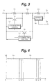
- Fig. 3 shows the second embodiment of the invention.
- Resistors 11, 12, and 13 are serially inserted between the input terminal Ti and output terminal To.
- the resistor 11 is provided between an emitter and a collector of a pnp-type transistor 14 and a ⁇ V11 detecting/control circuit 15' is also provided therebetween.
- a base of the transistor 14 is connected to the ⁇ V11 detecting/control circuit 15' and controlled by the ⁇ V11 detecting/control circuit 15'.
- the ⁇ V11 detecting/control circuit 15' detects a current from a voltage across the resistor 11.
- a predetermined potential difference ⁇ V11
- the resistors 11 and 12 are serially provided between an emitter and a collector of a pnp-type transistor 16 and a ⁇ V12 detecting/control circuit 17' is also provided therebetween.
- a base of the transistor 16 is connected to the ⁇ V12 detecting/control circuit 17'.
- the transistor 16 is controlled by the ⁇ V12 detecting/control circuit 17'.
- the ⁇ V12 detecting/control circuit 17' detects a current from a voltage across the resistors 11 and 12 provided serially.
- a predetermined potential difference ( ⁇ V12) is detected by the ⁇ V12 detecting/control circuit 17', a signal for raising an impedance of the transistor 16 is supplied to the base of the transistor 16.
- a signal for reducing the impedance of the transistor 14 is supplied from the ⁇ V12 detecting/control circuit 17' to the ⁇ V11 detecting/control circuit 15'.
- a current detecting circuit 18 is connected to both ends of the resistor 13 and a current is detected from a voltage across the resistor 13.
- the current detecting circuit 18 transmits a signal according to the detected current to, for example, a microcomputer through a terminal Ta.
- ⁇ V11 detecting/control circuit 15' has been used in the second embodiment, a constant current detecting/control circuit can be used, a ⁇ V11 detecting circuit and a control circuit can be also used, or a constant current detecting circuit and a control circuit can be also used.
- ⁇ V12 detecting/control circuit 17' has been used, a constant current detecting circuit and a control circuit can be used, a ⁇ V12 detecting circuit and a control circuit can be also used, or a constant current detecting circuit and a control circuit can be also used.
- a voltage drop of the resistor 11 is set to be lower than ⁇ V11.
- a voltage drop of the resistor 12 is set to be lower than ⁇ V12.
- Broken lines shown in Fig. 4 indicate a voltage drop Va due to the resistor 11 and a voltage drop Vb due to the resistor 12.
- the resistor 11 is selected so as to obtain a voltage value higher than ⁇ V11 until a current Ib.
- the current is a current after the current Ib, for example, a current Ic
- the transistor 14 is turned on. That is, the current at which the transistor 14 is turned on is selected so as to obtain a current value larger than the current Ib.
- the resistor 12 is selected so as to obtain a voltage value higher than ⁇ V12 until a current Ie.
- the current is a current after the current le, for example, a current If, the transistor 16 is turned on. That is, the current at which the transistor 16 is turned on is selected so as to obtain a current value larger than the current Ie.
- the transistor 14 is turned on by a current smaller than the current Ib and the transistor 16 is turned on by a current smaller than the current le.
- the transistor when a predetermined current is detected, the transistor is turned on or off.
- the current cannot be detected from the voltage across the resistor 11.
- the maximum current I12 which can be detected from the resistor 12 satisfies a relation of I12 > I11, the current I11 is extracted from the current I12 in the embodiment. Therefore, the transistor 14 is turned on or off by the extracted current I11.
- the current I11 is extracted from the maximum current I13 which can be detected from the resistor 13 and the on/off operations of the transistor 16 is controlled by the extracted current I12.
- the resistors 11, 12, and 13 are provided in parallel between the input terminal Ti and output terminal To, the transistor 14 is provided between the resistor 12 and input terminal Ti, and the transistor 16 is provided between the resistor 13 and input terminal Ti.
- a terminal Tb led out from the base of the transistor 14 is connected to the control circuit, and a terminal Tc led out from the base of the transistor 16 is connected to the control circuit.
- R11 > R12 > R13 among a resistance value R11 of the resistor 11, a resistance value R12 of the resistor 12, and a resistance value R13 of the resistor 13.
- a constant current is detected from the voltage across the resistor 11 for a period of time from a time point ta to a time point tb shown in Fig. 6.
- the transistor 14 since the transistor 14 operates by ⁇ V, it is turned on after the time point tb.
- the transistor 16 since the transistor 16 also operates by ⁇ V as mentioned above, it is turned on after a time point tc. In this instance, the transistor 14 is turned off. Even if the transistor 14 is turned off, a large current can be detected in the resistor 13. Since R11 >> R13, the accurate current can be detected from the voltage across the resistor 13.
- Fig. 7 shows a block diagram of the first example to which the invention is applied.
- the transistor 3 can be also controlled by a value of the current flowing in the resistor 2.
- the current flowing in the resistor 2 is detected from the voltage across the resistor 2 by the current detecting circuit 6.
- a signal is supplied from the current detecting circuit 6 to an impedance varying circuit 21.
- the impedance varying circuit 21 supplies a signal for reducing the impedance of the transistor 3 from the control circuit 4 to the base of the transistor 3 through the constant current detecting circuit 5 in order to reduce the impedance of the transistor 3.
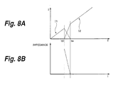
- the current I1 flowing in the resistor 1 starts to decrease at a time point td and a current I2 flowing in the resistor 2 starts to rise.
- the current I1 reaches almost zero and, as for the current I2, the supplied current can be detected.
- the impedance of the transistor 3 starts to decrease.
- the impedance of the transistor 3 reaches almost zero.
- Fig. 9 shows a block diagram of the second example to which the invention is applied.
- the current flowing in the resistor 12 is detected by a current detecting circuit 31 and when the detected current is equal to a predetermined value, a signal is supplied to an impedance varying circuit 32.
- the impedance varying circuit 32 supplies a signal to the base of the transistor 14 through a constant current control circuit 15 in order to reduce the impedance of the transistor 14.
- the current detecting circuit 18 detects the current flowing in the resistor 13. When the detected current is equal to a predetermined value, a signal is supplied to an impedance varying circuit 33.
- the impedance varying circuit 33 supplies a signal to the base of the transistor 16 through a constant current control circuit 17 in order to reduce the impedance of the transistor 16.
- Fig. 10 shows a block diagram of the third example to which the invention is applied.
- a current detecting circuit 41 detects the current flowing in the resistor 12. When the detected current reaches a predetermined value, a signal is supplied to the constant current control circuit 15 through a constant current varying circuit 42 so as to reduce a detected constant current in order to decrease the current flowing in the resistor 11.
- the current detecting circuit 18 detects the current flowing in the resistor 13. When the detected current reaches a predetermined value, a signal is supplied to the constant current control circuit 17 through a constant current varying circuit 43 so as to reduce a detected constant current in order to decrease the current flowing in the resistor 12.
- Fig. 11 shows the fourth embodiment of the invention.
- the fourth embodiment can be also used in the case where the voltages and currents are supplied from both directions.
- a voltage and a current are supplied from a terminal Tio1 or Tio2.
- the current flowing in the resistor 1 is detected by a transistor 3a, a control circuit 4a, and a detecting circuit 5a.
- the current flowing in the resistor 1 is detected by a transistor 3b, a control circuit 4b, and a detecting circuit 5b.
- the current flowing in the resistor 2 is detected by the current detecting circuit 6.
- the on/off operations of the transistor 3a or 3b are controlled in accordance with the detected current.
- transistors 3a and 3b are used in the fourth embodiment, an FET can be also used in place of each of the transistors.
- ⁇ V is set in consideration of the voltage drop of about 0.6V.
- the detecting circuits 5a and 5b are used in the fourth embodiment, as mentioned above, the constant current detecting circuit can be used in place of each of them or the ⁇ V detecting circuit can be also used.
- Fig. 12 shows another example of the fourth embodiment.
- a microcomputer 51 when the current of the predetermined value is detected by each of the constant current detecting circuits 5 and 6, a signal is supplied from the constant current detecting circuit 5.
- the microcomputer 51 controls the transistors 3a and 3b through control circuits 4a and 4b in accordance with the supplied signal.
- the control of the transistors 3a and 3b can be set to various control methods on the basis of the current which is obtained from the voltage across the resistor 1 and/or the current which is obtained from the voltage across the resistor 2.
- Fig. 13 shows the fifth embodiment of the invention.
- a signal is supplied to a control circuit 61.
- the control circuit 61 controls the on/off operations of the transistor 3 through the control circuit 4 in response to the supplied signal.
- the control circuit 61 changes the predetermined value of the current which flows in the resistor 1 and is detected by a current detecting circuit 62, or the control circuit 61 stops the detecting operation of the current detecting circuit 62 in accordance with the supplied signal.
- the current flowing in the resistor 1 is detected by the current detecting circuit 62.
- the signal is outputted from a terminal Te.
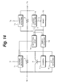
- Fig. 14 shows the first example of the sixth embodiment of the invention.
- a current is detected by a current detecting circuit 71. When the detected current is equal to a predetermined value, a signal is outputted from a terminal Tf.
- a current is detected by a current detecting circuit 72. When the detected current is equal to a predetermined value, a signal is outputted from a terminal Tg.
- the current detecting circuit 6 detects the current flowing in the resistor 2.
- a signal (b) is supplied from the current detecting circuit 6 to a reset circuit 73.
- a signal (a) is supplied from the current detecting circuit 6 to a detection stop circuit 74 and a switch operating circuit 75.
- the reset circuit 73 supplies a reset signal to the detection stop circuit 74 and switch operating circuit 75.
- the detection stop circuit 74 stops the detecting operation of the current detecting circuit 71.
- the detection stop circuit 74 allows the current detecting circuit 71 to execute the detecting operation.
- the switch operating circuit 75 supplies a signal to the control circuit 4 so as to turn on the transistor 3.
- the switch operating circuit 75 supplies a signal to the control circuit 4 so as to turn off the transistor 3.
- Fig. 15 shows the second example of the sixth embodiment of the invention. As shown in Fig. 15, the resistors 1 and 2 can be also arranged in parallel.
- ⁇ V detecting circuit 5' shown in Fig. 15 detects ⁇ V from both ends of the resistor 1, since there is the relation of R1 > R2 between the resistors 1 and 2, ⁇ V can be also detected from both ends of the emitter and collector of the transistor 3.
- Fig. 16 shows the third example of the sixth embodiment of the invention.
- a switching circuit is further provided for the control of ⁇ V.
- the current detecting circuit 6 detects the current flowing in the resistor 2.
- the signal (b) is supplied from the current detecting circuit 6 to a detection operating circuit 81 and a switch OFF circuit 84.
- the signal (a) is supplied from the current detecting circuit 6 to a detection stop circuit 82 and a switch ON circuit 83.
- the current detecting circuit 71 detects the current flowing in the resistor 1.
- the current detecting circuit 71 stops the operation for detecting the current.
- a switching circuit 85 is turned on.
- a switching circuit 85 is turned off.
- step S1 the current is detected by the current detecting circuit 6.
- step S2 whether the detected current is equal to or larger than the second current value or not is discriminated.
- a processing routine advances to step S3.
- step S3 a delay of a time constant ⁇ t is made.
- step S4 the detecting operation of the current detecting circuit 71 is stopped.
- step S5 the delay of the time constant ⁇ t is made.
- step S6 the signal to turn on the transistor 3 is supplied to the control circuit 4.
- step S7 the current is detected by the current detecting circuit 6.
- step S8 whether the detected current is equal to or less than the first current value or not is discriminated.
- a processing routine advances to step S9.
- step S9 the delay of the time constant ⁇ t is made.
- step S10 the signal to turn off the transistor 3 is supplied to the control circuit 4.
- step S11 the delay of the time constant ⁇ t is made.
- step S12 the detecting operation of the current detecting circuit 71 is executed. A processing routine is returned to step S1.
- the time constant ⁇ t in steps S3, S5, S9, and S11 is not the delay that is always necessary. Such a control can be omitted in dependence on its setting method.
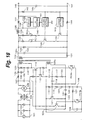
- Fig. 18 shows an embodiment of a circuit diagram of an AC adapter to which the invention is applied.
- a commercially available power source which is supplied from a commercially available power source 101 passes through a rectifying circuit comprising a capacitor 102, a noise remover 103, a filter 104, a diode bridge 105, and a capacitor 106.
- a resistor 107, a capacitor 108, a resistor 109, a diode 110, a pnp-type transistor 112, and a resistor 111 are provided between the rectifying circuit and a primary winding 129 1 of a transformer 129.
- the transistor 112, a transistor 113, and a resistor 114 are provided between the primary winding 129 1 and a secondary winding 129 2 .
- a receiving unit for receiving a signal which is transmitted from the secondary side of the transformer 129 is provided for the secondary winding 129 2 .
- a first receiving unit comprises: a receiving unit which is formed by a photodiode PC1b of a photocoupler and an npn-type transistor 124; and a power supplying unit which is formed by a resistor 116, a resistor 119, a diode 120, a diode 125, a capacitor 126, a resistor 127, and a capacitor 128.
- the first receiving unit receives a signal showing that a load has been connected on the secondary side.
- a second receiving unit comprises: a receiving unit which is formed by a photodiode PC2b of a photocoupler and an npn-type transistor 121; and a power supplying unit which is formed by a capacitor 115, a resistor 117, a diode 130, and a capacitor 118.
- the second receiving unit receives a signal showing that a constant voltage and a constant current have been detected on the secondary side.
- a capacitor 122 and a resistor 123 are provided between the receiving unit of the first and second receiving units and the power supplying unit.
- a rectifying circuit comprising a diode 131 and a capacitor 132 is provided for a ternary winding 129 3 serving as a secondary side of the transformer.
- a Zener diode 133 is provided in parallel with the rectifying circuit.
- a first transmitting unit which is formed by a resistor 134, a light emitting diode PC1a of a photocoupler, and an npn-type transistor 148 is provided in parallel with the rectifying circuit.
- a second transmitting unit which is formed by a resistor 135, a light emitting diode PC2a of a photocoupler, and an npn-type transistor 149 is also provided in parallel with the rectifying circuit.
- An inductor 136 and a resistor 137 are serially provided between the rectifying circuit and an output terminal 146.
- a resistor 144 is provided between the rectifying circuit and an output terminal 147.
- the resistor 137 is used to detect the small current.
- a ⁇ V detecting circuit 140 detects ⁇ V from a voltage across the resistor 137. When a predetermined value is detected by the ⁇ V detecting circuit 140, a pnp-type transistor 138 is turned on through a control circuit 139. Similarly, when a predetermined value is detected by the ⁇ V detecting circuit 140, a signal is supplied to a voltage current detecting circuit 141.
- a resistor 142 and a capacitor 145 are provided in parallel between the output terminals 146 and 147.
- the voltage current detecting circuit 141 detects a voltage and/or a current from a node of the resistor 142 and output terminal 147.
- the npn-type transistor 148 is controlled on the basis of the detected voltage and/or current and the signal obtained from the ⁇ V detecting circuit 140.
- the transistor 148 is turned on, the light emitting diode PC1a is turned on, and a signal showing that a load has been connected is transmitted to the primary side.
- a current detecting circuit 143 detects a current from a voltage across the resistor 144.
- the transistor 149 When the detected voltage is equal to a predetermined value, the transistor 149 is turned on. When the transistor 149 is turned on, the light emitting diode PC2a is turned on, and a signal showing that a constant current and a constant voltage have been detected is transmitted to the primary side.
- a detecting range of the current can be enlarged. Since it is possible to construct the apparatus so that it is not influenced by the different detecting circuits, the loss can be reduced and, further, detection errors can be decreased.
Landscapes
- Engineering & Computer Science (AREA)
- Power Engineering (AREA)
- Physics & Mathematics (AREA)
- General Physics & Mathematics (AREA)
- Measurement Of Current Or Voltage (AREA)
Abstract
Description
- The invention relates to a current detecting apparatus which can precisely detect a current in a range from a small current to a large current and to a control method for such an apparatus.
- Hitherto, as a method of detecting a current, an example of detecting a current by using two power sources having a potential difference has been disclosed in JP-A-10-28338 by the same applicant of the present invention. According to JP-A-10-28338, it is intended to detect a value of a current at the time of charging a secondary battery. When it is explained with reference to Fig. 19, a voltage E1 of a
power source 201 and a voltage E2 of apower source 203 are set so that a potential difference is equal to ΔV. It is now assumed that thepower source 201 can output a low voltage and a large current and thepower source 203 can output a high voltage and a small current. A current is detected from a voltage across aresistor 202 having a small resistance value. A current is detected from a voltage across aresistor 204 having a large resistance value. - However, in the example of Fig. 19, there is a problem such that when the small current and the large current are detected, they exercise an influence on each other.
- It is, therefore, an object of the invention to provide a current detecting apparatus in which since a detecting range of a current can be enlarged and the current can be independently detected, its influence can be minimized, errors can be reduced, and the loss can be decreased and to provide a control method of such an apparatus.
- According to the first aspect of the invention, there is provided a current detecting apparatus comprising: a first resistor provided between an input terminal and an output terminal; first switching means provided in parallel with the first resistor; control means for controlling the switching means: first detecting means for detecting a current flowing in the first resistor or a potential difference which is caused in the first resistor; a second resistor provided so as to be serial to at least the first switching means; and second detecting means for detecting a current flowing in the second resistor or a potential difference which is caused in the second resistor, wherein the control means turns off the switching means when the current or potential difference that is equal to or larger than a first predetermined value is detected by the first detecting means and turns on the switching means when the current or potential difference that is equal to or smaller than a second predetermined value is detected by the second detecting means, and the first and second detecting means outputs the detected current or potential difference.
- According to the second aspect of the invention, there is provided a control method for a current detecting apparatus comprising: a first resistor provided between an input terminal and an output terminal; switching means provided in parallel with the first resistor; control means for controlling the switching means; first detecting means for detecting a current flowing in the first resistor or a potential difference which is caused in the first resistor; a second resistor provided so as to be serial to at least the switching means; and second detecting means for detecting a current flowing in the second resistor or a potential difference which is caused in the second resistor, wherein when the current or potential difference that is equal to or larger than a first predetermined value is detected by the first detecting means, the switching means is turned off, when the current or potential difference that is equal to or smaller than a second predetermined value is detected by the second detecting means, the switching means is turned on, and the first and second detecting means outputs the detected current or potential difference.
- Owing to the switching means provided in parallel with the first register arranged between the input terminal and the output terminal, the current or potential difference which is obtained from the first resistor and the current or potential difference which is obtained from the second resistor can be detected so that the first and second resistors are not influenced each other.
- The above and other objects and features of the present invention will become apparent from the following detailed description and the appended claims with reference to the accompanying drawings.
-
- Fig. 1 is a block diagram of the first embodiment to which the invention is applied;
- Fig. 2 is a block diagram of another example of the first embodiment to which the invention is applied;
- Fig. 3 is a block diagram of the second embodiment to which the invention is applied;
- Fig. 4 shows an example of a voltage/current characteristics diagram for explaining the invention;
- Fig. 5 is a block diagram of the third embodiment to which the invention is applied;
- Fig. 6 shows an example of a characteristics diagram for explaining the invention;
- Fig. 7 is a block diagram of the first example to which the invention is applied;
- Figs. 8A and 8B show examples of characteristics diagrams for explaining the invention;
- Fig. 9 is a block diagram of the second example to which the invention is applied;
- Fig. 10 is a block diagram of the third example to which the invention is applied;
- Fig. 11 is a block diagram of the fourth embodiment to which the invention is applied;
- Fig. 12 is a block diagram of another example of the fourth embodiment to which the invention is applied;
- Fig. 13 is a block diagram of the fifth embodiment to which the invention is applied;
- Fig. 14 is a block diagram of the first example of the sixth embodiment to which the invention is applied;
- Fig. 15 is a block diagram of the second example of the sixth embodiment to which the invention is applied;
- Fig. 16 is a block diagram of the third example of the sixth embodiment to which the invention is applied;
- Fig. 17 is a flowchart for explaining the operation in the sixth embodiment to which the invention is applied;
- Fig. 18 is a block diagram to which the invention is applied; and
- Fig. 19 is a block diagram of an example of conventional current detection.
-
- An embodiment of the invention will now be described hereinbelow with reference to the drawings. Component elements having substantially the same functions and signals having substantially the same effects in the diagrams are designated by the same reference numerals and their overlapped description is omitted. Fig. 1 shows the first embodiment to which the invention is applied. Rectified voltage and current are supplied from an input terminal Ti.
Resistors resistor 1 is compared with a resistance value R2 of theresistor 2, there is a relation of R1 > R2. - The
resistor 1 is provided between an emitter and a collector of a pnp-type transistor 3 and a constant current detectingcircuit 5 is also provided therebetween. A base of thetransistor 3 is connected to acontrol circuit 4 and controlled by thecontrol circuit 4. The constantcurrent detecting circuit 5 detects a current from a voltage across theresistor 1. A current detectingcircuit 6 is connected to both ends of theresistor 2 and detects a current from a voltage across theresistor 2. The constantcurrent detecting circuit 5 detects a small current and the current detectingcircuit 6 detects a large current. - When the small current is detected by the constant current detecting
circuit 5, a signal is supplied to thecontrol circuit 4. Thecontrol circuit 4 supplies a signal for raising an impedance of thetransistor 3 to the base of thetransistor 3. Therefore, no current flows in thetransistor 3. At this time, the impedance of thetransistor 3 is controlled so as not to be equal to or larger than (a current I1 flowing in theresistor 1 × the resistance value R1 of the resistor 1). - That is, when the current of a predetermined value is detected by the constant current detecting
circuit 5 and thetransistor 3 is turned off, the constant current detectingcircuit 5 cannot detect a subsequent current change. Therefore, as a signal to turn on thetransistor 3, a signal according to the current detected by the current detectingcircuit 6 is outputted. - Fig. 2 shows another example of the first embodiment. In another example shown in Fig. 2, a ΔV detecting circuit 5' is used in place of the constant current detecting
circuit 5. The ΔV detecting circuit 5' detects a potential difference of the voltage across theresistor 1, that is, ΔV. When ΔV is detected, a signal is supplied to thecontrol circuit 4. Thecontrol circuit 4 supplies the signal for raising the impedance of thetransistor 3 to the base of thetransistor 3. As mentioned above, even when ΔV is detected, an effect that is similar to that by the constant current detection can be obtained. - Fig. 3 shows the second embodiment of the invention.
Resistors resistor 11 is provided between an emitter and a collector of a pnp-type transistor 14 and a ΔV11 detecting/control circuit 15' is also provided therebetween. A base of thetransistor 14 is connected to the ΔV11 detecting/control circuit 15' and controlled by the ΔV11 detecting/control circuit 15'. The ΔV11 detecting/control circuit 15' detects a current from a voltage across theresistor 11. When a predetermined potential difference (ΔV11) is detected by the ΔV11 detecting/control circuit 15', a signal for raising an impedance of thetransistor 14 is supplied to the base of thetransistor 14. - The
resistors type transistor 16 and a ΔV12 detecting/control circuit 17' is also provided therebetween. A base of thetransistor 16 is connected to the ΔV12 detecting/control circuit 17'. Thetransistor 16 is controlled by the ΔV12 detecting/control circuit 17'. The ΔV12 detecting/control circuit 17' detects a current from a voltage across theresistors transistor 16 is supplied to the base of thetransistor 16. Further, a signal for reducing the impedance of thetransistor 14 is supplied from the ΔV12 detecting/control circuit 17' to the ΔV11 detecting/control circuit 15'. - A current detecting
circuit 18 is connected to both ends of theresistor 13 and a current is detected from a voltage across theresistor 13. The current detectingcircuit 18 transmits a signal according to the detected current to, for example, a microcomputer through a terminal Ta. - When ΔV11 is detected as a potential difference of the voltage across the
resistor 11 by the ΔV11 detecting/control circuit 15' as mentioned above, a current which is equal to or larger than a maximum current I11 flowing in theresistor 11 does not flow. When ΔV12 is detected as a potential difference of the voltage across theresistors resistor 12 does not flow. Actually, since the impedance of thetransistor 14 is lowered, ΔV12 is derived from a potential difference of the voltage across theresistor 12. - Although the ΔV11 detecting/control circuit 15' has been used in the second embodiment, a constant current detecting/control circuit can be used, a ΔV11 detecting circuit and a control circuit can be also used, or a constant current detecting circuit and a control circuit can be also used. Although the ΔV12 detecting/control circuit 17' has been used, a constant current detecting circuit and a control circuit can be used, a ΔV12 detecting circuit and a control circuit can be also used, or a constant current detecting circuit and a control circuit can be also used.
- A voltage drop of the
resistor 11 is set to be lower than ΔV11. A voltage drop of theresistor 12 is set to be lower than ΔV12. Broken lines shown in Fig. 4 indicate a voltage drop Va due to theresistor 11 and a voltage drop Vb due to theresistor 12. As for the voltage drop Va, theresistor 11 is selected so as to obtain a voltage value higher than ΔV11 until a current Ib. When the current is a current after the current Ib, for example, a current Ic, thetransistor 14 is turned on. That is, the current at which thetransistor 14 is turned on is selected so as to obtain a current value larger than the current Ib. As for the voltage drop Vb, theresistor 12 is selected so as to obtain a voltage value higher than ΔV12 until a current Ie. When the current is a current after the current le, for example, a current If, thetransistor 16 is turned on. That is, the current at which thetransistor 16 is turned on is selected so as to obtain a current value larger than the current Ie. - It is also possible to turn on the
transistor 14 by detecting ΔV11 from theresistor 11 and to turn on thetransistor 16 by detecting ΔV12 from theresistor 12. In this case, thetransistor 14 is turned on by a current smaller than the current Ib and thetransistor 16 is turned on by a current smaller than the current le. - Further, also in the case where the apparatus has the constant current detecting circuit, similarly, in order to reduce the loss of the transistor, when a predetermined current is detected, the transistor is turned on or off. When
transistor 14 is turned on, the current cannot be detected from the voltage across theresistor 11. However, since the maximum current I12 which can be detected from theresistor 12 satisfies a relation of I12 > I11, the current I11 is extracted from the current I12 in the embodiment. Therefore, thetransistor 14 is turned on or off by the extracted current I11. Similarly, the current I11 is extracted from the maximum current I13 which can be detected from theresistor 13 and the on/off operations of thetransistor 16 is controlled by the extracted current I12. - The third embodiment of the invention will be described with reference to Fig. 5. In the third embodiment, the
resistors transistor 14 is provided between theresistor 12 and input terminal Ti, and thetransistor 16 is provided between theresistor 13 and input terminal Ti. Although not shown, a terminal Tb led out from the base of thetransistor 14 is connected to the control circuit, and a terminal Tc led out from the base of thetransistor 16 is connected to the control circuit. At this time, it is assumed that there is a relation of R11 > R12 > R13 among a resistance value R11 of theresistor 11, a resistance value R12 of theresistor 12, and a resistance value R13 of theresistor 13. - A constant current is detected from the voltage across the
resistor 11 for a period of time from a time point ta to a time point tb shown in Fig. 6. As mentioned above, since thetransistor 14 operates by ΔV, it is turned on after the time point tb. Similarly, since thetransistor 16 also operates by ΔV as mentioned above, it is turned on after a time point tc. In this instance, thetransistor 14 is turned off. Even if thetransistor 14 is turned off, a large current can be detected in theresistor 13. Since R11 >> R13, the accurate current can be detected from the voltage across theresistor 13. - Fig. 7 shows a block diagram of the first example to which the invention is applied. As shown in Fig. 7, the
transistor 3 can be also controlled by a value of the current flowing in theresistor 2. In the example shown in Fig. 7, the current flowing in theresistor 2 is detected from the voltage across theresistor 2 by the current detectingcircuit 6. When the detected current is equal to a predetermined value, a signal is supplied from the current detectingcircuit 6 to animpedance varying circuit 21. Theimpedance varying circuit 21 supplies a signal for reducing the impedance of thetransistor 3 from thecontrol circuit 4 to the base of thetransistor 3 through the constant current detectingcircuit 5 in order to reduce the impedance of thetransistor 3. - As shown in Fig. 8A, the current I1 flowing in the
resistor 1 starts to decrease at a time point td and a current I2 flowing in theresistor 2 starts to rise. At a time point te, the current I1 reaches almost zero and, as for the current I2, the supplied current can be detected. At the time point td, as shown in Fig. 8B, the impedance of thetransistor 3 starts to decrease. At the time point te, the impedance of thetransistor 3 reaches almost zero. By this method, the detection loss can be reduced. - Fig. 9 shows a block diagram of the second example to which the invention is applied. As shown in Fig. 9, also in case of using the three
resistors resistor 12 is detected by a current detectingcircuit 31 and when the detected current is equal to a predetermined value, a signal is supplied to animpedance varying circuit 32. Theimpedance varying circuit 32 supplies a signal to the base of thetransistor 14 through a constantcurrent control circuit 15 in order to reduce the impedance of thetransistor 14. - The current detecting
circuit 18 detects the current flowing in theresistor 13. When the detected current is equal to a predetermined value, a signal is supplied to animpedance varying circuit 33. Theimpedance varying circuit 33 supplies a signal to the base of thetransistor 16 through a constantcurrent control circuit 17 in order to reduce the impedance of thetransistor 16. - Also in the block diagram shown in Fig. 9, in a manner similar to the circuit of the block diagram shown in Fig. 7 mentioned above, when the current flowing in the
resistor 12 is equal to a predetermined value, the impedance of thetransistor 14 starts to decrease. Further, when the current flowing in theresistor 13 is equal to a predetermined value, a control is made so as to start to decrease the impedance of thetransistor 16. - Fig. 10 shows a block diagram of the third example to which the invention is applied. A current detecting
circuit 41 detects the current flowing in theresistor 12. When the detected current reaches a predetermined value, a signal is supplied to the constantcurrent control circuit 15 through a constant current varyingcircuit 42 so as to reduce a detected constant current in order to decrease the current flowing in theresistor 11. The current detectingcircuit 18 detects the current flowing in theresistor 13. When the detected current reaches a predetermined value, a signal is supplied to the constantcurrent control circuit 17 through a constant current varyingcircuit 43 so as to reduce a detected constant current in order to decrease the current flowing in theresistor 12. - Fig. 11 shows the fourth embodiment of the invention. The fourth embodiment can be also used in the case where the voltages and currents are supplied from both directions. A voltage and a current are supplied from a terminal Tio1 or Tio2. When the voltage and current are supplied from the terminal Tio1, the current flowing in the
resistor 1 is detected by atransistor 3a, acontrol circuit 4a, and a detectingcircuit 5a. When the voltage and current are supplied from the terminal Tio2, the current flowing in theresistor 1 is detected by atransistor 3b, acontrol circuit 4b, and a detectingcircuit 5b. The current flowing in theresistor 2 is detected by the current detectingcircuit 6. The on/off operations of thetransistor - Although the
transistors - Although the detecting
circuits - Fig. 12 shows another example of the fourth embodiment. In a
microcomputer 51, when the current of the predetermined value is detected by each of the constant current detectingcircuits circuit 5. Themicrocomputer 51 controls thetransistors control circuits - As mentioned above, by using the microcomputer, the control of the
transistors resistor 1 and/or the current which is obtained from the voltage across theresistor 2. - Fig. 13 shows the fifth embodiment of the invention. In the current detecting
circuit 6, when the detected current is equal to a predetermined value, a signal is supplied to acontrol circuit 61. Thecontrol circuit 61 controls the on/off operations of thetransistor 3 through thecontrol circuit 4 in response to the supplied signal. Similarly, thecontrol circuit 61 changes the predetermined value of the current which flows in theresistor 1 and is detected by a current detectingcircuit 62, or thecontrol circuit 61 stops the detecting operation of the current detectingcircuit 62 in accordance with the supplied signal. The current flowing in theresistor 1 is detected by the current detectingcircuit 62. When the detected current is equal to the predetermined value, the signal is outputted from a terminal Te. - Fig. 14 shows the first example of the sixth embodiment of the invention. A current is detected by a current detecting
circuit 71. When the detected current is equal to a predetermined value, a signal is outputted from a terminal Tf. A current is detected by a current detectingcircuit 72. When the detected current is equal to a predetermined value, a signal is outputted from a terminal Tg. The current detectingcircuit 6 detects the current flowing in theresistor 2. When the detected current is equal to or less than a first current value, a signal (b) is supplied from the current detectingcircuit 6 to areset circuit 73. When the detected current is equal to or less than a second current value larger than the first current value, a signal (a) is supplied from the current detectingcircuit 6 to adetection stop circuit 74 and aswitch operating circuit 75. - The
reset circuit 73 supplies a reset signal to thedetection stop circuit 74 and switchoperating circuit 75. When the signal (a) is supplied, thedetection stop circuit 74 stops the detecting operation of the current detectingcircuit 71. When the signal is supplied from thereset circuit 73, thedetection stop circuit 74 allows the current detectingcircuit 71 to execute the detecting operation. When the signal (a) is supplied, theswitch operating circuit 75 supplies a signal to thecontrol circuit 4 so as to turn on thetransistor 3. When the signal is supplied from thereset circuit 73, theswitch operating circuit 75 supplies a signal to thecontrol circuit 4 so as to turn off thetransistor 3. - Fig. 15 shows the second example of the sixth embodiment of the invention. As shown in Fig. 15, the
resistors - Although the ΔV detecting circuit 5' shown in Fig. 15 detects ΔV from both ends of the
resistor 1, since there is the relation of R1 > R2 between theresistors transistor 3. - Fig. 16 shows the third example of the sixth embodiment of the invention. In the third example, a switching circuit is further provided for the control of ▵V. The current detecting
circuit 6 detects the current flowing in theresistor 2. When the detected current is equal to or less than the first current value, the signal (b) is supplied from the current detectingcircuit 6 to adetection operating circuit 81 and aswitch OFF circuit 84. When the detected current is equal to or larger than a second current value larger than the first current value, the signal (a) is supplied from the current detectingcircuit 6 to adetection stop circuit 82 and a switch ONcircuit 83. - When the signal is supplied from the
detection operating circuit 81, the current detectingcircuit 71 detects the current flowing in theresistor 1. When the signal is supplied from thedetection stop circuit 82, the current detectingcircuit 71 stops the operation for detecting the current. When the signal is supplied from the switch ONcircuit 83, a switchingcircuit 85 is turned on. When the signal is supplied from the switch OFFcircuit 84, a switchingcircuit 85 is turned off. - The operation in the sixth embodiment will now be described with reference to a flowchart shown in Fig. 17. In step S1, the current is detected by the current detecting
circuit 6. In step S2, whether the detected current is equal to or larger than the second current value or not is discriminated. When it is decided that it is equal to or larger than the second current value, a processing routine advances to step S3. When it is determined that it is less than the second current value, a processing routine is returned to step S1. In step S3, a delay of a time constant Δt is made. In step S4, the detecting operation of the current detectingcircuit 71 is stopped. In step S5, the delay of the time constant Δt is made. In step S6, the signal to turn on thetransistor 3 is supplied to thecontrol circuit 4. - In step S7, the current is detected by the current detecting
circuit 6. In step S8, whether the detected current is equal to or less than the first current value or not is discriminated. When it is decided that it is equal to or less than the first current value, a processing routine advances to step S9. When it is determined that it is larger than the first current value, a processing routine is returned to step S7. In step S9, the delay of the time constant Δt is made. In step S10, the signal to turn off thetransistor 3 is supplied to thecontrol circuit 4. In step S11, the delay of the time constant Δt is made. In step S12, the detecting operation of the current detectingcircuit 71 is executed. A processing routine is returned to step S1. - In the flowchart shown in Fig. 17, the time constant Δt in steps S3, S5, S9, and S11 is not the delay that is always necessary. Such a control can be omitted in dependence on its setting method.
- Fig. 18 shows an embodiment of a circuit diagram of an AC adapter to which the invention is applied. A commercially available power source which is supplied from a commercially
available power source 101 passes through a rectifying circuit comprising acapacitor 102, anoise remover 103, afilter 104, adiode bridge 105, and acapacitor 106. Aresistor 107, acapacitor 108, aresistor 109, a diode 110, a pnp-type transistor 112, and aresistor 111 are provided between the rectifying circuit and a primary winding 1291 of atransformer 129. Thetransistor 112, atransistor 113, and aresistor 114 are provided between the primary winding 1291 and a secondary winding 1292. - A receiving unit for receiving a signal which is transmitted from the secondary side of the
transformer 129 is provided for the secondary winding 1292. A first receiving unit comprises: a receiving unit which is formed by a photodiode PC1b of a photocoupler and an npn-type transistor 124; and a power supplying unit which is formed by aresistor 116, aresistor 119, adiode 120, adiode 125, acapacitor 126, aresistor 127, and acapacitor 128. The first receiving unit receives a signal showing that a load has been connected on the secondary side. A second receiving unit comprises: a receiving unit which is formed by a photodiode PC2b of a photocoupler and an npn-type transistor 121; and a power supplying unit which is formed by acapacitor 115, aresistor 117, adiode 130, and acapacitor 118. The second receiving unit receives a signal showing that a constant voltage and a constant current have been detected on the secondary side. Acapacitor 122 and aresistor 123 are provided between the receiving unit of the first and second receiving units and the power supplying unit. - A rectifying circuit comprising a
diode 131 and acapacitor 132 is provided for a ternary winding 1293 serving as a secondary side of the transformer. AZener diode 133 is provided in parallel with the rectifying circuit. A first transmitting unit which is formed by aresistor 134, a light emitting diode PC1a of a photocoupler, and an npn-type transistor 148 is provided in parallel with the rectifying circuit. A second transmitting unit which is formed by aresistor 135, a light emitting diode PC2a of a photocoupler, and an npn-type transistor 149 is also provided in parallel with the rectifying circuit. - An
inductor 136 and aresistor 137 are serially provided between the rectifying circuit and anoutput terminal 146. Aresistor 144 is provided between the rectifying circuit and anoutput terminal 147. Theresistor 137 is used to detect the small current. AΔV detecting circuit 140 detects ΔV from a voltage across theresistor 137. When a predetermined value is detected by theΔV detecting circuit 140, a pnp-type transistor 138 is turned on through acontrol circuit 139. Similarly, when a predetermined value is detected by theΔV detecting circuit 140, a signal is supplied to a voltage current detectingcircuit 141. - A
resistor 142 and acapacitor 145 are provided in parallel between theoutput terminals circuit 141 detects a voltage and/or a current from a node of theresistor 142 andoutput terminal 147. In the voltage current detectingcircuit 141, the npn-type transistor 148 is controlled on the basis of the detected voltage and/or current and the signal obtained from theΔV detecting circuit 140. When thetransistor 148 is turned on, the light emitting diode PC1a is turned on, and a signal showing that a load has been connected is transmitted to the primary side. A current detectingcircuit 143 detects a current from a voltage across theresistor 144. When the detected voltage is equal to a predetermined value, thetransistor 149 is turned on. When thetransistor 149 is turned on, the light emitting diode PC2a is turned on, and a signal showing that a constant current and a constant voltage have been detected is transmitted to the primary side. - According to the invention, a detecting range of the current can be enlarged. Since it is possible to construct the apparatus so that it is not influenced by the different detecting circuits, the loss can be reduced and, further, detection errors can be decreased.
- The present invention is not limited to the foregoing embodiments but many modifications and variations are possible within the scope of the appended claims of the invention.
Claims (7)
- A current detecting apparatus comprising:a first resistor (1) provided between an input terminal (Ti) and an output terminal (To);first switching means (3) provided in parallel with said first resistor;control means (4) for controlling said switching means;first detecting means (5) for detecting a current flowing in said first resistor or a potential difference which is caused in said first resistor;a second resistor (2) provided so as to be serial to at least said first switching means; andsecond detecting means (6) for detecting a current flowing in said second resistor or a potential difference which is caused in said second resistor,wherein said control meansturns off said switching means when the current or potential difference that is equal to or larger than a first predetermined value is detected by said first detecting means andturns on said switching means when the current or potential difference that is equal to or smaller than a second predetermined value is detected by said second detecting means, andsaid first and second detecting means outputs the detected current or potential difference.
- An apparatus according to claim 1, further comprising impedance varying means (21) which can vary an impedance of said first switching means (3).
- An apparatus according to claim 1, further comprising varying means (21) which can vary said first predetermined value of said first detecting means (5).
- An apparatus according to claim 1, further comprising:second switching means (16) provided in parallel with said second resistor (12);a third resistor (13) which is provided so as to be serial to at least said second switching means and has a value smaller than that of said second resistor; andthird detecting means (17) for detecting a current or a small voltage from said third resistor.
- An apparatus according to claim 4, further comprising impedance varying means (33) which can vary an impedance of said second switching means (16).
- An apparatus according to claim 4, further comprising varying means (43) which can vary a third predetermined value of said third detecting means (17).
- A control method for a current detecting apparatus comprising:a first resistor (1) provided between an input terminal (Ti) and an output terminal (To);switching means (3) provided in parallel with said first resistor;control means (4) for controlling said switching means;first detecting means (5) for detecting a current flowing in said first resistor or a potential difference which is caused in said first resistor;a second resistor (2) provided so as to be serial to at least said switching means; andsecond detecting means (6) for detecting a current flowing in said second resistor or a potential difference which is caused in said second resistor,wherein when the current or potential difference that is equal to or larger than a first predetermined value is detected by said first detecting means (5), said switching means (3) is turned off,when the current or potential difference that is equal to or smaller than a second predetermined value is detected by said second detecting means (6), said switching means (3) is turned on, andsaid first and second detecting means (5, 6) outputs the detected current or potential difference.
Applications Claiming Priority (2)
| Application Number | Priority Date | Filing Date | Title |
|---|---|---|---|
| JP2000221642A JP2002040059A (en) | 2000-07-24 | 2000-07-24 | Current detecting device and control method thereof |
| JP2000221642 | 2000-07-24 |
Publications (1)
| Publication Number | Publication Date |
|---|---|
| EP1176425A1 true EP1176425A1 (en) | 2002-01-30 |
Family
ID=18716009
Family Applications (1)
| Application Number | Title | Priority Date | Filing Date |
|---|---|---|---|
| EP01401987A Withdrawn EP1176425A1 (en) | 2000-07-24 | 2001-07-24 | Current detecting apparatus and its control method |
Country Status (5)
| Country | Link |
|---|---|
| US (1) | US6552562B2 (en) |
| EP (1) | EP1176425A1 (en) |
| JP (1) | JP2002040059A (en) |
| KR (1) | KR20020008752A (en) |
| CN (1) | CN1359008A (en) |
Cited By (2)
| Publication number | Priority date | Publication date | Assignee | Title |
|---|---|---|---|---|
| FR2983300A1 (en) * | 2011-11-30 | 2013-05-31 | Valeo Etudes Electroniques | SYSTEM FOR MEASURING CHARGE CURRENT AND DIAGNOSIS OF ABSENCE OF LOAD OR OVERLOAD |
| CN112924743A (en) * | 2021-01-29 | 2021-06-08 | 杭州轨物科技有限公司 | Instrument state detection method based on current data |
Families Citing this family (13)
| Publication number | Priority date | Publication date | Assignee | Title |
|---|---|---|---|---|
| WO2007032755A1 (en) * | 2005-09-09 | 2007-03-22 | Semiconductor Components Industries, L.L.C. | Method of forming a current sense circuit and structure therefor |
| JP4720548B2 (en) * | 2006-03-07 | 2011-07-13 | 住友電装株式会社 | Load abnormality detection system |
| US7973543B2 (en) * | 2008-07-11 | 2011-07-05 | Advantest Corporation | Measurement apparatus, test apparatus and measurement method |
| US8564269B2 (en) * | 2008-12-13 | 2013-10-22 | Hewlett-Packard Development Company, L.P. | Systems and methods for scaling a signal in a power factor correction circuit |
| US9057758B2 (en) * | 2009-12-18 | 2015-06-16 | Semiconductor Energy Laboratory Co., Ltd. | Method for measuring current, method for inspecting semiconductor device, semiconductor device, and test element group |
| US8547146B1 (en) * | 2012-04-04 | 2013-10-01 | Honeywell International Inc. | Overcurrent based power control and circuit reset |
| US9194905B2 (en) * | 2013-04-03 | 2015-11-24 | Denso Corporation | Processing circuit having self-diagnosis function |
| CN104090258B (en) * | 2014-03-19 | 2017-01-04 | 天津市计量监督检测科学研究院 | Micro-electric energy control device |
| JP7127736B2 (en) * | 2019-04-26 | 2022-08-30 | 株式会社オートネットワーク技術研究所 | Current detection device and power supply control device |
| CN110988433A (en) * | 2019-11-19 | 2020-04-10 | 苏州佳世达光电有限公司 | Current detection circuit and current detection method |
| CN112083214B (en) * | 2020-08-28 | 2023-05-16 | 广东电网有限责任公司广州供电局 | Current measuring device for pilot discharge process |
| KR102682917B1 (en) | 2020-10-16 | 2024-07-05 | 삼성에스디아이 주식회사 | Connection test apparatus |
| CN113391111A (en) * | 2021-05-25 | 2021-09-14 | 普源精电科技股份有限公司 | Current detection circuit |
Citations (3)
| Publication number | Priority date | Publication date | Assignee | Title |
|---|---|---|---|---|
| US3699422A (en) * | 1972-02-11 | 1972-10-17 | Honeywell Inc | Automatic battery charger |
| US3735233A (en) * | 1970-08-24 | 1973-05-22 | Globe Union Inc | Battery charger apparatus having multiple modes of operation and automatic switching therebetween |
| JPH0984280A (en) * | 1995-09-14 | 1997-03-28 | Fujitsu Ltd | Power supply monitoring circuit |
Family Cites Families (5)
| Publication number | Priority date | Publication date | Assignee | Title |
|---|---|---|---|---|
| JPH04150767A (en) * | 1990-10-08 | 1992-05-25 | Fuji Electric Co Ltd | Switching power supply circuit |
| US5563541A (en) * | 1994-05-19 | 1996-10-08 | Sony/Tektronix Corporation | Load current detection circuit |
| KR100320672B1 (en) * | 1995-12-30 | 2002-05-13 | 김덕중 | Switching control integrated circuit |
| JPH1029338A (en) | 1996-07-16 | 1998-02-03 | Alps Electric Co Ltd | Thermal transfer printer |
| JP2001161025A (en) * | 1999-11-30 | 2001-06-12 | Ando Electric Co Ltd | Current limiter |
-
2000
- 2000-07-24 JP JP2000221642A patent/JP2002040059A/en active Pending
-
2001
- 2001-07-10 KR KR1020010041184A patent/KR20020008752A/en not_active Withdrawn
- 2001-07-13 US US09/903,576 patent/US6552562B2/en not_active Expired - Fee Related
- 2001-07-24 EP EP01401987A patent/EP1176425A1/en not_active Withdrawn
- 2001-07-24 CN CN01123067A patent/CN1359008A/en active Pending
Patent Citations (3)
| Publication number | Priority date | Publication date | Assignee | Title |
|---|---|---|---|---|
| US3735233A (en) * | 1970-08-24 | 1973-05-22 | Globe Union Inc | Battery charger apparatus having multiple modes of operation and automatic switching therebetween |
| US3699422A (en) * | 1972-02-11 | 1972-10-17 | Honeywell Inc | Automatic battery charger |
| JPH0984280A (en) * | 1995-09-14 | 1997-03-28 | Fujitsu Ltd | Power supply monitoring circuit |
Non-Patent Citations (1)
| Title |
|---|
| PATENT ABSTRACTS OF JAPAN vol. 1997, no. 07 31 July 1997 (1997-07-31) * |
Cited By (4)
| Publication number | Priority date | Publication date | Assignee | Title |
|---|---|---|---|---|
| FR2983300A1 (en) * | 2011-11-30 | 2013-05-31 | Valeo Etudes Electroniques | SYSTEM FOR MEASURING CHARGE CURRENT AND DIAGNOSIS OF ABSENCE OF LOAD OR OVERLOAD |
| WO2013079686A1 (en) * | 2011-11-30 | 2013-06-06 | Valeo Etudes Electroniques | System for measuring a load current and for diagnosing an absence of load or an overload |
| CN112924743A (en) * | 2021-01-29 | 2021-06-08 | 杭州轨物科技有限公司 | Instrument state detection method based on current data |
| CN112924743B (en) * | 2021-01-29 | 2022-05-31 | 杭州轨物科技有限公司 | Instrument state detection method based on current data |
Also Published As
| Publication number | Publication date |
|---|---|
| JP2002040059A (en) | 2002-02-06 |
| CN1359008A (en) | 2002-07-17 |
| US20020011867A1 (en) | 2002-01-31 |
| KR20020008752A (en) | 2002-01-31 |
| US6552562B2 (en) | 2003-04-22 |
Similar Documents
| Publication | Publication Date | Title |
|---|---|---|
| US6552562B2 (en) | Current detecting apparatus and its control method | |
| US6137696A (en) | Switching regulator for power converter with dual mode feedback input and method thereof | |
| US10261477B2 (en) | Detection and classification scheme for power over Ethernet system | |
| US7339359B2 (en) | Terminal for multiple functions in a power supply | |
| JP3198944B2 (en) | Switching power supply | |
| EP0904545B1 (en) | Current and voltage sensing | |
| EP0421204B1 (en) | An overcurrent protection apparatus | |
| US20040208024A1 (en) | Switching type AC adapter circuit with a latch protection circuit | |
| US6452820B2 (en) | Power supplying apparatus and method having a primary side insulated from a secondary side | |
| EP0383382B1 (en) | Power supply circuit | |
| US20140056036A1 (en) | Ac-to-dc power converter and control method and control integrated circuit thereof | |
| US11870330B2 (en) | Device and method for voltage drop compensation | |
| US4580089A (en) | Switching voltage regulator including a device for detecting the average value of the output voltage | |
| TWI424300B (en) | Pwm controller and method of forming the same | |
| US20050169023A1 (en) | Switching power supply using controlled negative feedback in series with a switching device and responsive to the voltage and/or current to a load | |
| CN114189158A (en) | Signal sampling method, sampling circuit, integrated circuit and switching power supply | |
| CN100431251C (en) | Negative current compensation method and circuit | |
| JP2001325871A (en) | Closed-point detecting circuit and relay control circuit using the same | |
| JPH1169644A (en) | Method for charging secondary battery | |
| JPH0545196A (en) | Exciting circuit of electromagnetic flowmeter | |
| JP2005312203A (en) | Overcurrent control device | |
| JP2629585B2 (en) | Inrush current suppression circuit | |
| JP2007170881A (en) | Voltage monitoring circuit, gate driver circuit, and switching power supply circuit | |
| JP2000116130A (en) | Mean value rectifier circuit and switching power circuit | |
| JP2576092B2 (en) | Power supply voltage detection circuit |
Legal Events
| Date | Code | Title | Description |
|---|---|---|---|
| PUAI | Public reference made under article 153(3) epc to a published international application that has entered the european phase |
Free format text: ORIGINAL CODE: 0009012 |
|
| AK | Designated contracting states |
Kind code of ref document: A1 Designated state(s): AT BE CH CY DE DK ES FI FR GB GR IE IT LI LU MC NL PT SE TR Kind code of ref document: A1 Designated state(s): DE FR GB |
|
| AX | Request for extension of the european patent |
Free format text: AL;LT;LV;MK;RO;SI |
|
| 17P | Request for examination filed |
Effective date: 20020724 |
|
| AKX | Designation fees paid |
Free format text: DE FR GB |
|
| GRAP | Despatch of communication of intention to grant a patent |
Free format text: ORIGINAL CODE: EPIDOSNIGR1 |
|
| RIN1 | Information on inventor provided before grant (corrected) |
Inventor name: KAZUO, YAMAZAKI Inventor name: TAMIJI, NAGAI Inventor name: TAMON, IKEDA |
|
| STAA | Information on the status of an ep patent application or granted ep patent |
Free format text: STATUS: THE APPLICATION IS DEEMED TO BE WITHDRAWN |
|
| 18D | Application deemed to be withdrawn |
Effective date: 20060411 |