EP0904545B1 - Current and voltage sensing - Google Patents
Current and voltage sensing Download PDFInfo
- Publication number
- EP0904545B1 EP0904545B1 EP98903234A EP98903234A EP0904545B1 EP 0904545 B1 EP0904545 B1 EP 0904545B1 EP 98903234 A EP98903234 A EP 98903234A EP 98903234 A EP98903234 A EP 98903234A EP 0904545 B1 EP0904545 B1 EP 0904545B1
- Authority
- EP
- European Patent Office
- Prior art keywords
- voltage
- input
- current
- input terminal
- circuit
- Prior art date
- Legal status (The legal status is an assumption and is not a legal conclusion. Google has not performed a legal analysis and makes no representation as to the accuracy of the status listed.)
- Expired - Lifetime
Links
Images

Classifications
-
- G—PHYSICS
- G01—MEASURING; TESTING
- G01R—MEASURING ELECTRIC VARIABLES; MEASURING MAGNETIC VARIABLES
- G01R19/00—Arrangements for measuring currents or voltages or for indicating presence or sign thereof
- G01R19/165—Indicating that current or voltage is either above or below a predetermined value or within or outside a predetermined range of values
- G01R19/16504—Indicating that current or voltage is either above or below a predetermined value or within or outside a predetermined range of values characterised by the components employed
- G01R19/16519—Indicating that current or voltage is either above or below a predetermined value or within or outside a predetermined range of values characterised by the components employed using FET's
-
- G—PHYSICS
- G05—CONTROLLING; REGULATING
- G05F—SYSTEMS FOR REGULATING ELECTRIC OR MAGNETIC VARIABLES
- G05F3/00—Non-retroactive systems for regulating electric variables by using an uncontrolled element, or an uncontrolled combination of elements, such element or such combination having self-regulating properties
- G05F3/02—Regulating voltage or current
- G05F3/08—Regulating voltage or current wherein the variable is dc
- G05F3/10—Regulating voltage or current wherein the variable is dc using uncontrolled devices with non-linear characteristics
- G05F3/16—Regulating voltage or current wherein the variable is dc using uncontrolled devices with non-linear characteristics being semiconductor devices
- G05F3/20—Regulating voltage or current wherein the variable is dc using uncontrolled devices with non-linear characteristics being semiconductor devices using diode- transistor combinations
- G05F3/26—Current mirrors
- G05F3/262—Current mirrors using field-effect transistors only
-
- H—ELECTRICITY
- H02—GENERATION; CONVERSION OR DISTRIBUTION OF ELECTRIC POWER
- H02M—APPARATUS FOR CONVERSION BETWEEN AC AND AC, BETWEEN AC AND DC, OR BETWEEN DC AND DC, AND FOR USE WITH MAINS OR SIMILAR POWER SUPPLY SYSTEMS; CONVERSION OF DC OR AC INPUT POWER INTO SURGE OUTPUT POWER; CONTROL OR REGULATION THEREOF
- H02M3/00—Conversion of dc power input into dc power output
- H02M3/22—Conversion of dc power input into dc power output with intermediate conversion into ac
- H02M3/24—Conversion of dc power input into dc power output with intermediate conversion into ac by static converters
- H02M3/28—Conversion of dc power input into dc power output with intermediate conversion into ac by static converters using discharge tubes with control electrode or semiconductor devices with control electrode to produce the intermediate ac
- H02M3/325—Conversion of dc power input into dc power output with intermediate conversion into ac by static converters using discharge tubes with control electrode or semiconductor devices with control electrode to produce the intermediate ac using devices of a triode or a transistor type requiring continuous application of a control signal
- H02M3/335—Conversion of dc power input into dc power output with intermediate conversion into ac by static converters using discharge tubes with control electrode or semiconductor devices with control electrode to produce the intermediate ac using devices of a triode or a transistor type requiring continuous application of a control signal using semiconductor devices only
- H02M3/33507—Conversion of dc power input into dc power output with intermediate conversion into ac by static converters using discharge tubes with control electrode or semiconductor devices with control electrode to produce the intermediate ac using devices of a triode or a transistor type requiring continuous application of a control signal using semiconductor devices only with automatic control of the output voltage or current, e.g. flyback converters
-
- G—PHYSICS
- G01—MEASURING; TESTING
- G01R—MEASURING ELECTRIC VARIABLES; MEASURING MAGNETIC VARIABLES
- G01R19/00—Arrangements for measuring currents or voltages or for indicating presence or sign thereof
-
- G—PHYSICS
- G01—MEASURING; TESTING
- G01R—MEASURING ELECTRIC VARIABLES; MEASURING MAGNETIC VARIABLES
- G01R19/00—Arrangements for measuring currents or voltages or for indicating presence or sign thereof
- G01R19/165—Indicating that current or voltage is either above or below a predetermined value or within or outside a predetermined range of values
- G01R19/16533—Indicating that current or voltage is either above or below a predetermined value or within or outside a predetermined range of values characterised by the application
- G01R19/16538—Indicating that current or voltage is either above or below a predetermined value or within or outside a predetermined range of values characterised by the application in AC or DC supplies
- G01R19/16552—Indicating that current or voltage is either above or below a predetermined value or within or outside a predetermined range of values characterised by the application in AC or DC supplies in I.C. power supplies
-
- G—PHYSICS
- G05—CONTROLLING; REGULATING
- G05F—SYSTEMS FOR REGULATING ELECTRIC OR MAGNETIC VARIABLES
- G05F3/00—Non-retroactive systems for regulating electric variables by using an uncontrolled element, or an uncontrolled combination of elements, such element or such combination having self-regulating properties
- G05F3/02—Regulating voltage or current
- G05F3/08—Regulating voltage or current wherein the variable is dc
- G05F3/10—Regulating voltage or current wherein the variable is dc using uncontrolled devices with non-linear characteristics
- G05F3/16—Regulating voltage or current wherein the variable is dc using uncontrolled devices with non-linear characteristics being semiconductor devices
- G05F3/20—Regulating voltage or current wherein the variable is dc using uncontrolled devices with non-linear characteristics being semiconductor devices using diode- transistor combinations
- G05F3/26—Current mirrors
- G05F3/265—Current mirrors using bipolar transistors only
-
- H—ELECTRICITY
- H02—GENERATION; CONVERSION OR DISTRIBUTION OF ELECTRIC POWER
- H02M—APPARATUS FOR CONVERSION BETWEEN AC AND AC, BETWEEN AC AND DC, OR BETWEEN DC AND DC, AND FOR USE WITH MAINS OR SIMILAR POWER SUPPLY SYSTEMS; CONVERSION OF DC OR AC INPUT POWER INTO SURGE OUTPUT POWER; CONTROL OR REGULATION THEREOF
- H02M1/00—Details of apparatus for conversion
- H02M1/0003—Details of control, feedback or regulation circuits
- H02M1/0009—Devices or circuits for detecting current in a converter
Definitions
- the invention relates to a circuit for sensing both a current and a voltage.
- a first aspect of the invention as defined in claim 1 provides a circuit for sensing both a current and a voltage level at one input terminal of an integrated circuit.
- a second aspect of the invention as defined in claim 4 provides a power supply comprising such a circuit for sensing both a current and a voltage at one input terminal of an integrated circuit.
- a current mirror input and a voltage sense circuit are both coupled to the same input terminal.
- the input of the current mirror has a threshold voltage which in case of a conventional two transistor current mirror is caused by the input transistor.
- the threshold voltage is the base emitter voltage of a bipolar input transistor, or the gate source threshold voltage of a field effect input transistor.
- the threshold voltage may be enlarged by using more than one input transistor arranged in series, or by supplying a reference voltage to the emitter or source of the input transistor.
- the threshold voltage may be defined with respect to a ground terminal (in case of a npn input transistor) or with respect to another supply terminal (in case of a pnp input transistor).
- the current mirror will be inactive if the voltage at the input terminal does not exceed the threshold voltage of the input of the current mirror. In this situation, the current mirror has a very high input impedance and the voltage at the input terminal is free to vary.
- the voltage sense circuit supplies a voltage level indication which has a value corresponding to the voltage at the input terminal.
- the current mirror will be active if the voltage at the input terminal exceeds the threshold voltage. Now, the voltage at the input of the current mirror will be substantially constant and consequently the voltage sense circuit cannot sense any voltage variations.
- the active current mirror mirrors the input current supplied to the input terminal to obtain an output current which has a fixed relation with the input current.
- EP-A-0585789 discloses a three terminal switched mode power supply integrated circuit with one terminal which accepts a combination of a feedback signal and a supply voltage to operate the chip. Inside the chip, a feedback extraction circuit separates the feedback signal from the power supply voltage by sensing the excess current flowing through a shunt regulator.
- the IC comprises an error amplifier which compares a tapped voltage on the terminal with a bandgap reference voltage. The output of the error amplifier drives a shunt transistor. As long as there is sufficient supply current being input to the terminal, the voltage on the terminal will be stabilized and any excess current will be shunted to ground. This excess current is mirrored and converted into an extracted feedback voltage.
- the error amplifier of the prior art senses the voltage at the terminal to stabilize this voltage at a desired value such that it can be used as a supply voltage for the IC.
- the value of the stabilized voltage has to be chosen above the threshold of the input of the current mirror to be able to measure an excess current at this stabilized voltage. So, the error amplifier is sensing the voltage at the terminal in a voltage range in which the current mirror is drawing current. Thus, in this voltage range, the current mirror has not a high input impedance. Consequently, the prior art circuit does not sense the voltage at the terminal within a certain range in which the current mirror is inactive (and the current mirror has a high input impedance) to supply a voltage level indication dependent on the sensed voltage in this range.
- the prior art uses the same terminal of the IC to receive both the power supply voltage of the IC and a feedback information for regulating the power supply.
- the invention uses a same terminal to receive an input voltage from a winding of the power supply transformer via an impedance.
- the circuit according to the invention can detect whether the input voltage crosses a predetermined voltage level. This detection can be used to generate a demagnetization protection signal.
- the current mirror is active and supplies the output current which is a mirrored input current.
- the input current represents the feedback information.
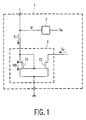
- Fig. 1 shows an integrated circuit which comprises a voltage sensing circuit 2 and a current mirror 3 for sensing both a voltage level Vi and a current Ii at one input terminal T of the integrated circuit.
- the voltage sense circuit 2 has an input connected to the input terminal T and an output supplying a voltage level indication Vu.
- the current mirror 3 has an input connected to the input terminal T, a reference terminal connected to ground potential and an output supplying an output current Iu.
- the current mirror comprises an input transistor T1 with a drain connected to the input terminal T, a source connected to the reference terminal, and a gate connected to the drain of the input transistor T1 and to a gate of an output transistor T2.
- the output transistor T2 has an source connected to the reference terminal and a drain connected to the output of the current mirror.
- the input transistor T 1 has a high impedance as long as the voltage on its drain and gate with respect to the source is lower than the threshold voltage Vth of the input transistor T1. In this case, the current mirror 3 is inactive. Within this voltage range the voltage at the input terminal T can be measured with the voltage sense circuit 2.
- the voltage level indication Vu is a measure of the voltage on the input terminal T.
- the input transistor T1 of the current mirror starts conducting when the voltage on the input terminal reaches the threshold voltage Vth.
- the current mirror 3 becomes active and the output current Iu is a mirrored version of the input current Ii flowing into the input terminal T, because the voltage sensing circuit 2 has a high input impedance.
- the conductive input transistor T1 which is arranged as a diode, stabilizes the input voltage Vi at the input terminal T on the value of the threshold voltage Vth.
- the voltage range in which the current mirror 3 is inactive and thus the voltage sense circuit 2 is able to sense the voltage Vi on the input terminal without being influence by the current mirror 3, can be adapted by selecting the appropriate threshold voltage Vth of the input transistor T1. This is easy if the transistor T3, T2 are field effect transistors as is shown in Fig. 1. It is also possible to connect the sources of the transistors T1 and T2 to a desired reference voltage.
- a current mirror 3 is shown with n-channel field effect transistors T1, T2 and with a reference terminal connected to ground, it is also possible to use p-channel field effect transistors with their sources connected to a supply terminal. Also bipolar transistors can be used.
- Fig. 2 shows a switched mode power supply comprising an integrated circuit 1.
- the integrated circuit 1 comprises a voltage sense circuit 2.
- the voltage sense circuit 2 has a first input connected to an input terminal T of the integrated circuit 1, a second input receiving a reference voltage Vref and an output supplying an output voltage Vu to a first input of a drive circuit 4.
- the integrated circuit 1 further comprises a current mirror 3 which has an input connected to the input terminal T, a reference terminal connected to ground, and an output supplying an output current Iu to a second input of the drive circuit 4.
- the current mirror 3 comprises an input transistor T1 with a collector connected to the input terminal T, an emitter connected to the reference terminal and a base connected to the collector of the input transistor T1 and to a base of an output transistor T2.
- the output transistor T2 has an emitter connected to the reference terminal and a collector connected to the second input the drive circuit 4.
- the drive circuit 4 has an output to supply control pulses Dr to a controllable switching device S which is arranged in series with a primary winding Wp of a transformer Tr.
- the series arrangement of the primary winding Wp and the controllable switching S device receives a DC input voltage Vdc.
- the DC input voltage Vdc may be a rectified mains voltage.
- the control pulses Dr periodically cause the controllable switching device S to have a low impedance and a high impedance.
- a current through the primary winding Wp increases
- the energy in the primary winding Wp is transferred to a secondary winding Ws of the transformer Tr in order to supply power to a load Z.
- a series arrangement of a rectifying diode D2 and an smoothing capacitor C is connected across the secondary winding Ws to supply a rectified voltage Vo to the load Z which is connected in parallel to the smoothing capacitor C.
- Transformer Tr has a further winding Wf which supplies a feedback voltage Vf and which is connected via a resistor R to the terminal T of the integrated circuit 1.
- a diode D1 is connected between the terminal T and the reference terminal to prevent a too large negative voltage across the circuits in the integrated circuit 1. This diode D1 is not relevant to the invention and need not be positioned in the integrated circuit 1.
- the drive circuit 4 comprises a control circuit 41 which receives the output current Iu to supply a drive signal to the controllable switching device S for alternatively switching on and off the controllable switching device S.
- the control circuit 41 controls a duty cycle or frequency of the drive signal in response to the output current Iu for stabilizing the feedback voltage Vf.
- the drive circuit 4 further comprises a demagnetization protection circuit 40 which receives the output voltage Vu to supply a demagnetization protection signal to the control circuit 41 for preventing switch on of the controllable switching device S as long as energy is transferred to the secondary winding Ws.
- a demagnetization protection per se is known from the Motorola Semiconductor technical data "High Flexibility Green SMPS Controller" MC44603.
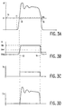
- Fig. 3A shows the feedback voltage Vf supplied by the further winding Wf.
- Fig. 3B shows the input voltage Vi on the input terminal T.
- Fig. 3C shows the output voltage Vu of the voltage sense circuit 2.
- Fig. 3D shows the output current Iu of the current mirror 3.
- the controllable switching device S is conductive, the feedback voltage Vf and the input voltage Vi are negative.
- the input voltage Vi is limited at a value Vneg by a voltage limiting circuit which in this case is the diode D1.
- the controllable switching device S is controlled to become non-conductive, so that the feedback voltage Vf and the input voltage Vi increase in order to become positive.
- the input voltage Vi equals the threshold voltage Vth due to a conductive input transistor T1 of the current mirror 3 as long as the feedback voltage Vf exceeds this threshold voltage Vth.
- the output voltage Vu has a high level during the period t3-t4 that the input voltage Vi is higher than the reference voltage Vref.
- the output voltage Vu is used to obtain the well known demagnetization protection for preventing activation of the controllable switching element S as long as energy is transferred to the secondary winding Ws.
- the output current Iu represents the current flowing through the resistor R in series with the further winding Wg during the period that the feedback voltage Vf is above the threshold voltage Vth.
- the output current Iu is used to stabilize the feedback voltage Vf and the therewith coupled rectified voltage Vo.
- the resistor R may be replaced by a suitable impedance.
- transistors T1 and T2 are p-channel FETs, a value of the reference voltage Vref has to be selected below the threshold voltage Vth occurring at the input terminal T when the current mirror 3 is active.
- the reference terminal to which the emitters of the transistors T1 and T2 are connected may also be connected to a negative or positive reference voltage. In this way it is possible to select a desired threshold voltage Vth for determining when the current mirror 3 is inactive.
- the invention can advantageously be used in an integrated controller IC of a switched mode power supply, whereby only a single terminal of the controller IC is needed to be able to detect a voltage information for the demagnetization protection and a current information to control the controllable switching device to stabilize output voltages.
- the voltage sense circuit 2 and the current mirror 3 according to the invention may also be used in other application where it is important to use one and the same terminal to measure a voltage and a current.
Landscapes
- Engineering & Computer Science (AREA)
- Physics & Mathematics (AREA)
- General Physics & Mathematics (AREA)
- Microelectronics & Electronic Packaging (AREA)
- Nonlinear Science (AREA)
- Electromagnetism (AREA)
- Power Engineering (AREA)
- Radar, Positioning & Navigation (AREA)
- Automation & Control Theory (AREA)
- Dc-Dc Converters (AREA)
- Measurement Of Current Or Voltage (AREA)
- Control Of Electrical Variables (AREA)
- Management, Administration, Business Operations System, And Electronic Commerce (AREA)
- Information Retrieval, Db Structures And Fs Structures Therefor (AREA)
Abstract
Description
Claims (6)
- A circuit for sensing both an input current (Ii) and an input voltage (Vi) at one input terminal (T) of an integrated circuit (1), the integrated circuit (1) comprising a voltage sense circuit (2) having an input coupled to the input terminal (T) to supply a voltage level indication (Vu), and a current mirror (3) having an input coupled to said input terminal (T) for receiving the input current (Ii), and an output for supplying an output current (Iu), the current mirror (3) being active if the input voltage (Vi) exceeds a threshold voltage (Vth), the voltage level indication (Vu) having a value corresponding to the voltage (Vi) at the input terminal (T) when the voltage (Vi) at the input terminal (T) does not exceed the threshold voltage (Vth).
- A circuit for sensing both an input current (Ii) and an input voltage (Vi) at one input terminal (T) as claimed in claim 1, characterized in that the voltage sense circuit (2) comprises a voltage comparator having an input coupled to the input terminal (T) for comparing the voltage (Vi) on the input terminal (T) with a reference value (Vref) to supply the voltage level indication (Vu) for indicating whether the voltage (Vi) on the input terminal (T) falls below or exceeds the reference level (Vref), wherein the reference value (Vref) is selected within a range determined by the threshold voltage (Vth) to compare the voltage (Vi) at the input terminal (T) when the voltage (Vi) at the input terminal (T) does not exceed the threshold voltage (Vth).
- A circuit for sensing both an input current (Ii) and an input voltage (Vi) at one input terminal (T) as claimed in claim 1, characterized in that the current mirror (3) comprises an input transistor (T1) and an output transistor (T2), the input transistor (T1) having a base and a collector being interconnected, and an emitter being coupled to a reference terminal, the base emitter junction providing the threshold voltage (Vth), the output transistor (T2) having a base being coupled to the base of the input transistor (T1), an emitter being coupled to the reference terminal and a collector for supplying the mirrored output current (Iu).
- A power supply comprising:a transformer (Tr) having a primary winding (Wp) and a further winding (Wf), a series arrangement of the primary winding (Wp) and a controllable switching device (S) being coupled to receive a DC input voltage (Vdc),an integrated controller circuit (1) having an output for supplying drive pulses to the controllable switching device (S), the integrated controller circuit (I) having an input terminal (T) being coupled to the further winding (Wf) via an impedance (R), the integrated circuit (1) comprising a voltage sense circuit (2) having an input coupled to the input terminal (T) to supply a voltage level indication (Vu), and a current mirror (3) having an input coupled to said input terminal (T) for receiving the input current (Ii), and an output for supplying an output current (Iu), the current mirror (3) being active if the input voltage (Vi) exceeds a threshold voltage (Vth), the voltage level indication (Vu) having a value corresponding to the voltage (Vi) at the input terminal (T) when the voltage (Vi) at the input terminal (T) does not exceed the threshold voltage (Vth).
- A power supply as claimed in claim 4, characterized in that the integrated controller circuit (1) further comprises a control circuit (41) coupled to receive the output current (Iu) to control the drive pulses for stabilizing a feedback voltage (Vf) supplied by the further winding (Wf).
- A power supply as claimed in claim 5, characterized in that the integrated controller circuit (1) further comprises a demagnetization protection circuit (40) coupled to receive the voltage level indication (Vu) for supplying a demagnetization protection signal to the control circuit (41) for preventing switch on of the controllable switching device (S) as long as energy is transferred from the primary winding (Wp) to the secondary winding Ws.
Priority Applications (1)
| Application Number | Priority Date | Filing Date | Title |
|---|---|---|---|
| EP98903234A EP0904545B1 (en) | 1997-03-21 | 1998-02-27 | Current and voltage sensing |
Applications Claiming Priority (4)
| Application Number | Priority Date | Filing Date | Title |
|---|---|---|---|
| EP97200856 | 1997-03-21 | ||
| EP97200856 | 1997-03-21 | ||
| EP98903234A EP0904545B1 (en) | 1997-03-21 | 1998-02-27 | Current and voltage sensing |
| PCT/IB1998/000249 WO1998043100A2 (en) | 1997-03-21 | 1998-02-27 | Current and voltage sensing |
Publications (2)
| Publication Number | Publication Date |
|---|---|
| EP0904545A2 EP0904545A2 (en) | 1999-03-31 |
| EP0904545B1 true EP0904545B1 (en) | 2004-08-11 |
Family
ID=8228135
Family Applications (1)
| Application Number | Title | Priority Date | Filing Date |
|---|---|---|---|
| EP98903234A Expired - Lifetime EP0904545B1 (en) | 1997-03-21 | 1998-02-27 | Current and voltage sensing |
Country Status (5)
| Country | Link |
|---|---|
| US (1) | US5892355A (en) |
| EP (1) | EP0904545B1 (en) |
| JP (1) | JP4050325B2 (en) |
| DE (1) | DE69825536T2 (en) |
| WO (1) | WO1998043100A2 (en) |
Families Citing this family (22)
| Publication number | Priority date | Publication date | Assignee | Title |
|---|---|---|---|---|
| US6140987A (en) * | 1996-09-18 | 2000-10-31 | Intellinet, Inc. | User interface for home automation system |
| US6344981B1 (en) * | 1999-11-16 | 2002-02-05 | Exabyte Corporation | Power supply circuit and method of calibration therefor |
| US6882552B2 (en) * | 2000-06-02 | 2005-04-19 | Iwatt, Inc. | Power converter driven by power pulse and sense pulse |
| US6894911B2 (en) * | 2000-06-02 | 2005-05-17 | Iwatt, Inc. | Method of driving a power converter by using a power pulse and a sense pulse |
| EP1750137A3 (en) * | 2001-07-20 | 2007-07-11 | Power Integrations, Inc. | Method and apparatus for low cost current and voltage sensing in circuits as a function of a voltage drop |
| US6795321B2 (en) | 2001-07-20 | 2004-09-21 | Power Integrations, Inc. | Method and apparatus for sensing current and voltage in circuits with voltage across an LED |
| WO2003047079A2 (en) * | 2001-11-29 | 2003-06-05 | Iwatt | Power converters with primary-only feedback |
| CN100429690C (en) * | 2002-11-26 | 2008-10-29 | 华邦电子股份有限公司 | Current teading circuit for controlling gain error |
| CN100431251C (en) * | 2003-09-23 | 2008-11-05 | 半导体元件工业有限责任公司 | Negative current compensation method and circuit |
| GB0413494D0 (en) * | 2004-06-16 | 2004-07-21 | Elantec Semiconductor Inc | Non-Leb restricted DC-DC converter |
| EP1635240B1 (en) * | 2004-09-14 | 2010-02-10 | Dialog Semiconductor GmbH | Dynamic transconductance boosting technique for current mirrors |
| CN100395560C (en) * | 2004-10-27 | 2008-06-18 | 华为技术有限公司 | Circuit and method for measuring signal reflow density |
| US7457138B2 (en) * | 2005-07-14 | 2008-11-25 | Semiconductor Components Industries L.L.C. | Single pin multi-function signal detection method and structure therefor |
| US7821245B2 (en) * | 2007-08-06 | 2010-10-26 | Analog Devices, Inc. | Voltage transformation circuit |
| US8432147B2 (en) * | 2008-07-23 | 2013-04-30 | Semiconductor Components Industries, Llc | Method of forming a switching regulator and structure therefor |
| US8391027B2 (en) * | 2008-11-14 | 2013-03-05 | Semiconductor Components Industries, Llc | Quasi-resonant power supply controller and method therefor |
| CN103185826B (en) * | 2011-12-31 | 2016-09-14 | 意法半导体研发(深圳)有限公司 | Bidirectional voltage differentiator circuit |
| US9048752B2 (en) | 2012-09-27 | 2015-06-02 | Semiconductor Components Industries, Llc | Off-line power converter and integrated circuit suitable for use in same |
| CN103956906B (en) * | 2014-04-21 | 2016-07-27 | 华为技术有限公司 | A kind of feedback control circuit |
| US9941803B1 (en) * | 2017-05-16 | 2018-04-10 | Nxp B.V. | Controller IC device for a switched mode power converter and method for operating a controller IC device of a switched mode power converter |
| US10715045B1 (en) | 2019-01-25 | 2020-07-14 | Semiconductor Components Industries, Llc | Methods and systems of operating power converters |
| CN111707962B (en) * | 2020-08-20 | 2020-11-10 | 上海南麟电子股份有限公司 | Alternating current detection circuit |
Family Cites Families (10)
| Publication number | Priority date | Publication date | Assignee | Title |
|---|---|---|---|---|
| DE3330039A1 (en) * | 1983-08-19 | 1985-02-28 | Siemens AG, 1000 Berlin und 8000 München | LOCKING CONVERTER SWITCHING POWER SUPPLY |
| JP2533399B2 (en) * | 1990-05-25 | 1996-09-11 | 三菱電機株式会社 | Sense amplifier |
| US5262713A (en) * | 1991-01-31 | 1993-11-16 | Texas Instruments Incorporated | Current mirror for sensing current |
| JP2761687B2 (en) * | 1991-12-19 | 1998-06-04 | 三菱電機株式会社 | Voltage level detection circuit |
| EP0554936B1 (en) * | 1992-02-03 | 1997-07-09 | Koninklijke Philips Electronics N.V. | Arrangement for turning on and turning off a power transistor |
| US5264782A (en) * | 1992-08-10 | 1993-11-23 | International Business Machines Corporation | Dropout recovery circuit |
| US5313381A (en) * | 1992-09-01 | 1994-05-17 | Power Integrations, Inc. | Three-terminal switched mode power supply integrated circuit |
| US5418674A (en) * | 1993-07-19 | 1995-05-23 | Motorola, Inc. | Multi-lead protected power device having current and boot-strap inputs |
| US5666043A (en) * | 1995-06-07 | 1997-09-09 | Analog Devices, Inc. | Voltage detector with trigger based on output load currency |
| US5680034A (en) * | 1995-09-22 | 1997-10-21 | Toko, Inc. | PWM controller for resonant converters |
-
1997
- 1997-09-29 US US08/939,550 patent/US5892355A/en not_active Expired - Lifetime
-
1998
- 1998-02-27 JP JP52927998A patent/JP4050325B2/en not_active Expired - Fee Related
- 1998-02-27 DE DE69825536T patent/DE69825536T2/en not_active Expired - Lifetime
- 1998-02-27 WO PCT/IB1998/000249 patent/WO1998043100A2/en active IP Right Grant
- 1998-02-27 EP EP98903234A patent/EP0904545B1/en not_active Expired - Lifetime
Also Published As
| Publication number | Publication date |
|---|---|
| DE69825536D1 (en) | 2004-09-16 |
| WO1998043100A2 (en) | 1998-10-01 |
| JP4050325B2 (en) | 2008-02-20 |
| WO1998043100A3 (en) | 1999-01-28 |
| JP2000511285A (en) | 2000-08-29 |
| EP0904545A2 (en) | 1999-03-31 |
| DE69825536T2 (en) | 2005-08-04 |
| US5892355A (en) | 1999-04-06 |
Similar Documents
| Publication | Publication Date | Title |
|---|---|---|
| EP0904545B1 (en) | Current and voltage sensing | |
| US6137696A (en) | Switching regulator for power converter with dual mode feedback input and method thereof | |
| TWI414142B (en) | Power supply control method and system therefor | |
| US5097403A (en) | Current sensing synchronous rectifier apparatus | |
| KR101365100B1 (en) | Low power consumption start-up circuit with dynamic switching | |
| KR100732353B1 (en) | Control module circuit in switching power supply with automatic burst mode operation | |
| KR101020243B1 (en) | Switching mode power supply | |
| US6590789B2 (en) | Method and apparatus for regulating output voltage of a voltage converter | |
| US7019992B1 (en) | Capacitively coupled power supply | |
| JP2876829B2 (en) | Power supply voltage control switching circuit | |
| EP1058176B1 (en) | Power unit, and power supply system | |
| US7733155B2 (en) | Low power voltage detection circuit and method therefor | |
| EP1275195B1 (en) | On chip current source | |
| US5986897A (en) | Switched-mode power supply having a circuit arrangement for turning the switching device when a voltage on the switching device is at a minimum | |
| US5708572A (en) | Switched-mode power supply | |
| US6212082B1 (en) | Device of adjustment of the charge current of a storage capacitor | |
| US6191959B1 (en) | Switched-mode power supply with capacitor controlled power supply | |
| US20080007304A1 (en) | AC-to-DC power circuit | |
| US7154762B2 (en) | Power source apparatus | |
| US6348784B1 (en) | Switching power supply | |
| WO2004057744A1 (en) | Self-oscillating power supply | |
| JPH0974671A (en) | Power source circuit | |
| KR900006659Y1 (en) | Initial operating circuit for switching regulator | |
| JP2000236664A (en) | Switching power supply | |
| KR910007048Y1 (en) | Base driving circuit of main switching tr |
Legal Events
| Date | Code | Title | Description |
|---|---|---|---|
| PUAI | Public reference made under article 153(3) epc to a published international application that has entered the european phase |
Free format text: ORIGINAL CODE: 0009012 |
|
| PUAK | Availability of information related to the publication of the international search report |
Free format text: ORIGINAL CODE: 0009015 |
|
| AK | Designated contracting states |
Kind code of ref document: A2 Designated state(s): DE FR GB |
|
| AK | Designated contracting states |
Kind code of ref document: A3 Designated state(s): DE FR GB |
|
| 17P | Request for examination filed |
Effective date: 19990728 |
|
| GRAP | Despatch of communication of intention to grant a patent |
Free format text: ORIGINAL CODE: EPIDOSNIGR1 |
|
| GRAS | Grant fee paid |
Free format text: ORIGINAL CODE: EPIDOSNIGR3 |
|
| GRAA | (expected) grant |
Free format text: ORIGINAL CODE: 0009210 |
|
| AK | Designated contracting states |
Kind code of ref document: B1 Designated state(s): DE FR GB |
|
| REG | Reference to a national code |
Ref country code: GB Ref legal event code: FG4D |
|
| REF | Corresponds to: |
Ref document number: 69825536 Country of ref document: DE Date of ref document: 20040916 Kind code of ref document: P |
|
| PLBE | No opposition filed within time limit |
Free format text: ORIGINAL CODE: 0009261 |
|
| STAA | Information on the status of an ep patent application or granted ep patent |
Free format text: STATUS: NO OPPOSITION FILED WITHIN TIME LIMIT |
|
| ET | Fr: translation filed | ||
| 26N | No opposition filed |
Effective date: 20050512 |
|
| REG | Reference to a national code |
Ref country code: GB Ref legal event code: 732E |
|
| REG | Reference to a national code |
Ref country code: GB Ref legal event code: 732E |
|
| REG | Reference to a national code |
Ref country code: FR Ref legal event code: TP |
|
| REG | Reference to a national code |
Ref country code: FR Ref legal event code: GC |
|
| REG | Reference to a national code |
Ref country code: GB Ref legal event code: 732E Free format text: REGISTERED BETWEEN 20090618 AND 20090624 |
|
| REG | Reference to a national code |
Ref country code: FR Ref legal event code: GC |
|
| REG | Reference to a national code |
Ref country code: GB Ref legal event code: 732E Free format text: REGISTERED BETWEEN 20101007 AND 20101013 |
|
| REG | Reference to a national code |
Ref country code: FR Ref legal event code: GC |
|
| REG | Reference to a national code |
Ref country code: GB Ref legal event code: 732E Free format text: REGISTERED BETWEEN 20111013 AND 20111019 |
|
| REG | Reference to a national code |
Ref country code: FR Ref legal event code: AU Effective date: 20120126 |
|
| REG | Reference to a national code |
Ref country code: GB Ref legal event code: 732E Free format text: REGISTERED BETWEEN 20120315 AND 20120321 |
|
| REG | Reference to a national code |
Ref country code: GB Ref legal event code: 732E Free format text: REGISTERED BETWEEN 20120705 AND 20120711 |
|
| REG | Reference to a national code |
Ref country code: GB Ref legal event code: 732E Free format text: REGISTERED BETWEEN 20120927 AND 20121003 |
|
| REG | Reference to a national code |
Ref country code: FR Ref legal event code: AU Effective date: 20121009 |
|
| REG | Reference to a national code |
Ref country code: FR Ref legal event code: AU Effective date: 20130402 |
|
| REG | Reference to a national code |
Ref country code: GB Ref legal event code: 732E Free format text: REGISTERED BETWEEN 20130606 AND 20130612 |
|
| REG | Reference to a national code |
Ref country code: DE Ref legal event code: R084 Ref document number: 69825536 Country of ref document: DE |
|
| REG | Reference to a national code |
Ref country code: DE Ref legal event code: R084 Ref document number: 69825536 Country of ref document: DE Effective date: 20141015 |
|
| REG | Reference to a national code |
Ref country code: FR Ref legal event code: PLFP Year of fee payment: 19 |
|
| REG | Reference to a national code |
Ref country code: FR Ref legal event code: PLFP Year of fee payment: 20 |
|
| PGFP | Annual fee paid to national office [announced via postgrant information from national office to epo] |
Ref country code: DE Payment date: 20170119 Year of fee payment: 20 Ref country code: FR Payment date: 20170124 Year of fee payment: 20 |
|
| PGFP | Annual fee paid to national office [announced via postgrant information from national office to epo] |
Ref country code: GB Payment date: 20170124 Year of fee payment: 20 |
|
| REG | Reference to a national code |
Ref country code: DE Ref legal event code: R071 Ref document number: 69825536 Country of ref document: DE |
|
| REG | Reference to a national code |
Ref country code: GB Ref legal event code: PE20 Expiry date: 20180226 |
|
| PG25 | Lapsed in a contracting state [announced via postgrant information from national office to epo] |
Ref country code: GB Free format text: LAPSE BECAUSE OF EXPIRATION OF PROTECTION Effective date: 20180226 |