EP1175130A1 - Electroluminescent element - Google Patents
Electroluminescent element Download PDFInfo
- Publication number
- EP1175130A1 EP1175130A1 EP00904092A EP00904092A EP1175130A1 EP 1175130 A1 EP1175130 A1 EP 1175130A1 EP 00904092 A EP00904092 A EP 00904092A EP 00904092 A EP00904092 A EP 00904092A EP 1175130 A1 EP1175130 A1 EP 1175130A1
- Authority
- EP
- European Patent Office
- Prior art keywords
- anode
- organic layer
- electroluminescent device
- cathode
- group
- Prior art date
- Legal status (The legal status is an assumption and is not a legal conclusion. Google has not performed a legal analysis and makes no representation as to the accuracy of the status listed.)
- Granted
Links
Images


Classifications
-
- C—CHEMISTRY; METALLURGY
- C09—DYES; PAINTS; POLISHES; NATURAL RESINS; ADHESIVES; COMPOSITIONS NOT OTHERWISE PROVIDED FOR; APPLICATIONS OF MATERIALS NOT OTHERWISE PROVIDED FOR
- C09K—MATERIALS FOR MISCELLANEOUS APPLICATIONS, NOT PROVIDED FOR ELSEWHERE
- C09K11/00—Luminescent materials, e.g. electroluminescent or chemiluminescent
- C09K11/06—Luminescent materials, e.g. electroluminescent or chemiluminescent containing organic luminescent materials
-
- H—ELECTRICITY
- H05—ELECTRIC TECHNIQUES NOT OTHERWISE PROVIDED FOR
- H05B—ELECTRIC HEATING; ELECTRIC LIGHT SOURCES NOT OTHERWISE PROVIDED FOR; CIRCUIT ARRANGEMENTS FOR ELECTRIC LIGHT SOURCES, IN GENERAL
- H05B33/00—Electroluminescent light sources
- H05B33/12—Light sources with substantially two-dimensional [2D] radiating surfaces
- H05B33/14—Light sources with substantially two-dimensional [2D] radiating surfaces characterised by the chemical or physical composition or the arrangement of the electroluminescent material, or by the simultaneous addition of the electroluminescent material in or onto the light source
-
- H—ELECTRICITY
- H10—SEMICONDUCTOR DEVICES; ELECTRIC SOLID-STATE DEVICES NOT OTHERWISE PROVIDED FOR
- H10K—ORGANIC ELECTRIC SOLID-STATE DEVICES
- H10K50/00—Organic light-emitting devices
- H10K50/10—OLEDs or polymer light-emitting diodes [PLED]
- H10K50/11—OLEDs or polymer light-emitting diodes [PLED] characterised by the electroluminescent [EL] layers
-
- H—ELECTRICITY
- H10—SEMICONDUCTOR DEVICES; ELECTRIC SOLID-STATE DEVICES NOT OTHERWISE PROVIDED FOR
- H10K—ORGANIC ELECTRIC SOLID-STATE DEVICES
- H10K85/00—Organic materials used in the body or electrodes of devices covered by this subclass
- H10K85/10—Organic polymers or oligomers
- H10K85/111—Organic polymers or oligomers comprising aromatic, heteroaromatic, or aryl chains, e.g. polyaniline, polyphenylene or polyphenylene vinylene
-
- C—CHEMISTRY; METALLURGY
- C09—DYES; PAINTS; POLISHES; NATURAL RESINS; ADHESIVES; COMPOSITIONS NOT OTHERWISE PROVIDED FOR; APPLICATIONS OF MATERIALS NOT OTHERWISE PROVIDED FOR
- C09K—MATERIALS FOR MISCELLANEOUS APPLICATIONS, NOT PROVIDED FOR ELSEWHERE
- C09K2211/00—Chemical nature of organic luminescent or tenebrescent compounds
- C09K2211/14—Macromolecular compounds
- C09K2211/1408—Carbocyclic compounds
- C09K2211/1425—Non-condensed systems
-
- C—CHEMISTRY; METALLURGY
- C09—DYES; PAINTS; POLISHES; NATURAL RESINS; ADHESIVES; COMPOSITIONS NOT OTHERWISE PROVIDED FOR; APPLICATIONS OF MATERIALS NOT OTHERWISE PROVIDED FOR
- C09K—MATERIALS FOR MISCELLANEOUS APPLICATIONS, NOT PROVIDED FOR ELSEWHERE
- C09K2211/00—Chemical nature of organic luminescent or tenebrescent compounds
- C09K2211/14—Macromolecular compounds
- C09K2211/1408—Carbocyclic compounds
- C09K2211/1433—Carbocyclic compounds bridged by heteroatoms, e.g. N, P, Si or B
-
- H—ELECTRICITY
- H10—SEMICONDUCTOR DEVICES; ELECTRIC SOLID-STATE DEVICES NOT OTHERWISE PROVIDED FOR
- H10K—ORGANIC ELECTRIC SOLID-STATE DEVICES
- H10K2102/00—Constructional details relating to the organic devices covered by this subclass
- H10K2102/10—Transparent electrodes, e.g. using graphene
- H10K2102/101—Transparent electrodes, e.g. using graphene comprising transparent conductive oxides [TCO]
- H10K2102/103—Transparent electrodes, e.g. using graphene comprising transparent conductive oxides [TCO] comprising indium oxides, e.g. ITO
-
- Y—GENERAL TAGGING OF NEW TECHNOLOGICAL DEVELOPMENTS; GENERAL TAGGING OF CROSS-SECTIONAL TECHNOLOGIES SPANNING OVER SEVERAL SECTIONS OF THE IPC; TECHNICAL SUBJECTS COVERED BY FORMER USPC CROSS-REFERENCE ART COLLECTIONS [XRACs] AND DIGESTS
- Y10—TECHNICAL SUBJECTS COVERED BY FORMER USPC
- Y10S—TECHNICAL SUBJECTS COVERED BY FORMER USPC CROSS-REFERENCE ART COLLECTIONS [XRACs] AND DIGESTS
- Y10S428/00—Stock material or miscellaneous articles
- Y10S428/917—Electroluminescent
Definitions
- This invention relates to an electroluminescent device comprising at least one electroluminescent organic layer including a light emitting material layer interposed between an anode and a cathode, wherein the light emitting material layer emits light upon application of a voltage between the anode and the cathode.
- An object of the invention is to provide an organic electroluminescent device in which the drive voltage is lowered in order to prevent degradation thereof.
- an electroluminescent device comprising at least one electroluminescent organic layer interposed between the anode and the cathode, especially an electroluminescent device in which an organic hole transporting layer and a light emitting material layer are sequentially deposited on an inorganic electrode (ITO electrode etc.) serving as the anode and the cathode is disposed thereon
- ITO electrode etc. an inorganic electrode
- improved adhesion and an effective lowering of device drive voltage are achieved by providing an auxiliary carrier transporting layer between the anode and the organic layer (especially between the inorganic electrode and the organic hole transporting layer), and forming the auxiliary carrier transporting layer mainly from the aromatic amine derivative of the general formula (1), and especially, the soluble, electrically conductive compound or polymer that the aromatic amine derivative forms with a dopant.
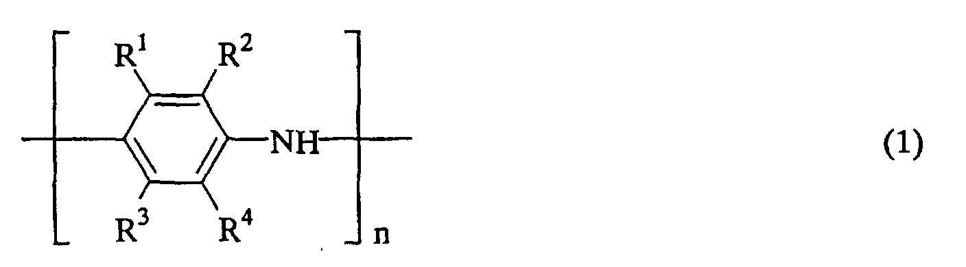
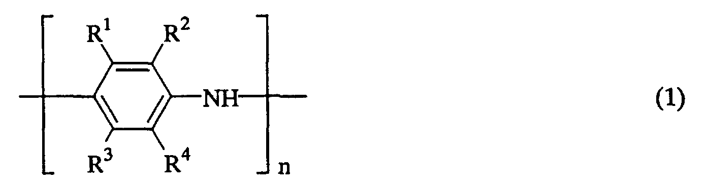
- the invention provides an electroluminescent device comprising an anode, a cathode, and at least one electroluminescent organic layer interposed therebetween, wherein a luminescent material in the organic layer emits light upon application of a voltage between the anode and the cathode, characterized in that an auxiliary carrier transporting layer which contains an aromatic amine derivative comprising recurring units of the following general formula (1) and having a number average molecular weight of 200 to 100,000, and especially a soluble conductive compound in which the aromatic amine derivative forms a salt with an electron accepting dopant, is formed between the anode and the organic layer.
- an auxiliary carrier transporting layer which contains an aromatic amine derivative comprising recurring units of the following general formula (1) and having a number average molecular weight of 200 to 100,000, and especially a soluble conductive compound in which the aromatic amine derivative forms a salt with an electron accepting dopant, is formed between the anode and the organic layer.
- R 1 to R 4 each are independently hydrogen, a hydroxyl group, substituted or unsubstituted monovalent hydrocarbon group, organooxy group, acyl group or sulfonate group, excluding the case where all R 1 to R 4 are hydrogen atoms at the same time, and n is a positive number of 2 to 3,000.
- the electroluminescent device of the invention includes an anode, a cathode and an electroluminescent organic layer therebetween.
- the anode and cathode used herein may be well-known electrodes.
- the anode may be an inorganic electrode (or transparent electrode) of ITO or the like formed on a glass substrate.
- the cathode may be a metallic electrode of aluminum, MgAg alloy or the like.
- the electroluminescent organic layer includes a light emitting material layer and may be of well-known construction.
- a laminate construction in which a hole transporting layer, a light emitting material layer, and a carrier transporting layer are sequentially stacked from the cathode side is typical, though the invention is not limited thereto.
- the hole transporting material is not critical although it is generally selected from tertiary aromatic amines such as N,N,N-tris(p-toluyl)amine (TPD), 1,1-bis[(di-4-toluylamine)phenyl]cyclohexane, N,N'-diphenyl-N',N'-bis(3-methylphenyl)(1,1'-biphenyl)-4,4'-diamine, N,N,N',N'-tetrakis(4-methylphenyl)(1,1'-biphenyl)-4,4'-diamine, N,N'-bis(1-naphthyl)-N,N'-diphenyl-1,1'-bisphenyl-4,4'-diamine, and 4,4',4"-tris(3-methylphenylamino)triphenylamine.
- TPD tertiary aromatic amine
- TPD p-tol
- the carrier transporting material is not critical although generally aromatic fused ring compounds and metal complex compounds are often used.
- metal complex compounds such as tris(8-hydroxyquinoline)aluminum (Alq3) and bis(10-hydroxybenzo[h]quinolate)beryllium (BeBq2), 1,3,4-oxathiazole derivatives, 1,2,4-triazole derivatives, bis(benzimidazole) derivatives of perylene dicarboxyimide, and thiopyrane sulfone derivatives.
- the light emitting material examples include metal complex compounds such as Alq3 and tris(5-cyano-8-hydroxyquinoline)aluminum (Al(Q-CN)), and dyes such as oxathiazoles, e.g., biphenyl-p-(t-butyl)phenyl-1,3,4-oxathiazole, triazoles, allylenes, and coumarins though is not limited thereto.
- metal complex compounds such as Alq3 and tris(5-cyano-8-hydroxyquinoline)aluminum (Al(Q-CN)
- dyes such as oxathiazoles, e.g., biphenyl-p-(t-butyl)phenyl-1,3,4-oxathiazole, triazoles, allylenes, and coumarins though is not limited thereto.
- an auxiliary carrier transporting layer is interposed between the anode and the organic layer, and when the organic layer includes a plurality of layers, between the anode and a layer disposed most closely thereto, typically a hole transporting layer, for assisting in charge transportation.
- the auxiliary carrier transporting layer is primarily composed of an aromatic amine derivative comprising recurring units of the following general formula (1).
- the aromatic amine derivative is used as a thin film of a soluble, electrically conductive compound in which the aromatic amine derivative forms a salt with an electron accepting dopant.
- R 1 to R 4 each are independently hydrogen, a hydroxyl group, substituted or unsubstituted monovalent hydrocarbon group, organooxy group, acyl group or sulfonate group.
- R 1 to R 4 may be the same or different, but R 1 to R 4 are not hydrogen atoms at the same time.
- the substituted or unsubstituted monovalent hydrocarbon groups and organooxy groups represented by R 1 are preferably of 1 to 20 carbon atoms.
- the monovalent hydrocarbon groups include alkyl groups such as methyl, ethyl, propyl, butyl, tert-butyl, hexyl, octyl and decyl; cycloalkyl groups such as cyclopentyl and cyclohexyl; bicycloalkyl groups such as bicyclohexyl; alkenyl groups such as vinyl, 1-propenyl, 2-propenyl, isopropenyl, 1-methyl-2-propenyl, 1-, 2- or 3-butenyl, and hexenyl; aryl groups such as phenyl, xylyl, tolyl, biphenyl and naphthyl; aralkyl groups such as benzyl, phenylethyl and phenylcyclohexyl;
- acyl groups include those of 2 to 10 carbon atoms, for example, acetyl, propionyl, butyryl, isobutyryl and benzoyl.
- R 1 to R 4 are independently selected from among hydrogen atoms, alkyl groups of 1 to 20 carbon atoms, alkoxy groups of 1 to 20 carbon atoms, alkoxyalkyl groups in which the alkoxy moiety has 1 to 20 carbon atoms and the alkyl moiety has 1 to 20 carbon atoms, alkenyl groups of 2 to 4 carbon atoms, acyl groups of 2 to 4 carbon atoms, benzoyl, sulfonate, and hydroxyl, as well as phenyl, cyclohexyl, cyclopentyl, biphenyl, bicyclohexyl and phenylcyclohexyl groups which may have substituents (which are alkyl groups of 1 to 4 carbon atoms or alkoxy groups of 1 to 4 carbon atoms).
- R 1 to R 4 are independently selected from among hydrogen atoms, alkyl groups of 1 to 4 carbon atoms, alkoxy groups of 1 to 4 carbon atoms, alkoxyalkyl groups in which the alkoxy moiety has 1 to 4 carbon atoms and the alkyl moiety has 1 to 4 carbon atoms, vinyl, 2-propenyl, acetyl, benzoyl, sulfonate and hydroxyl, as well as phenyl, cyclohexyl, biphenyl, bicyclohexyl and phenylcyclohexyl groups which may have substituents (which are alkyl groups of 1 to 4 carbon atoms or alkoxy groups of 1 to 4 carbon atoms).
- the alkyl groups of 1 to 4 carbon atoms are methyl, ethyl, propyl, isopropyl, butyl, s-butyl and t-butyl, and the alkoxy groups of 1 to 4 carbon atoms are methoxy, ethoxy, propoxy, isopropoxy, butoxy, s-butoxy and t-butoxy.
- n is a positive number of 2 to 3,000 and preferably 4 to 3,000.
- the aromatic amine derivative of formula (1) has a number average molecular weight of 200 to 100,000 and preferably 400 to 70,000.
- an aniline derivative which is a fully purified starting reactant from which antioxidant and other impurities have been removed as by distillation, is combined with an acid in a 1 to 3-fold amount to form a salt.
- the resulting salt which is soluble in water, is dissolved in water in a 2 to 10-fold amount based on the starting reactant.
- the solution is kept at 25°C, to which ammonium persulfate, cerium sulfate, iron chloride or copper chloride is added as an oxidizing agent.
- the amount of the oxidizing agent added is 0.5 to 4 moles, preferably 1 to 2 moles per mole of the starting reactant.
- reaction is effected for 10 to 50 hours.
- the reaction solution was filtered, the residue was fully washed with a low-boiling, water-soluble organic solvent such as acetone, methanol, ethanol or isopropanol, yielding.
- a soluble conductive compound The acid used herein becomes an electron accepting dopant for the aromatic amine derivative and is not critical.
- the electron accepting dopant is selected from among Lewis acids, protonic acids, transition metal compounds, electrolyte salts and halides.
- Lewis acids include FeCl 3 , PF 5 , AsF 5 , SbF 5 , BF 5 , BCl 3 , and BBr 3 .
- Protonic acids include inorganic acids such as HF, HCl, HNO 5 , H 2 SO 4 and HClO 4 , and organic acids such as benzene sulfonic acid, p-toluenesulfonic acid, dodecylbenzenesulfonic acid, polyvinylsulfonic acid, methanesulfonic acid, 1-butanesulfonic acid, vinylphenylsulfonic acid and camphorsulfonic acid.
- inorganic acids such as HF, HCl, HNO 5 , H 2 SO 4 and HClO 4
- organic acids such as benzene sulfonic acid, p-toluenesulfonic acid, dodecylbenzenesulfonic acid, polyvinylsulfonic acid, methanesulfonic acid, 1-butanesulfonic acid, vinylphenylsulfonic acid and camphorsulfonic acid.
- Transition metal compounds include FeOCl, TiCl 4 , ZrCl 4 , HfCl 4 , NbF 5 , NbCl 5 , TaCl 5 and MoF 5 .
- Electrolyte salts include LiSbF 6 , LiAsF 6 , NaAsF 6 , NaSbF 6 , KAsF 6 , KSbF 6 , [(n-Bu) 4 N]AsF 6 , [(n-Bu) 4 N]SbF 6 , [(n-Et) 4 N]AsF 6 and [(n-Et) 4 N]SbF 6 .
- Halides includes Cl 2 , Br 2 , I 2 , ICl, ICl 3 , IBr and IF.
- ferric chloride is the preferred Lewis acid
- hydrochloric acid is the preferred protonic acid
- perchloric acid is the preferred inorganic acid
- p-toluenesulfonic acid and camphorsulfonic acid are the preferred organic acids.
- the soluble conductive compound obtained by the above method is washed with an alkali, obtaining the desired aromatic amine derivative.
- the alkali used herein is not critical although it is desirably ammonia or sodium hydrogen carbonate.
- the aromatic amine derivative of the invention is readily obtained through alkali treatment of the soluble conductive compound.
- the aromatic amine derivative of the invention thus obtained can be readily converted into a soluble conductive compound or conductive high-molecular-weight compound by doping it with the above-described electron accepting dopant such as a Lewis acid, protonic acid, transition metal compound or electrolyte salt.
- the above-described electron accepting dopant such as a Lewis acid, protonic acid, transition metal compound or electrolyte salt.
- the dopant-forming electron acceptor is generally added in such an amount as to give one or less dopant per nitrogen atom in the recurring units of conjugated structure containing nitrogen as a basic atom.
- doping can be carried out by forming a coating of the aromatic amine derivative of the invention and then exposing the coating to hydrochloric acid vapor or iodine vapor.
- the soluble conductive compounds of the invention are soluble in common organic solvents, for example, chlorinated solvents such as chloroform, dichloroethane, and chlorobenzene, amide solvents such as N,N-dimethylformamide and N,N-dimethylacetamide and polar solvents such as phenolic solvents in a proportion of 2 to 10% by weight.
- chlorinated solvents such as chloroform, dichloroethane, and chlorobenzene
- amide solvents such as N,N-dimethylformamide and N,N-dimethylacetamide
- polar solvents such as phenolic solvents
- polar solvents such as phenolic solvents
- a solvent which does not form a uniform medium when used alone can be used in combination with another solvent insofar as a uniform medium is obtainable.
- Such examples include ethyl cellosolve, butyl cellosolve, ethyl Carbitol, butyl Carbitol, ethyl Carbitol acetate and ethylene glycol.
- additives such as coupling agents to a solution of the soluble conductive compound for the purpose of further improving the adhesion of the soluble conductive compound coating to the substrate.
- the coating method of forming a thin film of the soluble conductive compound includes dipping, spin coating, transfer printing, roll coating and brush coating, but is not limited thereto.
- the coating thickness is not critical although a coating as thin as possible is desirable for improving external emission efficiency. Usually, a thickness of 100 to 1,000 ⁇ is preferred.
- a coating of the aromatic amine derivative or conductive compound thereof according to the invention can be formed on the substrate.
- the temperature used in this step is sufficient for the solvent to evaporate and generally in the range of 80 to 150°C.
- the electroluminescent device of the invention is fabricated by any desired method.
- a thin film of the aromatic amine derivative or conductive compound thereof is first formed on ITO serving as an inorganic electrode.
- the ITO electrode used herein has been removed of foreign matter such as organic matter on the surface by cleaning treatment such as back sputtering, ozone treatment or acid pickling.
- the method of forming a thin film of the aromatic amine derivative or conductive compound thereof is not critical although spin coating or evaporation is preferably used. More preferably, spin coating is used.
- electroluminescent organic materials are deposited on the electrode-bearing substrate thus obtained.
- Their laminate structure largely varies and is not critical. Most often, a device in which a hole transporting layer, a light emitting layer and a carrier transporting layer are sequentially deposited by evaporation is used. These materials are sequentially deposited by vacuum evaporation and on the top of them, a MgAg alloy, for example, is evaporated as a cathode. This results in an electroluminescent device which emits light of a specific wavelength upon application of an electric field.
- the resulting polymer, 2 g was dissolved in 98 g of N,N-dimethylformamide solvent, to which 0.015 mol (3.44 g) of camphorsulfonic acid was added as a dopant, followed by stirring for one day at room temperature.
- the varnish thus obtained was passed through a 0.2-micron filter to remove the insoluble.
- An electroluminescent device was fabricated as follows under such conditions that a thin film was formed from the varnish to a thickness of 100 ⁇ by a spin coating technique.
- ITO-deposited glass was available from Sanyo Electric Co., Ltd. and had an ITO thickness of 1000 ⁇ .
- This substrate was subjected to ultrasonic cleaning with acetone and isopropyl alcohol and then to ozone treatment.
- the varnish was spin coated to form a thin film of 100 ⁇ thick.
- TPD, Alq, and MgAg were formed by vacuum evaporation to a thickness of 400 ⁇ , 600 ⁇ , and 2000 ⁇ , respectively.
- FIG. 1 illustrates the dependence of emission luminance on voltage
- FIG. 2 illustrates the voltage versus current density.
- the resulting polymer, 2 g was dissolved in 98 g of N,N-dimethylformamide solvent, to which 0.03 mol (6.88 g) of camphorsulfonic acid was added as a dopant, followed by stirring for one day at room temperature.
- the varnish thus obtained was passed through a 0.2-micron filter to remove the insoluble.
- Example 1 An electroluminescent device was fabricated as in Example 1.
- ITO-deposited glass was available from Sanyo Electric Co., Ltd. and had an ITO thickness of 1000 ⁇ .
- This substrate was subjected to ultrasonic cleaning with acetone and isopropyl alcohol and then to ozone treatment.
- the varnish was spin coated to form a thin film of 100 ⁇ thick.
- TPD, Alq, and MgAg were formed by vacuum evaporation to a thickness of 400 ⁇ , 600 ⁇ , and 2000 ⁇ , respectively.
- FIG. 3 illustrates the dependence of emission luminance on voltage
- FIG. 4 illustrates the voltage versus current density.
- the resulting polymer, 2 g was dissolved in 98 g of N,N-dimethylformamide solvent, to which 0.015 mol (3.27 g) of 5-sulfosalicylic acid was added as a dopant, followed by stirring for one day at room temperature.
- the varnish thus obtained was passed through a 0.2-micron filter to remove the insoluble.
- varnishes were prepared by adding 0.03 mol of 5-sulfosalicylic acid and 0.045 mol of 5-sulfosalicylic acid, and similarly evaluated.
- ITO-deposited glass was available from Sanyo Electric Co., Ltd. and had an ITO thickness of 1000 ⁇ .
- This substrate was subjected to ultrasonic cleaning with acetone and isopropyl alcohol and then to ozone treatment.
- the varnish was spin coated to form a thin film of 100 ⁇ thick.
- TPD, Alq, and MgAg were formed by vacuum evaporation to a thickness of 400 ⁇ , 600 ⁇ , and 2000 ⁇ , respectively.
- FIG. 3 illustrates the dependence of emission luminance on voltage
- FIG. 4 illustrates the voltage versus current density.
- FIG. 5 illustrates the dependence of emission luminance on voltage
- FIG. 6 illustrates the voltage versus current density.
- Nos. 1 to 5 represent the results of electroluminescent devices of cathode/auxiliary carrier transporting layer/hole transporting layer/light emitting material layer/anode construction
- No. 6 represents the results of an electroluminescent device of cathode/hole transporting layer/light emitting material layer/anode construction.
- the respective layers were composed of the following components.
- the resulting polymer, 2 g was dissolved in 98 g of N,N-dimethylformamide solvent, to which 0.015 mol (3.27 g) of 5-sulfosalicylic acid was added as a dopant, followed by stirring for one day at room temperature. An attempt was made to pass the varnish thus obtained through a 0.2-micron filter to remove the insoluble, but failed. A thin film was formed using the non-filtered varnish, finding asperities in excess of 2000 ⁇ .
- the electroluminescent device of the invention has a low drive voltage.
Landscapes
- Chemical & Material Sciences (AREA)
- Engineering & Computer Science (AREA)
- Materials Engineering (AREA)
- Physics & Mathematics (AREA)
- Optics & Photonics (AREA)
- Organic Chemistry (AREA)
- Electroluminescent Light Sources (AREA)
Abstract

Description

Claims (3)
- An electroluminescent device comprising an anode, a cathode, and at least one electroluminescent organic layer interposed therebetween, wherein a luminescent material in said organic layer emits light upon application of a voltage between the anode and the cathode, characterized in that an auxiliary carrier transporting layer which contains an aromatic amine derivative comprising recurring units of the following general formula (1) and having a number average molecular weight of 200 to 100,000 is formed between said anode and said organic layer,wherein R1 to R4 each are independently hydrogen, a hydroxyl group, substituted or unsubstituted monovalent hydrocarbon group, organooxy group, acyl group or sulfonate group, excluding the case where all R1 to R4 are hydrogen atoms at the same time, and n is a positive number of 2 to 3,000.
- The electroluminescent device of claim 1 wherein said auxiliary carrier transporting layer is formed of a soluble, electrically conductive compound in which said aromatic amine derivative forms a salt with an electron accepting dopant.
- The electroluminescent device of claim 2 wherein the electron accepting dopant is selected from the group consisting of a Lewis acid, protonic acid, transition metal compound, electrolyte salt and halide.
Applications Claiming Priority (3)
| Application Number | Priority Date | Filing Date | Title |
|---|---|---|---|
| JP04407799A JP4375502B2 (en) | 1999-02-23 | 1999-02-23 | Light emitting element |
| JP4407799 | 1999-02-23 | ||
| PCT/JP2000/001000 WO2000051404A1 (en) | 1999-02-23 | 2000-02-22 | Electroluminescent element |
Publications (3)
| Publication Number | Publication Date |
|---|---|
| EP1175130A1 true EP1175130A1 (en) | 2002-01-23 |
| EP1175130A4 EP1175130A4 (en) | 2007-06-27 |
| EP1175130B1 EP1175130B1 (en) | 2018-07-11 |
Family
ID=12681572
Family Applications (1)
| Application Number | Title | Priority Date | Filing Date |
|---|---|---|---|
| EP00904092.4A Expired - Lifetime EP1175130B1 (en) | 1999-02-23 | 2000-02-22 | Electroluminescent element |
Country Status (6)
| Country | Link |
|---|---|
| US (1) | US6632545B1 (en) |
| EP (1) | EP1175130B1 (en) |
| JP (1) | JP4375502B2 (en) |
| KR (1) | KR100536085B1 (en) |
| TW (1) | TW465256B (en) |
| WO (1) | WO2000051404A1 (en) |
Cited By (2)
| Publication number | Priority date | Publication date | Assignee | Title |
|---|---|---|---|---|
| CN1836296B (en) * | 2003-08-14 | 2010-06-09 | 电力研究所有限公司 | Chemically doped synthetic insulators for early detection of potential failures due to exposed fiberglass rods |
| US8207555B2 (en) | 2004-11-05 | 2012-06-26 | Semiconductor Energy Laboratory Co., Ltd. | Light-emitting element and light emitting device using the same |
Families Citing this family (4)
| Publication number | Priority date | Publication date | Assignee | Title |
|---|---|---|---|---|
| JP2002170666A (en) * | 2000-11-29 | 2002-06-14 | Idemitsu Kosan Co Ltd | Organic electroluminescence device and method of manufacturing the same |
| US7956349B2 (en) * | 2001-12-05 | 2011-06-07 | Semiconductor Energy Laboratory Co., Ltd. | Organic semiconductor element |
| WO2003065770A1 (en) * | 2002-01-31 | 2003-08-07 | Sumitomo Chemical Company, Limited | Organic electroluminescence device |
| JP4877874B2 (en) * | 2004-11-05 | 2012-02-15 | 株式会社半導体エネルギー研究所 | LIGHT EMITTING ELEMENT, LIGHT EMITTING DEVICE, ELECTRONIC DEVICE, AND LIGHTING DEVICE |
Family Cites Families (15)
| Publication number | Priority date | Publication date | Assignee | Title |
|---|---|---|---|---|
| US3172862A (en) | 1960-09-29 | 1965-03-09 | Dow Chemical Co | Organic electroluminescent phosphors |
| US3710167A (en) | 1970-07-02 | 1973-01-09 | Rca Corp | Organic electroluminescent cells having a tunnel injection cathode |
| US4356429A (en) | 1980-07-17 | 1982-10-26 | Eastman Kodak Company | Organic electroluminescent cell |
| JPH03216998A (en) * | 1990-01-19 | 1991-09-24 | Ricoh Co Ltd | electroluminescent device |
| EP0443861B2 (en) * | 1990-02-23 | 2008-05-28 | Sumitomo Chemical Company, Limited | Organic electroluminescence device |
| JP2998187B2 (en) | 1990-10-04 | 2000-01-11 | 住友化学工業株式会社 | Organic electroluminescence device |
| JPH0513171A (en) * | 1991-06-28 | 1993-01-22 | Toshiba Corp | Organic thin film electroluminescent device |
| JPH0617046A (en) * | 1992-06-30 | 1994-01-25 | Konica Corp | Organic electroluminescent element |
| US5589108A (en) * | 1993-12-29 | 1996-12-31 | Nitto Chemical Industry Co., Ltd. | Soluble alkoxy-group substituted aminobenzenesulfonic acid aniline conducting polymers |
| US5723873A (en) * | 1994-03-03 | 1998-03-03 | Yang; Yang | Bilayer composite electrodes for diodes |
| US5719467A (en) * | 1995-07-27 | 1998-02-17 | Hewlett-Packard Company | Organic electroluminescent device |
| DE69613093T2 (en) * | 1995-08-21 | 2001-11-22 | Koninklijke Philips Electronics N.V., Eindhoven | ELECTROLUMINESCENT DEVICE |
| KR0176017B1 (en) * | 1996-08-05 | 1999-05-15 | 이서봉 | Water Soluble Conductive Polyaniline Composite |
| US6403236B1 (en) * | 1997-09-04 | 2002-06-11 | Sumitomo Chemical Company, Limited | Polymer light emitting device |
| JP4269113B2 (en) * | 1998-11-10 | 2009-05-27 | 日産化学工業株式会社 | Aromatic amine derivatives and soluble conductive compounds |
-
1999
- 1999-02-23 JP JP04407799A patent/JP4375502B2/en not_active Expired - Lifetime
-
2000
- 2000-02-21 TW TW089102978A patent/TW465256B/en not_active IP Right Cessation
- 2000-02-22 KR KR10-2001-7010777A patent/KR100536085B1/en not_active Expired - Lifetime
- 2000-02-22 EP EP00904092.4A patent/EP1175130B1/en not_active Expired - Lifetime
- 2000-02-22 WO PCT/JP2000/001000 patent/WO2000051404A1/en not_active Ceased
- 2000-02-22 US US09/914,207 patent/US6632545B1/en not_active Expired - Fee Related
Cited By (3)
| Publication number | Priority date | Publication date | Assignee | Title |
|---|---|---|---|---|
| CN1836296B (en) * | 2003-08-14 | 2010-06-09 | 电力研究所有限公司 | Chemically doped synthetic insulators for early detection of potential failures due to exposed fiberglass rods |
| US8207555B2 (en) | 2004-11-05 | 2012-06-26 | Semiconductor Energy Laboratory Co., Ltd. | Light-emitting element and light emitting device using the same |
| US8338196B2 (en) | 2004-11-05 | 2012-12-25 | Semiconductor Energy Laboratory Co., Ltd. | Light-emitting element and light emitting device using the same |
Also Published As
| Publication number | Publication date |
|---|---|
| EP1175130A4 (en) | 2007-06-27 |
| JP4375502B2 (en) | 2009-12-02 |
| US6632545B1 (en) | 2003-10-14 |
| KR20010109298A (en) | 2001-12-08 |
| WO2000051404A1 (en) | 2000-08-31 |
| KR100536085B1 (en) | 2005-12-12 |
| EP1175130B1 (en) | 2018-07-11 |
| JP2000243576A (en) | 2000-09-08 |
| TW465256B (en) | 2001-11-21 |
Similar Documents
| Publication | Publication Date | Title |
|---|---|---|
| JP4868099B2 (en) | Electroluminescent device | |
| US10573821B2 (en) | Phenylcarbazole-based compounds and fluorene-based compounds and organic light emitting device and flat panel display device comprising the same | |
| JP4811573B2 (en) | Charge-transporting organic material containing a compound having a 1,4-dithiine ring | |
| KR100863905B1 (en) | Fluorine-containing compound and organic light emitting device using same | |
| JP4918990B2 (en) | Charge transporting compound, charge transporting material, charge transporting varnish, charge transporting thin film, and organic electroluminescence device | |
| JP3643433B2 (en) | Triphenylamine-containing polyetherketone, process for producing the same, and organic EL device using the same | |
| KR20000011462A (en) | Electroluminescent Assemblies Containing Boron Chelates | |
| EP1477993B1 (en) | Organic conductive material and conductive varnish | |
| US7341678B2 (en) | Charge-transporting varnish | |
| EP1156072B1 (en) | Aromatic amine derivatives, soluble conductive compound, and electroluminescent element | |
| US20010012572A1 (en) | Novel polymer, light-emitting device material and light-emitting device using the same | |
| US7232617B2 (en) | Electroluminescent devices | |
| US6632545B1 (en) | Electroluminescent element | |
| JP4238506B2 (en) | Organic electroluminescence device | |
| US20040126616A1 (en) | Polyester resin, functional device and organic electroluminescent device using polyester resin, and method of manufacturing organic electroluminescent device | |
| JPH08269133A (en) | Novel polymer compound and organic thin film device using the same | |
| JP2005259442A (en) | Organic electroluminescence device | |
| JP2004288531A (en) | Organic electroluminescent element |
Legal Events
| Date | Code | Title | Description |
|---|---|---|---|
| PUAI | Public reference made under article 153(3) epc to a published international application that has entered the european phase |
Free format text: ORIGINAL CODE: 0009012 |
|
| 17P | Request for examination filed |
Effective date: 20010910 |
|
| AK | Designated contracting states |
Kind code of ref document: A1 Designated state(s): AT BE CH CY DE DK ES FI FR GB GR IE IT LI LU MC NL PT SE |
|
| RBV | Designated contracting states (corrected) |
Designated state(s): DE FR GB NL |
|
| A4 | Supplementary search report drawn up and despatched |
Effective date: 20070525 |
|
| 17Q | First examination report despatched |
Effective date: 20071010 |
|
| GRAP | Despatch of communication of intention to grant a patent |
Free format text: ORIGINAL CODE: EPIDOSNIGR1 |
|
| INTG | Intention to grant announced |
Effective date: 20180116 |
|
| GRAS | Grant fee paid |
Free format text: ORIGINAL CODE: EPIDOSNIGR3 |
|
| GRAA | (expected) grant |
Free format text: ORIGINAL CODE: 0009210 |
|
| RIN1 | Information on inventor provided before grant (corrected) |
Inventor name: KIDO, JUNJI Inventor name: ENOMOTO, TOMOYUKI, CHUO KENKYUJO Inventor name: FUKURO, HIROYOSHI, CHUO KENKYUJO Inventor name: FURUSHO, HITOSHI, CHUO KENKYUJO |
|
| RAP1 | Party data changed (applicant data changed or rights of an application transferred) |
Owner name: NISSAN CHEMICAL INDUSTRIES, LTD. Owner name: KIDO, JUNJI |
|
| RBV | Designated contracting states (corrected) |
Designated state(s): DE NL |
|
| RIN1 | Information on inventor provided before grant (corrected) |
Inventor name: FURUSHO, HITOSHI, CHUO KENKYUJO Inventor name: FUKURO, HIROYOSHI, CHUO KENKYUJO Inventor name: KIDO, JUNJI Inventor name: ENOMOTO, TOMOYUKI, CHUO KENKYUJO |
|
| AK | Designated contracting states |
Kind code of ref document: B1 Designated state(s): DE NL |
|
| REG | Reference to a national code |
Ref country code: DE Ref legal event code: R096 Ref document number: 60049830 Country of ref document: DE |
|
| RAP2 | Party data changed (patent owner data changed or rights of a patent transferred) |
Owner name: KIDO, JUNJI Owner name: NISSAN CHEMICAL CORPORATION |
|
| REG | Reference to a national code |
Ref country code: NL Ref legal event code: FP |
|
| RIC2 | Information provided on ipc code assigned after grant |
Ipc: H05B 33/14 20060101ALI20000904BHEP Ipc: H05B 33/22 20060101AFI20000904BHEP |
|
| REG | Reference to a national code |
Ref country code: DE Ref legal event code: R097 Ref document number: 60049830 Country of ref document: DE |
|
| PGFP | Annual fee paid to national office [announced via postgrant information from national office to epo] |
Ref country code: NL Payment date: 20190123 Year of fee payment: 20 Ref country code: DE Payment date: 20190124 Year of fee payment: 20 |
|
| PLBE | No opposition filed within time limit |
Free format text: ORIGINAL CODE: 0009261 |
|
| STAA | Information on the status of an ep patent application or granted ep patent |
Free format text: STATUS: NO OPPOSITION FILED WITHIN TIME LIMIT |
|
| 26N | No opposition filed |
Effective date: 20190412 |
|
| REG | Reference to a national code |
Ref country code: DE Ref legal event code: R071 Ref document number: 60049830 Country of ref document: DE |
|
| REG | Reference to a national code |
Ref country code: NL Ref legal event code: MK Effective date: 20200221 |