EP1175084A2 - Semiconductor image pickup device - Google Patents
Semiconductor image pickup device Download PDFInfo
- Publication number
- EP1175084A2 EP1175084A2 EP01105550A EP01105550A EP1175084A2 EP 1175084 A2 EP1175084 A2 EP 1175084A2 EP 01105550 A EP01105550 A EP 01105550A EP 01105550 A EP01105550 A EP 01105550A EP 1175084 A2 EP1175084 A2 EP 1175084A2
- Authority
- EP
- European Patent Office
- Prior art keywords
- power supply
- supply voltage
- column direction
- row
- transistor
- Prior art date
- Legal status (The legal status is an assumption and is not a legal conclusion. Google has not performed a legal analysis and makes no representation as to the accuracy of the status listed.)
- Granted
Links
Images




Classifications
-
- H—ELECTRICITY
- H04—ELECTRIC COMMUNICATION TECHNIQUE
- H04N—PICTORIAL COMMUNICATION, e.g. TELEVISION
- H04N25/00—Circuitry of solid-state image sensors [SSIS]; Control thereof
- H04N25/70—SSIS architectures; Circuits associated therewith
- H04N25/76—Addressed sensors, e.g. MOS or CMOS sensors
-
- H—ELECTRICITY
- H04—ELECTRIC COMMUNICATION TECHNIQUE
- H04N—PICTORIAL COMMUNICATION, e.g. TELEVISION
- H04N25/00—Circuitry of solid-state image sensors [SSIS]; Control thereof
- H04N25/40—Extracting pixel data from image sensors by controlling scanning circuits, e.g. by modifying the number of pixels sampled or to be sampled
-
- H—ELECTRICITY
- H04—ELECTRIC COMMUNICATION TECHNIQUE
- H04N—PICTORIAL COMMUNICATION, e.g. TELEVISION
- H04N25/00—Circuitry of solid-state image sensors [SSIS]; Control thereof
- H04N25/60—Noise processing, e.g. detecting, correcting, reducing or removing noise
- H04N25/67—Noise processing, e.g. detecting, correcting, reducing or removing noise applied to fixed-pattern noise, e.g. non-uniformity of response
- H04N25/671—Noise processing, e.g. detecting, correcting, reducing or removing noise applied to fixed-pattern noise, e.g. non-uniformity of response for non-uniformity detection or correction
- H04N25/673—Noise processing, e.g. detecting, correcting, reducing or removing noise applied to fixed-pattern noise, e.g. non-uniformity of response for non-uniformity detection or correction by using reference sources
-
- H—ELECTRICITY
- H04—ELECTRIC COMMUNICATION TECHNIQUE
- H04N—PICTORIAL COMMUNICATION, e.g. TELEVISION
- H04N25/00—Circuitry of solid-state image sensors [SSIS]; Control thereof
- H04N25/70—SSIS architectures; Circuits associated therewith
- H04N25/76—Addressed sensors, e.g. MOS or CMOS sensors
- H04N25/77—Pixel circuitry, e.g. memories, A/D converters, pixel amplifiers, shared circuits or shared components
Definitions
- the present invention relates to a semiconductor image pickup device provided with an image pickup pixel array. More specifically, this invention relates to a semiconductor image pickup device which sequentially selects pixels based on the X-Y address method and reads the output signal.
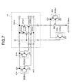
- Fig. 7 is a schematic block diagram of a conventional semiconductor image pickup device of X-Y address type.
- This semiconductor image pickup device comprises a pixel array 51 having a plurality of pixels arranged in a matrix, column direction read transistors (a column direction read transistor 58n and the like), column direction reset signal buffers (a column direction reset signal buffer 59n and the like) , column direction read control line buffers (a column direction read control line buffer 60n and the like) provided for the respective columns of the pixel array 51, and row direction reset signal buffers (a row direction reset signal buffer 61m and the like) and row direction read control line buffers (a row direction read control line buffer 62m and the like) provided for the respective rows of the pixel arrays 51.
- Each pixel on the pixel array 51 e.g., a pixel 52mn in row m and column n (the row m and the column n is an arbitrary matrix number of the pixel array 51) comprises a light receiving element (photodiode) 53mn, a column direction reset transistor 54mn, a row direction reset transistor 55mn, an amplification AMI (Amplified MOS Imager) transistor 56mn and a row direction read transistor 57mn.
- the column direction reset transistor 54mn is connected to the charge accumulation section of the photodiode 53mn.
- the column direction reset signal buffer 59n receives a column direction reset signal XR2 [n] and turns on or off the respective column direction reset transistors (the column direction reset transistor 54mn and the like) in column n depending upon the received signal.
- the column direction read signal buffer 60n receives a column direction read signal XS2 [n] and turns on or off the column direction read transistor 58n depending upon the received signal.
- the row direction reset signal buffer 61m receives a column direction reset signal YR2[m] and turns on or off the respective row direction reset transistors (the row direction reset transistor 55mn and the like) in row m depending upon the received signal.
- the row direction read signal buffer 62m receives a column direction read signal YS2 [m] and turns on or off the respective row direction read transistors (the row direction read transistor 57mn and the like) in row m depending upon the received signal.
- both the column direction reset transistor 54mn and the row direction reset transistor 55mn are turned on, the voltage of the anode of the photodiode 53mn becomes a photodiode reset power voltage VDC, charges accumulated in the photodiode 53mn are discharged and the photodiode 53mn is turned into a reset state. That is, the pixel 52mn is reset. If both the column direction read transistor 58n and the row direction read transistor 57mn are turned on, a current according to the charges accumulated in the photodiode 53mn flows into the amplification AMI transistor 56mn and is outputted as an output signal. That is, read operation is carried out.
- the same power is supplied to the respective pixels (the pixel 52mn and the like) , the column direction reset signal buffers (the column direction reset signal buffer 59n and the like), the column direction read signal buffers (the column direction read signal buffer 60n and the like) , the row direction reset signal buffers (the row direction reset signal buffer 61m and the like) and the row direction read signal buffers (the row direction read signal buffer 62m and the like).
- Fig. 8 is an explanatory view for the operation of the conventional semiconductor image pickup device.
- two pixels on the pixel array 51 are simultaneously read and reset.
- a pixel 52qs in row q and column s is reset
- a pixel 52pr in row p and column r is simultaneously read.
- the positions of the pixels to be reset and read move from a row q, column s position and a row p, column r position to a row q, column (s+1) position and a row p, column (r+1) position, respectively.
- reset and read target rows move to rows (q+1) and (p+1).
- the reset or read position returns to the leading row and column. In this way, scanning is carried out.
- Fig. 9 is a timing chart showing the operation of the conventional semiconductor image pickup device.
- the row direction reset signal YR2[m] is kept to be turned on (high level) until the reset of the row m is completed.
- the column direction reset signal XR2[n] is turned on (A2 in Fig. 9)
- the pixel 52mn is reset.
- the row direction read signal YS2[m] is kept to be turned on until the read of the row m is completed.
- the column direction read signal XS2[n] is turned on (B2 in Fig. 9)
- the pixel 52mn is read.
- the row direction reset signal YR2 [m] is turned off after the reset selected row is moved to row (m+1) but the column direction reset signal XR2 [n] is turned on and off a plurality of times (C2 in Fig. 9). This is because pixels in rows other than the row m and in column n are reset.
- the number of times at which the column direction reset signal XR2[n] is turned on and off corresponds to the positional relationship between a reset target row and a read target row. In case of Fig. 8, for example, the column direction reset signal XR2[n] is turned on and off (q-p-1) times.
- Fig. 10A to Fig. 10C are explanatory views for the charge-pumping operation (charge-pumping phenomenon) of the conventional semiconductor image pickup device.
- the row direction reset signal YR2 [m] and the column direction reset signal XR2 [n] are turned off (low level) , a power supply voltage is applied to the gate control signal line 77 of the column direction reset transistor 54mn by the column direction reset signal buffer 59n, and the column direction reset transistor 54mn is turned off.
- the row direction reset signal YR2[m] is kept to be turned off and a current between the p+ source layer 71 and p+ drain layer 72 of the column direction reset transistor 54mn is cut off (see Fig. 10A).
- the gate control signal line 77 is grounded and the charges (electrons in this example) accumulated in the parasitic capacity between the gate 76 and the p-type silicon substrate 75 of the column direction reset transistor 54mn are discharged to an n-well layer 74 side (see Fig. 10B).
- a power supply voltage is applied again to the gate control signal line 77 and charges are accumulated again in the parasitic capacity between the gate 76 and the p-type silicon substrate 75.
- part of charges flow into the charge accumulation section (p-charge accumulation layer) 73 of the photodiode 53mn (see Fig. 10C).
- the potential of the p-charge accumulation layer 73 changes.
- Fig. 11 shows how the quantity of accumulated charges of the photodiode 53mn changes with the passage of time in case of the conventional semiconductor image pickup device.
- the photodiode 53mn has a change in charge accumulation quantity due to the charge-pumping operation. That is, in addition to the charge accumulation by the optical signal from the outside, the charge accumulation by the charge pump operation is carried out.
- the quantity potential variation of the photodiode due to this charge pumping operation is susceptible to process irregularities such as the finished dimensions of the gate of the column direction reset transistor. Due to this, the potential variation differs among the pixels, which is one cause for fixed pattern noise.
- the column direction reset signal buffers control switching gates (column direction reset transistors) connected to the charge accumulation section of light receiving elements, respectively, while using the power voltage common to the pixel array 51. For that reason, the quantity of charges to be charged and discharged in the charge pumping operation increases, thereby disadvantageously increasing fixed pattern noise.
- the semiconductor image pickup device comprises a switching gate control unit for controlling the switching gate using a lower control power supply voltage than a power supply voltage of the pixel array.
- This switching gate control unit controls the switching gate connected to the charge accumulation section of the light receiving element using a lower control power supply voltage than the power supply voltage of the pixel array.
- control power supply voltage is set to be lower than the power supply voltage of the pixel array and to be not lower than a voltage obtained by subtracting the threshold voltage of the transistor in the switching gate control unit turned on if the switching gate is cut off, from the power supply voltage of the pixel array. Because of such arrangement, it is possible to suppress leak current flowing from the light receiving element through the transistor.
- control power supply voltage generation unit is provided for generating the control power supply voltage. Accordingly, it is not necessary to input a control power supply voltage from an external circuit.
- control power supply voltage generation unit is a resistance division circuit dividing the power supply voltage of the pixel array by a plurality of resistors and generating the control power supply voltage. -Thus, power consumption can be reduced.
- Fig. 1 is a schematic block diagram of a semiconductor image pickup device of X-Y address type according to the first embodiment of the present invention.
- This semiconductor image pickup device comprises a pixel array 1 having a plurality of pixels arranged in a matrix, as well as column direction read transistors (a column direction read transistor 8n and the like), column direction reset signal buffers (a column direction reset signal buffer 9n and the like) and column direction read control line buffers (a column direction read control line buffer 10n and the like) provided for the respective columns of the pixel array 1.
- column direction read transistors a column direction read transistor 8n and the like
- column direction reset signal buffers a column direction reset signal buffer 9n and the like
- column direction read control line buffers a column direction read control line buffer 10n and the like
- the semiconductor device also comprises row direction reset signal buffers (a row direction reset signal buffer 11m and the like) and row direction read control line buffers (a row direction read control line buffer 12m and the like) provided for the respective rows of the pixel array 1, as well as resistors 13 and 14 provided in series between the power supply of the pixel array 1 and a ground and an operational amplifier 15 provided between the middle point of the resistors 13 and 14 and the column direction reset signal buffers.
- row direction reset signal buffers a row direction reset signal buffer 11m and the like
- row direction read control line buffers a row direction read control line buffer 12m and the like
- Each pixel of the pixel array e.g., a pixel 2mn in row m and column n (where the row m and column n is an arbitrary matrix number of the pixel array 1) comprises a light receiving element (photodiode) 3mn, a column direction reset transistor 4mn, a row direction reset transistor 5mn, an amplification AMI (Amplified MOS Imager) transistor 6mn and a row direction read transistor 7mn.
- the resistors 13, 14 and the operational amplifier 15 constitute a circuit for generating a control power supply voltage which value is lower than that of the power supply voltage of the pixel array 1.
- the circuit supplies this control power supply voltage to the respective column direction reset buffers. Namely, using two divided resistors 13 and 14, an intermediate potential (a control power supply voltage) is generated.
- the value of the control power supply voltage is VDD ⁇ R2 (R1+R2) while assuming that the power supply voltage value of the pixel array 1 is VDD, the resistance value of the resistor 13 is R2 and the resistance value of the resistor 14 is R1.
- This circuit employs the operational amplifier 15. Due to this, even if the number of pixels increases and the parasitic capacity of signal lines increases, it is possible to ensure stable operation. Further, by setting the resistance values of the resistors 13 and 14 at maximum values or values close to the maximum values in a range in which the parasitic capacity of the signal lines can be charged and discharged and in which the charge accumulation section of the photodiode can be reset, power consumption can be minimized.
- the photodiode 3mn which has a cathode connected to the power supply of the pixel array 1, converts an optical signal from an external unit into an electric signal and accumulates charges according to the optical signal in the charge accumulation section.
- the column direction reset transistor 4mn is a p-type MOS transistor and has a source connected to the anode of the photodiode 3mn.
- the row direction reset transistor 5mn is a p-type MOS transistor and has a source connected to the drain of the column direction reset transistor 4mn and a drain connected to a photodiode reset power supply (voltage VDC).
- the amplification AMI (Amplified MOS Imager) transistor 6mn is a p-type MOS transistor.
- the transistor 6mn has a gate connected to the anode of the photodiode 3mn and a source connected to the power supply of the pixel array 1, and flows a current according to the charges accumulated in the photodiode 3mn.
- the row direction read transistor 7mn is a p-type MOS transistor and has a source connected to the drain of the amplification AMI transistor 6mn.
- the column direction read transistor 8n is a p-type MOS transistor.
- the transistor 8n has a source connected to the drain of the respective row direction read transistors in column n and outputs an output signal from the drain. While this embodiment shows a case where the transistors of the respective pixels are p-type transistors, they may be n-type transistors, or some may be p-type transistors and others may be n-type transistors.
- the column direction reset signal buffer 9n is constituted by a CMOS circuit.
- the buffer 9n receives a column direction reset signal XR1[n] from the gates of a p-type MOS transistor 16 and of an n-type MOS transistor in this CMOS circuit.
- the buffer 9n uses the control power supply voltage from the operational amplifier 15, the buffer 9n turns on and off the respective column direction reset transistors (the column direction reset transistor 4mn and the like) in column n.
- the p-type MOS transistor 16 is turned on.
- the resistance values of the resistors 13 and 14 are set so that the control power supply voltage has a higher voltage value than a value obtained by subtracting the threshold voltage of the p-type MOS transistor 16 from the power supply voltage of the pixel array 1. By so setting, it is possible to prevent leak current flowing from the photodiodes of the respective column direction reset transistors through the p-type MOS transistor 16.
- the column direction read signal buffer 10n is constituted by a CMOS circuit. The buffer 10n receives a column direction read signal XS1[n] from the gate of the p-type MOS transistor and that of the n-type MOS transistor in the CMOS circuit and turns on and off the column direction read transistor 8n using the power supply voltage of the pixel array 1.
- the row direction reset signal buffer 11m is constituted by a CMOS circuit.
- the buffer 11m receives a row direction reset signal YR1[m] from the gate of a p-type MOS transistor and that of an n-type MOS transistor in this CMOS circuit, and turns on and off the respective row direction reset transistors (the row direction reset transistor 5mn and the like) in row m using the power supply voltage of the pixel array 1.
- the row direction read signal buffer 12m is constituted by a CMOS circuit.
- the buffer 12m receives a column direction read signal YS1[m] from the gates of a p-type MOS transistor and an n-type MOS transistor in this CMOS circuit and turns on and off the respective row direction read transistors (the row direction read transistor 7mn and the like) using the power supply voltage of the pixel array 1.
- the buffers 10n, 11m and 12m may have different voltage values from that of the pixel array 1.
- the rows and the columns may be replaced in this embodiment.
- the column direction reset transistor 4mn corresponds to the switching gate of the present invention
- the column direction reset signal buffer 9n corresponds to the switching gate control unit of the present invention
- the circuit consisting of the resistors 13, 14 and the operational amplifier 15 corresponds to the control power supply voltage generation unit of the present invention.
- FIG. 2 is an explanatory view for the operation of the semiconductor image pickup device in the first embodiment.
- two pixels are simultaneously read and reset on the pixel array 1.
- a pixel 2qs in row q and column s is reset
- a pixel 2pr in row p and column r is simultaneously read.
- the positions of the pixels to be reset and read move from a row q, column s position and a row p, column r position to a row q, column (s+1) position and a row p, column (r+1) position, respectively.
- reset and read target rows move to rows (q+1) and (p+1).
- the reset or read position After completing with the last row and column, the reset or read position returns to a leading row and column. In this way, scanning is carried out.
- Fig. 3 is a timing chart showing the operation of the semiconductor image pickup device in the first embodiment.
- the row direction reset signal YR1[m] is kept to be turned on (high level) until the reset of the row m is completed.
- the column direction reset signal XR1[n] is turned on (A1 in Fig. 3)
- the pixel 2mn is reset.
- the row direction read signal YS1[m] is kept to be turned on until the read of the row m is completed.
- the column direction read signal XS1[n] is turned on (B1 in Fig. 3)
- the pixel 2mn is read.
- the row direction reset signal YR1 [m] is turned off after the reset selected row is moved to row (m+1) but the column direction reset signal XR1 [n] is turned on and off a plurality of times (C1 in Fig. 3). This is because pixels in rows other than the row m and in column n are reset.
- the number of times at which the column direction reset signal XR1[n] is turned on and off corresponds to the positional relationship between a reset target row and a read target row. In case of Fig. 2, for example, the column direction reset signal XR1[n] is turned on and off (q-p-1) times.
- Fig. 4 is an explanatory view for the charge-pumping operation (charge pumping phenomenon) of the semiconductor image pickup device in the first embodiment.
- the row direction reset signal YR1[m] and the column direction reset signal XR1[n] are turned off (low level)
- a control power supply voltage is applied to the gate control signal line 27 of the column direction reset transistor 4mn by the column direction reset signal buffer 9n, and the column direction reset transistor 4mn is turned off.
- the row direction reset signal YR1 [m] is kept to be turned off and a current is cut off between the p+ source layer 21 and p+ drain layer 22 of the column direction reset transistor 4mn (see Fig. 4A).
- the gate control signal line 7 When the column direction reset signal XR1 [n] is turned on, the gate control signal line 7 is grounded and charges (electrons in this case) accumulated in the parasitic capacity between the gate 26 and the p-type silicon substrate 25 of the column direction reset transistor 4mn are discharged to an n-well layer 24 side (see Fig. 4B). Thereafter, when the column direction reset signal XR1[n] is turned off, a control power supply voltage is applied again to the gate control signal line 7 and charges are accumulated again in the parasitic capacity between the gate 26 and the silicon substrate 25.
- this semiconductor image pickup device if the column direction reset transistor 4mn is cut off, a voltage applied to the gate 26 is a control power supply voltage lower than the power supply voltage of the pixel array 1. Due to this, charges flowing into the charge accumulation section (p charge accumulation layer) 23 of the photodiode 3mn in the charge and discharge process are reduced (see Fig. 4C). In this way, this semiconductor image pickup device is capable of suppressing the charge-pumping operation and reducing fixed pattern noise.
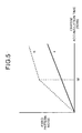
- Fig. 5 shows the fixed pattern noise of the semiconductor image pickup device in the first embodiment.
- the fixed pattern noise of this semiconductor image pickup device is reduced compared with that of the above-stated conventional device. That is, if the charge accumulation time is shorter than a time in which the scanning of the number of rows M on the pixel array 1 are completed, the reduced amount of the fixed pattern increases proportionately to the charge accumulation time (or by how many rows a reset target row and a read target row are distant from each other).
- the respective column direction reset signal buffers (the column direction reset signal buffer 9n and the like) control the corresponding column direction reset transistors (the column direction reset transistor 4mn and the like) using the control power supply voltage lower than the power supply voltage of the pixel array 1.
- the quantity of charges in the charge pumping operation decreases, thereby making it possible to reduce fixed pattern noise.
- control power supply voltage is set to be lower than the power supply voltage of the pixel array 1 and to be not lower than a voltage value obtained by subtracting the threshold voltages of the transistors (the p-type MOS transistor 16 and the like) to be turned on, of the respective column direction reset signal buffers from the power supply voltage of the pixel array 1.
- the control power supply voltage generation circuit consisting of the resistors 13, 14 and the operational amplifier 15 is provided on the semiconductor image pickup device.
- a control power supply voltage generation circuit only consisting of a resistance division circuit is provided instead of the control power supply voltage consisting of the resistors 13, 14 and the operational amplifier 15 as shown in the first embodiment described above. Since the basic constitution and operation of the semiconductor image pickup device in this embodiment are the same as those in the first embodiment, only different parts will be described herein.
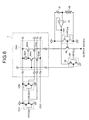
- Fig. 6 is a schematic block diagram of the semiconductor image pickup device in the second embodiment. It is noted that the same constituent elements as those in the first embodiment are denoted by the same legends.
- this semiconductor image pickup device comprises resistors 31 and 32 provided in series between the power supply of a pixel array 1 and a ground instead of the resistors 13, 14 and the operational amplifier 15 provided in the semiconductor image pickup device in the first embodiment.
- the middle point of a resistance division circuit consisting of the resistors 31 and 32 is connected to respective column direction reset signal buffers (a column direction reset signal buffer 9n and the like).
- the resistance division circuit supplies an intermediate potential (a control power supply voltage) to the respective column direction reset signal buffers.
- the remaining constituent elements and operation are the same as those in the first embodiment.
- the resistance division circuit consisting of the resistors 31 and 32 generate a power supply voltage for the respective column direction reset signal buffers (the column direction reset signal buffer 9n and the like) without using an operational amplifier. This can reduce the number of parts, cost and the power consumption corresponding to the power consumed by the operational amplifier.
- the switching gate control unit controls the switching gate connected to the charge accumulation section of the light receiving element using a lower control power supply voltage than the power supply voltage of the pixel array.
- control power supply voltage is set to be lower than the power supply voltage of the pixel array and to be not lower than a voltage obtained by subtracting the threshold voltage of the transistor in the switching gate control unit turned on if the switching gate is cut off, from the power supply voltage of the pixel array.
- control power supply voltage generation unit generates the control power supply voltage.
- it is not necessary to input a control power supply voltage from an external circuit. This can advantageously facilitate the design of external circuits and reduce cost.
- control power supply voltage generation unit is constituted by the resistance division circuit without using an operational amplifier.
- power consumption can be advantageously reduced.
Landscapes
- Engineering & Computer Science (AREA)
- Multimedia (AREA)
- Signal Processing (AREA)
- Transforming Light Signals Into Electric Signals (AREA)
- Solid State Image Pick-Up Elements (AREA)
Abstract
Description
Claims (4)
- A semiconductor image pickup device comprising:a pixel array (1) having a plurality of pixels arranged in a matrix form, each pixel having a light receiving element (3mn) for converting an optical signal into an electric signal and a switching gate (4mn) connected to a charge accumulation section of said light receiving element (3mn); anda switching gate control unit (9n) which controls said switching gate (4mn) using a lower control power supply voltage than a power supply voltage of said pixel array (1).
- The semiconductor image pickup device according to claim 1, wherein the control power supply voltage is not lower than a voltage obtained by subtracting a threshold voltage of a transistor in said switching gate control unit (4mn) turned on if said switching gate (4mn) is cut off, from the power supply voltage of said pixel array (1).
- The semiconductor image pickup device according to claim 1 or 2, further comprising a control power supply voltage generation unit (13, 14, 15) for generating the control power supply voltage.
- The semiconductor image pickup device according to claim 3, wherein the control power supply voltage generation unit (13, 14, 15) is a resistance division circuit dividing the power supply voltage of said pixel array (1) by a plurality of resistors and generating the control power supply voltage.
Applications Claiming Priority (2)
| Application Number | Priority Date | Filing Date | Title |
|---|---|---|---|
| JP2000221309 | 2000-07-21 | ||
| JP2000221309A JP2002044523A (en) | 2000-07-21 | 2000-07-21 | Semiconductor imaging device |
Publications (3)
| Publication Number | Publication Date |
|---|---|
| EP1175084A2 true EP1175084A2 (en) | 2002-01-23 |
| EP1175084A3 EP1175084A3 (en) | 2002-06-19 |
| EP1175084B1 EP1175084B1 (en) | 2004-08-04 |
Family
ID=18715743
Family Applications (1)
| Application Number | Title | Priority Date | Filing Date |
|---|---|---|---|
| EP01105550A Expired - Lifetime EP1175084B1 (en) | 2000-07-21 | 2001-03-06 | Semiconductor image pickup device |
Country Status (5)
| Country | Link |
|---|---|
| US (1) | US6518559B2 (en) |
| EP (1) | EP1175084B1 (en) |
| JP (1) | JP2002044523A (en) |
| CN (1) | CN1185865C (en) |
| DE (1) | DE60104611T2 (en) |
Families Citing this family (7)
| Publication number | Priority date | Publication date | Assignee | Title |
|---|---|---|---|---|
| US7268924B2 (en) * | 2001-01-22 | 2007-09-11 | Hand Held Products, Inc. | Optical reader having reduced parameter determination delay |
| WO2002063543A2 (en) | 2001-01-22 | 2002-08-15 | Hand Held Products, Inc. | Optical reader having partial frame operating mode |
| US7408195B2 (en) * | 2003-09-04 | 2008-08-05 | Cypress Semiconductor Corporation (Belgium) Bvba | Semiconductor pixel arrays with reduced sensitivity to defects |
| WO2005036720A2 (en) * | 2003-10-02 | 2005-04-21 | Digirad Corporation | Charge pump power supply with noise control |
| JP4307322B2 (en) * | 2004-05-18 | 2009-08-05 | キヤノン株式会社 | Radiation imaging apparatus and radiation imaging system |
| US20070001103A1 (en) * | 2005-07-01 | 2007-01-04 | Labelle John | Apparatus and methods for reducing noise in an optoelectronic device |
| JP2008199254A (en) * | 2007-02-13 | 2008-08-28 | Matsushita Electric Ind Co Ltd | Solid-state imaging device, driving method thereof, and imaging device |
Family Cites Families (9)
| Publication number | Priority date | Publication date | Assignee | Title |
|---|---|---|---|---|
| US4484223A (en) * | 1980-06-12 | 1984-11-20 | Canon Kabushiki Kaisha | Image sensor |
| EP0120977B1 (en) * | 1982-10-11 | 1992-04-08 | Fujitsu Limited | Card image data processing system |
| US4839735A (en) * | 1986-12-22 | 1989-06-13 | Hamamatsu Photonics K.K. | Solid state image sensor having variable charge accumulation time period |
| US5083175A (en) * | 1990-09-21 | 1992-01-21 | Xerox Corporation | Method of using offset gated gap-cell thin film device as a photosensor |
| JPH06339082A (en) * | 1993-05-28 | 1994-12-06 | Canon Inc | Photoelectric conversion device |
| TW421962B (en) | 1997-09-29 | 2001-02-11 | Canon Kk | Image sensing device using mos type image sensing elements |
| EP0928101A3 (en) | 1997-12-31 | 2001-05-02 | Texas Instruments Incorporated | CMOS area array sensors |
| JP3581031B2 (en) * | 1998-11-27 | 2004-10-27 | オリンパス株式会社 | Photodetector |
| US6215113B1 (en) * | 1999-04-22 | 2001-04-10 | National Science Council | CMOS active pixel sensor |
-
2000
- 2000-07-21 JP JP2000221309A patent/JP2002044523A/en active Pending
- 2000-12-08 US US09/731,802 patent/US6518559B2/en not_active Expired - Fee Related
-
2001
- 2001-03-06 DE DE60104611T patent/DE60104611T2/en not_active Expired - Fee Related
- 2001-03-06 EP EP01105550A patent/EP1175084B1/en not_active Expired - Lifetime
- 2001-04-28 CN CNB011174323A patent/CN1185865C/en not_active Expired - Fee Related
Also Published As
| Publication number | Publication date |
|---|---|
| EP1175084B1 (en) | 2004-08-04 |
| CN1185865C (en) | 2005-01-19 |
| US20020008190A1 (en) | 2002-01-24 |
| CN1335713A (en) | 2002-02-13 |
| DE60104611T2 (en) | 2005-08-04 |
| EP1175084A3 (en) | 2002-06-19 |
| US6518559B2 (en) | 2003-02-11 |
| DE60104611D1 (en) | 2004-09-09 |
| JP2002044523A (en) | 2002-02-08 |
Similar Documents
| Publication | Publication Date | Title |
|---|---|---|
| US7292276B2 (en) | High-speed solid-state imaging device capable of suppressing image noise | |
| EP0952730B1 (en) | Solid-state image sensing apparatus | |
| KR101031982B1 (en) | Solid state imaging device and driving method thereof | |
| US6927433B2 (en) | Active pixel image sensor with two transistor pixel, in-pixel non-uniformity correction, and bootstrapped reset lines | |
| US7057655B1 (en) | Amplifying solid-state imaging device, and method for driving the same | |
| KR101060711B1 (en) | solid-state imaging device, method of driving same, and camera apparatus | |
| KR100817801B1 (en) | Solid-state image pickup device and camera system | |
| EP0905788A2 (en) | MOS type image sensing device | |
| JP7162251B2 (en) | Imaging device | |
| JP3667094B2 (en) | Solid-state imaging device | |
| KR100695705B1 (en) | Amplifying solid-state imaging device and driving method thereof | |
| WO2010074199A1 (en) | Solid-state image pickup element and method for controlling same | |
| US7692702B2 (en) | Solid-state imaging device with amplifiers corresponding to signal lines and alternating control voltage | |
| JP2002305688A (en) | Active pixel image sensor | |
| EP1175084B1 (en) | Semiconductor image pickup device | |
| WO2020059580A1 (en) | Solid-state imaging device and electronic apparatus | |
| US7035482B2 (en) | Solid-sate image-sensing device | |
| JP2897106B2 (en) | Solid-state imaging device | |
| JP2006237596A (en) | CMOS image sensor capable of reducing partition noise | |
| JP4309543B2 (en) | Solid-state image sensor | |
| JP3487575B2 (en) | Photoelectric conversion device | |
| JP5475418B2 (en) | Solid-state imaging device and control method thereof | |
| JP2001119628A (en) | Solid-state image-pickup element |
Legal Events
| Date | Code | Title | Description |
|---|---|---|---|
| PUAI | Public reference made under article 153(3) epc to a published international application that has entered the european phase |
Free format text: ORIGINAL CODE: 0009012 |
|
| AK | Designated contracting states |
Kind code of ref document: A2 Designated state(s): AT BE CH CY DE DK ES FI FR GB GR IE IT LI LU MC NL PT SE TR |
|
| AX | Request for extension of the european patent |
Free format text: AL;LT;LV;MK;RO;SI |
|
| PUAL | Search report despatched |
Free format text: ORIGINAL CODE: 0009013 |
|
| AK | Designated contracting states |
Kind code of ref document: A3 Designated state(s): AT BE CH CY DE DK ES FI FR GB GR IE IT LI LU MC NL PT SE TR |
|
| AX | Request for extension of the european patent |
Free format text: AL;LT;LV;MK;RO;SI |
|
| 17P | Request for examination filed |
Effective date: 20020807 |
|
| 17Q | First examination report despatched |
Effective date: 20030123 |
|
| AKX | Designation fees paid |
Designated state(s): DE FR GB |
|
| GRAP | Despatch of communication of intention to grant a patent |
Free format text: ORIGINAL CODE: EPIDOSNIGR1 |
|
| GRAS | Grant fee paid |
Free format text: ORIGINAL CODE: EPIDOSNIGR3 |
|
| GRAA | (expected) grant |
Free format text: ORIGINAL CODE: 0009210 |
|
| AK | Designated contracting states |
Kind code of ref document: B1 Designated state(s): DE FR GB |
|
| REG | Reference to a national code |
Ref country code: GB Ref legal event code: FG4D |
|
| REG | Reference to a national code |
Ref country code: IE Ref legal event code: FG4D |
|
| REF | Corresponds to: |
Ref document number: 60104611 Country of ref document: DE Date of ref document: 20040909 Kind code of ref document: P |
|
| REG | Reference to a national code |
Ref country code: GB Ref legal event code: 727 |
|
| ET | Fr: translation filed | ||
| REG | Reference to a national code |
Ref country code: GB Ref legal event code: 727A |
|
| PLBE | No opposition filed within time limit |
Free format text: ORIGINAL CODE: 0009261 |
|
| STAA | Information on the status of an ep patent application or granted ep patent |
Free format text: STATUS: NO OPPOSITION FILED WITHIN TIME LIMIT |
|
| 26N | No opposition filed |
Effective date: 20050506 |
|
| REG | Reference to a national code |
Ref country code: GB Ref legal event code: 727B |
|
| PGFP | Annual fee paid to national office [announced via postgrant information from national office to epo] |
Ref country code: GB Payment date: 20090304 Year of fee payment: 9 |
|
| PGFP | Annual fee paid to national office [announced via postgrant information from national office to epo] |
Ref country code: DE Payment date: 20090226 Year of fee payment: 9 |
|
| PGFP | Annual fee paid to national office [announced via postgrant information from national office to epo] |
Ref country code: FR Payment date: 20090316 Year of fee payment: 9 |
|
| GBPC | Gb: european patent ceased through non-payment of renewal fee |
Effective date: 20100306 |
|
| REG | Reference to a national code |
Ref country code: FR Ref legal event code: ST Effective date: 20101130 |
|
| PG25 | Lapsed in a contracting state [announced via postgrant information from national office to epo] |
Ref country code: FR Free format text: LAPSE BECAUSE OF NON-PAYMENT OF DUE FEES Effective date: 20100331 |
|
| PG25 | Lapsed in a contracting state [announced via postgrant information from national office to epo] |
Ref country code: DE Free format text: LAPSE BECAUSE OF NON-PAYMENT OF DUE FEES Effective date: 20101001 |
|
| PG25 | Lapsed in a contracting state [announced via postgrant information from national office to epo] |
Ref country code: GB Free format text: LAPSE BECAUSE OF NON-PAYMENT OF DUE FEES Effective date: 20100306 |