EP1175002A2 - FM signal oscillator circuit and modulation level control method - Google Patents
FM signal oscillator circuit and modulation level control method Download PDFInfo
- Publication number
- EP1175002A2 EP1175002A2 EP01114753A EP01114753A EP1175002A2 EP 1175002 A2 EP1175002 A2 EP 1175002A2 EP 01114753 A EP01114753 A EP 01114753A EP 01114753 A EP01114753 A EP 01114753A EP 1175002 A2 EP1175002 A2 EP 1175002A2
- Authority
- EP
- European Patent Office
- Prior art keywords
- signal
- variable capacitance
- modulating signal
- oscillator
- control
- Prior art date
- Legal status (The legal status is an assumption and is not a legal conclusion. Google has not performed a legal analysis and makes no representation as to the accuracy of the status listed.)
- Withdrawn
Links
- 238000000034 method Methods 0.000 title claims description 15
- 230000010355 oscillation Effects 0.000 claims abstract description 20
- 230000003321 amplification Effects 0.000 claims description 11
- 238000003199 nucleic acid amplification method Methods 0.000 claims description 11
- 239000004065 semiconductor Substances 0.000 claims description 2
- 238000004519 manufacturing process Methods 0.000 abstract description 10
- 238000010586 diagram Methods 0.000 description 12
- 239000003990 capacitor Substances 0.000 description 5
- 230000001419 dependent effect Effects 0.000 description 2
- 230000000694 effects Effects 0.000 description 2
- 238000012986 modification Methods 0.000 description 1
- 230000004048 modification Effects 0.000 description 1
Images




Classifications
-
- H—ELECTRICITY
- H03—ELECTRONIC CIRCUITRY
- H03C—MODULATION
- H03C3/00—Angle modulation
-
- H—ELECTRICITY
- H03—ELECTRONIC CIRCUITRY
- H03C—MODULATION
- H03C3/00—Angle modulation
- H03C3/02—Details
- H03C3/04—Means in or combined with modulating stage for reducing amplitude modulation
-
- H—ELECTRICITY
- H03—ELECTRONIC CIRCUITRY
- H03B—GENERATION OF OSCILLATIONS, DIRECTLY OR BY FREQUENCY-CHANGING, BY CIRCUITS EMPLOYING ACTIVE ELEMENTS WHICH OPERATE IN A NON-SWITCHING MANNER; GENERATION OF NOISE BY SUCH CIRCUITS
- H03B5/00—Generation of oscillations using amplifier with regenerative feedback from output to input
- H03B5/08—Generation of oscillations using amplifier with regenerative feedback from output to input with frequency-determining element comprising lumped inductance and capacitance
- H03B5/12—Generation of oscillations using amplifier with regenerative feedback from output to input with frequency-determining element comprising lumped inductance and capacitance active element in amplifier being semiconductor device
-
- H—ELECTRICITY
- H03—ELECTRONIC CIRCUITRY
- H03B—GENERATION OF OSCILLATIONS, DIRECTLY OR BY FREQUENCY-CHANGING, BY CIRCUITS EMPLOYING ACTIVE ELEMENTS WHICH OPERATE IN A NON-SWITCHING MANNER; GENERATION OF NOISE BY SUCH CIRCUITS
- H03B5/00—Generation of oscillations using amplifier with regenerative feedback from output to input
- H03B5/08—Generation of oscillations using amplifier with regenerative feedback from output to input with frequency-determining element comprising lumped inductance and capacitance
- H03B5/12—Generation of oscillations using amplifier with regenerative feedback from output to input with frequency-determining element comprising lumped inductance and capacitance active element in amplifier being semiconductor device
- H03B5/1206—Generation of oscillations using amplifier with regenerative feedback from output to input with frequency-determining element comprising lumped inductance and capacitance active element in amplifier being semiconductor device using multiple transistors for amplification
- H03B5/1212—Generation of oscillations using amplifier with regenerative feedback from output to input with frequency-determining element comprising lumped inductance and capacitance active element in amplifier being semiconductor device using multiple transistors for amplification the amplifier comprising a pair of transistors, wherein an output terminal of each being connected to an input terminal of the other, e.g. a cross coupled pair
- H03B5/1215—Generation of oscillations using amplifier with regenerative feedback from output to input with frequency-determining element comprising lumped inductance and capacitance active element in amplifier being semiconductor device using multiple transistors for amplification the amplifier comprising a pair of transistors, wherein an output terminal of each being connected to an input terminal of the other, e.g. a cross coupled pair the current source or degeneration circuit being in common to both transistors of the pair, e.g. a cross-coupled long-tailed pair
-
- H—ELECTRICITY
- H03—ELECTRONIC CIRCUITRY
- H03B—GENERATION OF OSCILLATIONS, DIRECTLY OR BY FREQUENCY-CHANGING, BY CIRCUITS EMPLOYING ACTIVE ELEMENTS WHICH OPERATE IN A NON-SWITCHING MANNER; GENERATION OF NOISE BY SUCH CIRCUITS
- H03B5/00—Generation of oscillations using amplifier with regenerative feedback from output to input
- H03B5/08—Generation of oscillations using amplifier with regenerative feedback from output to input with frequency-determining element comprising lumped inductance and capacitance
- H03B5/12—Generation of oscillations using amplifier with regenerative feedback from output to input with frequency-determining element comprising lumped inductance and capacitance active element in amplifier being semiconductor device
- H03B5/1231—Generation of oscillations using amplifier with regenerative feedback from output to input with frequency-determining element comprising lumped inductance and capacitance active element in amplifier being semiconductor device the amplifier comprising one or more bipolar transistors
-
- H—ELECTRICITY
- H03—ELECTRONIC CIRCUITRY
- H03B—GENERATION OF OSCILLATIONS, DIRECTLY OR BY FREQUENCY-CHANGING, BY CIRCUITS EMPLOYING ACTIVE ELEMENTS WHICH OPERATE IN A NON-SWITCHING MANNER; GENERATION OF NOISE BY SUCH CIRCUITS
- H03B5/00—Generation of oscillations using amplifier with regenerative feedback from output to input
- H03B5/08—Generation of oscillations using amplifier with regenerative feedback from output to input with frequency-determining element comprising lumped inductance and capacitance
- H03B5/12—Generation of oscillations using amplifier with regenerative feedback from output to input with frequency-determining element comprising lumped inductance and capacitance active element in amplifier being semiconductor device
- H03B5/1237—Generation of oscillations using amplifier with regenerative feedback from output to input with frequency-determining element comprising lumped inductance and capacitance active element in amplifier being semiconductor device comprising means for varying the frequency of the generator
- H03B5/124—Generation of oscillations using amplifier with regenerative feedback from output to input with frequency-determining element comprising lumped inductance and capacitance active element in amplifier being semiconductor device comprising means for varying the frequency of the generator the means comprising a voltage dependent capacitance
- H03B5/1243—Generation of oscillations using amplifier with regenerative feedback from output to input with frequency-determining element comprising lumped inductance and capacitance active element in amplifier being semiconductor device comprising means for varying the frequency of the generator the means comprising a voltage dependent capacitance the means comprising voltage variable capacitance diodes
-
- H—ELECTRICITY
- H03—ELECTRONIC CIRCUITRY
- H03B—GENERATION OF OSCILLATIONS, DIRECTLY OR BY FREQUENCY-CHANGING, BY CIRCUITS EMPLOYING ACTIVE ELEMENTS WHICH OPERATE IN A NON-SWITCHING MANNER; GENERATION OF NOISE BY SUCH CIRCUITS
- H03B5/00—Generation of oscillations using amplifier with regenerative feedback from output to input
- H03B5/08—Generation of oscillations using amplifier with regenerative feedback from output to input with frequency-determining element comprising lumped inductance and capacitance
- H03B5/12—Generation of oscillations using amplifier with regenerative feedback from output to input with frequency-determining element comprising lumped inductance and capacitance active element in amplifier being semiconductor device
- H03B5/1237—Generation of oscillations using amplifier with regenerative feedback from output to input with frequency-determining element comprising lumped inductance and capacitance active element in amplifier being semiconductor device comprising means for varying the frequency of the generator
- H03B5/1293—Generation of oscillations using amplifier with regenerative feedback from output to input with frequency-determining element comprising lumped inductance and capacitance active element in amplifier being semiconductor device comprising means for varying the frequency of the generator having means for achieving a desired tuning characteristic, e.g. linearising the frequency characteristic across the tuning voltage range
-
- H—ELECTRICITY
- H04—ELECTRIC COMMUNICATION TECHNIQUE
- H04L—TRANSMISSION OF DIGITAL INFORMATION, e.g. TELEGRAPHIC COMMUNICATION
- H04L27/00—Modulated-carrier systems
- H04L27/10—Frequency-modulated carrier systems, i.e. using frequency-shift keying
- H04L27/12—Modulator circuits; Transmitter circuits
Definitions
- the present invention relates to an FM (frequency-modulated) signal oscillator circuit and a modulation level control method, and more particularly, to a FM signal oscillator circuit that has a voltage-controlled oscillator including a resonator that employs a variable capacitance diode to provide an FM signal.
- the FM signal oscillator circuit employing a voltage-controlled oscillator receives a control voltage to set an oscillation frequency of the voltage-controlled oscillator and a modulating signal to minutely change the control voltage, and provides an FM signal.
- the FM signal oscillator circuit When modulating the oscillation frequency by changing the control voltage, the FM signal oscillator circuit must keep a modulation level specified by radio regulations.
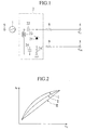
- FIG. 1 is a circuit diagram showing an FM signal oscillator circuit according to a related art.
- This circuit includes a voltage-controlled oscillator having a resonator that employs a variable capacitance diode to provide an FM signal. More precisely, the FM signal oscillator circuit has a driver 1, the resonator 2, and resistors 8 and 9 to supply a control voltage Vc and a modulating signal Vm to the resonator 2.
- the resonator 2 is an LC resonator including the variable capacitance diode 21, a capacitor 22, a coil 23, a capacitor 24, and a resistor 25.
- the capacitor 24 and resistor 25 form a parallel circuit.
- the driver 1 and resonator 2 form the voltage-controlled oscillator.
- the control voltage Vc is supplied to a frequency control input terminal 4 from which to the resistor 8 and then to a cathode of the diode 21.
- the control voltage Vc determines a capacitance of the diode 21, and thus, a resonance frequency of the resonator 2 or an oscillation frequency fo of the voltage-controlled oscillator composed of the driver 1 and resonator 2.
- An output terminal 6 provides an oscillating output signal.
- the modulating signal Vm is supplied to an input terminal 5 from which to the resistor 9 and then to an anode of the diode 21.
- the capacitance of the diode 21 slightly changes to change the resonance frequency of the resonator 2 around fo, thereby provide an FM signal from the output terminal 6.
- variable capacitance diode 21 of the resonator 2 must have a hyper abrupt junction, so that the voltage-controlled oscillator may maintain a constant modulation level even if the control voltage Vc is changed.
- the oscillation frequency fo must be changed by changing the control voltage Vc without fluctuating a modulation level.
- Figure 2 is a graph showing the control voltage (Vc)-oscillation frequency (fo) characteristics of variable capacitance diodes with graded junction (I), abrupt junction (II), and hyper abrupt junction (III).
- the hyper-abrupt-junction diode (III) shows linear Vc-fo characteristics to maintain a constant modulation level even if the control voltage Vc is changed to vary the oscillation frequency fo.
- the graded-junction diode (I) and abrupt-junction diode (II) show nonlinear Vc-fo characteristics to alter a modulation level when the control voltage Vc is changed to change the oscillation frequency fo.
- a problem of the FM signal oscillator circuit employing the hyper-abrupt-junction diode is that it is unable to produce through standard IC (integrated circuit) manufacturing processes because the standard processes are only capable of forming abrupt- or graded-junction diodes on ICs.
- IC integrated circuit
- the present invention is to provide an FM signal oscillator circuit and a modulation level control method, capable of employing abrupt- or graded-junction variable capacitance diodes for a resonator without changing a modulation level, so that the circuit may be produced as an IC through standard IC manufacturing processes.
- An FM signal oscillator circuit includes a resonator having a variable capacitance diode whose capacitance is set according to a control voltage, the variable capacitance diode changing a resonance frequency of the resonator, a driver configured to drive the resonator and providing an FM signal, a corrector configured to correct the level of a modulating signal according to resonance-frequency-changing characteristics of the resonator and applying a signal corresponding to the corrected modulating signal and a signal corresponding to the control voltage to the variable capacitance diode.
- the FM signal oscillator circuit according to this invention enables to employ graded- or abrupt-junction variable capacitance diodes to fabricate a resonator of the FM signal oscillator circuit that is capable of maintaining a constant modulation level when an oscillation frequency is changed. Due to the graded- or abrupt-junction diodes, this oscillator circuit is manufacturable through standard IC manufacturing processes at low cost.
- Figure 3 is a flowchart showing a modulation level control method according to an embodiment of the present invention.
- the method sets a center frequency according to a control signal, receives a modulating signal, modulates the center frequency according to the modulating signal in an oscillator having a variable capacitance element, and provides an FM (frequency-modulated) oscillating signal.
- Step S101 receives the control signal and amplifies the same through an amplifier.
- Step S102 amplifies the modulating signal according to a gain determined by the amplified control signal.
- this embodiment according to the invention substantially maintains the frequency modulation gain of the oscillator.
- Step S103 adds the amplified modulating signal to the control signal.
- Step S104 applies the sum to the variable capacitance element to control the resonance frequency of the oscillator.
- FIG. 4 is a circuit diagram showing an FM signal oscillator circuit according to the first embodiment of the present invention.
- the FM signal oscillator circuit includes a driver 1, a resonator 2, a modulating signal corrector 3, an input terminal 4 for receiving a control voltage Vc to set a center oscillation frequency fo, an input terminal 5 for receiving a modulating signal Vm, and an output terminal 6 for providing an FM (frequency-modulated) signal having the center frequency of fo.
- the resonator 2 includes a variable capacitance diode 21, a capacitor 22, and a coil 23.
- the corrector 3 includes an operational amplifier 31, a variable gain amplifier 32, an adder 33, and a resistor 34.
- the diode 21 has, for example, a graded junction so that the diode 21 may be manufactured on a semiconductor IC through standard IC manufacturing processes.
- the control voltage Vc is received through the input terminal 4 and is amplified by the operational amplifier 31.
- the amplified control voltage is supplied to a control terminal of the variable gain amplifier 32, to set an amplification gain of the amplifier 32.
- the modulating signal Vm is received through the input terminal 5 and is amplified by the amplifier 32 according to the set gain, to provide an amplified modulating signal Vmc to the adder 33.
- the adder 33 adds or superimposes the amplified modulating signal Vmc to the control voltage Vc.
- the superimposed signal is passed through the resistor 34 and is applied to a cathode of the variable capacitance diode 21.
- the capacitance of the diode 21 is minutely changed by the amplified modulating signal Vmc around a capacitance value determined by the control voltage Vc.
- the driver 1 and resonator 2 provide, through the output terminal 6, an FM signal that varies according to the signal Vmc around the frequency fo determined by the control voltage Vc.
- a modulation level of the FM signal is determined by the signal Vmc, i.e., the gain of the variable gain amplifier 32 that is dependent on the control voltage Vc.
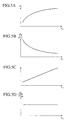
- variable capacitance diode 21 has a graded junction and if no measures are taken to deal with the graded junction, the control voltage Vc to the input terminal 4 and the oscillating frequency fo of a voltage-controlled oscillator consisting of the driver 1 and resonator 2 show a relationship of Fig. 5A.
- the ratio "dfo/dVc" of a variation in fo to a change in Vc is as shown in Fig. 5B.
- the modulating signal Vm to the input terminal 5 is passed through the variable gain amplifier 32 having a gain characteristic curve of Fig. 5C, to provide the amplified modulating signal Vmc, which is added to the control voltage Vc in the adder 33 and is applied to the variable capacitance diode 21.
- a change in the control voltage Vc causes no change in a modulation level "dfo/dVm" with respect to the modulation signal Vm.
- a constant modulation level is maintained irrespective of a change in the control voltage Vc or oscillation frequency fo, by setting the gain of the variable gain amplifier 32 in response to the control voltage Vc.
- the Vc-fo characteristics of Fig. 5A may be influenced by a graded-junction factor of the diode 21, the characteristics of the driver 1, and other factors. To cope with this, the gain control characteristics of the variable gain amplifier 32 may be adjusted to substantially maintain a constant modulation level with respect to the modulating signal Vm.
- FIG. 6 is a circuit diagram showing the details of the operational amplifier 31 of Fig. 4.
- Transistors T1 and T2 form a differential amplification stage that amplifies the control voltage Vc provided through the input terminal 4 (61).
- An input terminal 62 is grounded.
- Transistors T3 and T4 form a current mirror circuit, and therefore, a current passing through the transistors T1 and T3 is equal to a current passing through the transistor T4.
- Transistors T5 and T6 form a current mirror circuit, and therefore, a current passing through the transistors T2 and T5 is equal to a current passing through the transistors T6 and T7.
- the transistor T7 and a transistor T8 form a current mirror circuit, and therefore, a current passing through the transistors T6 and T7 is equal to a current passing through the transistor T8.
- an output terminal 63 provides a voltage corresponding to a difference between the currents passing through the transistors T4 and T8.
- the operational amplifier 31 may be applicable to a comparator 39 to be explained later with reference to the third embodiment of Fig. 9.
- the input terminal 61 receives the control voltage and the input terminal 62 receives a voltage from resistors 37 and 38, so that the comparator 39 may provide a differential voltage.
- FIG. 7 is a circuit diagram showing the details of the variable gain amplifier 32.
- Transistors T9 and T10 form an amplification stage.
- Transistors T13 and T14 form a current source and a current mirror circuit.
- the modulating signal Vm is received through the input terminal 5 and is amplified by the transistors T9 and T10.
- the amplified current is supplied to the transistor T11.
- the transistor T11 and a transistor T12 form a current mirror circuit, and therefore, the amplified current is passed through the transistor T12, to provide the amplified modulating signal Vmc from an emitter of the transistor 12.
- a control terminal 63 receives the amplified control voltage from the operational amplifier 31, to change the current passing through the transistor T14. This changes the current passing through the transistor T13. Namely, the current of the current source connected to the amplification stage consisting of the transistors T9 and T10 changes to change an amplification gain of the amplification stage. This realizes variable gain amplification.
- variable capacitance diode 21 of the resonator 2 may have a graded junction to cause a nonlinear relationship between the control voltage Vc and the oscillation frequency fo. Even so, the embodiment uses the control voltage Vc to change the amplification gain of the variable gain amplifier 32 working on the modulating signal Vm, to maintain a constant modulation level irrespective of a change in the control voltage Vc, i.e., a change in the oscillation frequency fo.
- the embodiment is capable of maintaining a constant modulation level with respect to every frequency to which the oscillation frequency fo is changed by changing the control voltage Vc.
- the variable capacitance diode 21 of the resonator 2 is producible through standard IC manufacturing processes without additional processes, to provide an integrated FM signal oscillator circuit.
- the FM signal oscillator circuit thus produced is of low cost and is capable of maintaining a constant modulation level even if a center oscillation frequency fo is changed by changing a control voltage Vc.
- FIG 8 is a circuit diagram showing an FM signal oscillator circuit according to the second embodiment of the present invention.
- This circuit includes a driver 1, a resonator 2, and a modulating signal corrector 3 like the first embodiment of Fig. 4.
- the second embodiment differs from the first embodiment in that an amplified modulating signal Vmc from a variable gain amplifier 32 is passed through a resistor 35 and is applied to an anode of a graded-junction variable capacitance diode 21 contained in the resonator 2, and in that a control voltage Vc is passed through a resistor 36 and is applied to a cathode of the diode 21.
- the second embodiment eliminates the adder 33 of the first embodiment.
- the second embodiment applies the control voltage Vc and amplified modulating signal Vmc to the cathode and anode of the variable capacitance diode 21, to realize the same effect as that of the first embodiment without an adder.
- the second embodiment arranges a parallel circuit consisting of a capacitor 24 and a resistor 25, to apply the amplified modulating signal Vmc to the diode 21.
- FIG. 9 is a circuit diagram showing an FM signal oscillator circuit according to the third embodiment of the present invention.
- This circuit includes a driver 1, a resonator 2, a modulating signal corrector 3, and a current supply circuit 7.
- the driver 1 and resonator 2 form a differential voltage controlled oscillator.
- the driver 1 includes oscillating transistors 11 and 12 and a resistor 13.
- the resonator 2 includes two variable capacitance diodes 21 and a coil 23.
- the diodes 21 have graded junctions and commonly-connected cathodes.
- the corrector 3 includes a comparator 39, a variable gain amplifier 32, and resistors 37 and 38.
- the resistors 37 and 38 pick up a midpoint voltage of the diodes 21.
- a control voltage Vc is received through a frequency control input terminal 4 and is applied to a positive input terminal of the comparator 39.
- the control voltage Vc is also applied to the cathodes of the diodes 21.
- a negative input terminal of the comparator 39 receives an anode voltage of the diodes 21 through the resistors 37 and 38.
- the comparator 39 compares the control voltage Vc with the anode voltage and provides a differential voltage (corresponding to a terminal voltage of the diodes 21) to a control terminal of the variable gain amplifier 32, to set an amplification gain of the amplifier 32.
- a modulating signal Vm is received through an input terminal 5 and is amplified by the amplifier 32 according to the set gain, to provide an amplified modulating signal Vmc.
- the signal Vmc is supplied to a common emitter of the transistors 11 and 12 of the driver 1.
- the diodes 21 receive the sum of Vc and Vmc, so that the capacitance of the diodes 21 is set according to the control voltage Vc and is minutely changed according to the amplified modulating signal Vmc.
- the oscillating transistors 11 and 12 of the driver 1 produce an FM oscillating signal having a center frequency of fo, and the oscillating output (differential output) is provided outside from output terminals 41 and 42 connected to collectors of the transistors 11 and 12.
- the current supply circuit 7 has current sources 71 and 72 that receive a reference voltage and provide operation currents to the driver 1 through the resonator 2.
- a modulation level of the FM signal is determined by the level of the amplified modulating signal Vmc and is controlled by the gain of the amplifier 32 that is dependent on the control voltage Vc.
- the third embodiment applies the sum of Vc and Vmc to the diode 21.
- the third embodiment is similar to the first embodiment of Fig. 4.
- the third embodiment forms the resonator 2 with the variable capacitance diodes 21 of graded junction manufacturable through standard IC manufacturing processes.
- the third embodiment maintains a constant modulation level of the modulating signal Vmc, like the first embodiment.
- the present invention may also employ abrupt-junction diodes as the diodes 21 with the same modulating signal corrector 3, to realize the effect of the present invention.
- the present invention employs graded- or abrupt-junction variable capacitance diodes to fabricate a resonator of an FM signal oscillator circuit that is capable of maintaining a constant modulation level when an oscillation frequency is changed. Due to the graded- or abrupt-junction diodes, this oscillator circuit is manufacturable through standard IC manufacturing processes at low cost.
Landscapes
- Engineering & Computer Science (AREA)
- Computer Networks & Wireless Communication (AREA)
- Signal Processing (AREA)
- Inductance-Capacitance Distribution Constants And Capacitance-Resistance Oscillators (AREA)
- Digital Transmission Methods That Use Modulated Carrier Waves (AREA)
Abstract
Description
Claims (13)
- An FM signal oscillator circuit comprising:a resonator having a variable capacitance diode whose capacitance is set according to a control voltage, the variable capacitance diode changing a resonance frequency of the resonator;a driver configured to drive the resonator and providing an FM signal; anda corrector configured to correct the level of a modulating signal according to resonance-frequency-changing characteristics of the resonator and applying a signal corresponding to the corrected modulating signal and a signal corresponding to the control voltage to the variable capacitance diode.
- The FM signal oscillator circuit as claimed in claim 1, wherein:the corrector changes the level of the modulating signal according to a terminal voltage of the variable capacitance diode.
- The FM signal oscillator circuit as claimed in claim 1, wherein:the corrector changes the level of the modulating signal according to the control voltage.
- The FM signal oscillator circuit as claimed in claim 3, wherein:the corrector has a variable gain amplifier that changes an amplification gain according to the control voltage and sets the level of the modulating signal.
- The FM signal oscillator circuit as claimed in claim 1, wherein the corrector comprises:an operational amplifier configured to amplify the control voltage;a variable gain amplifier configured to amplify the modulating signal according to the amplified control voltage; andan adder configured to add the control voltage and the amplified modulating signal to each other, and the adder further configured to apply the sum to the variable capacitance diode.
- The FM signal oscillator circuit as claimed in claim 1, wherein the corrector comprises:an operational amplifier configured to amplify the control voltage; anda variable gain amplifier configured to amplify the modulating signal according to the amplified control voltage,the corrector applying the control voltage and the amplified modulating signal to opposite ends of the variable capacitance diode, respectively.
- The FM signal oscillator circuit as claimed in claim 1, wherein:the resonator includes two variable capacitance diodes to form, together with the driver, a differential voltage controlled oscillator; andthe corrector includes:a comparator configured to compare a signal corresponding to the control voltage applied to a common cathode of the variable capacitance diodes with a signal corresponding to an anode voltage of the variable capacitance diodes and providing a differential voltage based on the compared voltages, anda variable gain amplifier whose amplification gain is changed according to the differential voltage, configured to set the level of the modulating signal.
- The FM signal oscillator circuit as claimed in claim 1, wherein the variable capacitance diode has one of a graded junction and an abrupt junction.
- The FM signal oscillator circuit as claimed in claim 1, wherein the FM signal oscillator circuit is a semiconductor integrated circuit.
- A modulation level controlling method for an oscillator having a variable capacitance element to provide an FM signal having a center frequency determined by a control signal and modulated by a modulating signal, the method comprising:amplifying the control signal;amplifying the modulating signal according to a gain determined by the amplified control signal;adding the amplified modulating signal to the control signal, to form a sum signal; andapplying the sum signal to the variable capacitance element to control a resonance frequency in the oscillator.
- The method as claimed in claim 10, wherein the modulating signal is amplified in such a way as to maintain a constant modulation gain for an oscillation frequency of the oscillator.
- A modulation level controlling method for an oscillator having a variable capacitance element to provide an FM signal having a center frequency determined by a control signal and modulated by a modulating signal, the method comprising:amplifying the control signal;amplifying the modulating signal according to a gain determined by the amplified control signal; andsuperimposing the amplified modulating signal on the control signal in such a way as to maintain a constant modulation gain for an oscillation frequency of the oscillator with respect to the modulating signal, and applying the superimposed signal to the variable capacitance element to control a resonance frequency in the oscillator.
- A modulation level controlling method for an oscillator having a variable capacitance element to provide an FM signal having a center frequency determined by a control signal and modulated by a modulating signal, the method comprising:extracting a terminal voltage of the variable capacitance element based on the control signal serving as a comparison reference;amplifying the modulating signal by a gain determined from the extracted terminal voltage; andsupplying the amplified modulating signal to the oscillator to control a resonance frequency in the oscillator in such a way as to maintain a constant modulation gain for an oscillation frequency of the oscillator with respect to the modulating signal.
Applications Claiming Priority (2)
| Application Number | Priority Date | Filing Date | Title |
|---|---|---|---|
| JP2000199437A JP2002016442A (en) | 2000-06-30 | 2000-06-30 | FM signal oscillation circuit and modulation level correction method |
| JP2000199437 | 2000-06-30 |
Publications (2)
| Publication Number | Publication Date |
|---|---|
| EP1175002A2 true EP1175002A2 (en) | 2002-01-23 |
| EP1175002A3 EP1175002A3 (en) | 2003-04-23 |
Family
ID=18697456
Family Applications (1)
| Application Number | Title | Priority Date | Filing Date |
|---|---|---|---|
| EP01114753A Withdrawn EP1175002A3 (en) | 2000-06-30 | 2001-06-22 | FM signal oscillator circuit and modulation level control method |
Country Status (6)
| Country | Link |
|---|---|
| US (1) | US6545557B2 (en) |
| EP (1) | EP1175002A3 (en) |
| JP (1) | JP2002016442A (en) |
| KR (1) | KR100412002B1 (en) |
| CN (1) | CN1168200C (en) |
| TW (1) | TW504894B (en) |
Families Citing this family (6)
| Publication number | Priority date | Publication date | Assignee | Title |
|---|---|---|---|---|
| US7885337B2 (en) * | 2004-08-23 | 2011-02-08 | Qualcomm Incorporated | Efficient video slicing |
| US20060062312A1 (en) * | 2004-09-22 | 2006-03-23 | Yen-Chi Lee | Video demultiplexer and decoder with efficient data recovery |
| US8379733B2 (en) * | 2006-09-26 | 2013-02-19 | Qualcomm Incorporated | Efficient video packetization methods for packet-switched video telephony applications |
| JP4940880B2 (en) * | 2006-10-13 | 2012-05-30 | 日本電気株式会社 | Voltage controlled oscillator |
| US9357233B2 (en) * | 2008-02-26 | 2016-05-31 | Qualcomm Incorporated | Video decoder error handling |
| CN102157792B (en) * | 2011-02-14 | 2014-03-26 | 中国科学院光电技术研究所 | Electric control radiation pattern reconfigurable antenna |
Family Cites Families (8)
| Publication number | Priority date | Publication date | Assignee | Title |
|---|---|---|---|---|
| JPH0354903A (en) * | 1989-03-31 | 1991-03-08 | Kyocera Corp | Oscillation circuit |
| JPH10150321A (en) * | 1996-11-18 | 1998-06-02 | Murata Mfg Co Ltd | Voltage controlled oscillator |
| KR100224310B1 (en) * | 1996-12-05 | 1999-10-15 | 정선종 | Cmos voltage controll oscillator |
| JPH10270937A (en) * | 1997-03-27 | 1998-10-09 | Murata Mfg Co Ltd | Voltage controlled oscillator |
| JPH1197928A (en) | 1997-09-19 | 1999-04-09 | Nippon Telegr & Teleph Corp <Ntt> | Voltage controlled oscillator |
| US5952895A (en) * | 1998-02-23 | 1999-09-14 | Tropian, Inc. | Direct digital synthesis of precise, stable angle modulated RF signal |
| JP2000307344A (en) * | 1999-04-16 | 2000-11-02 | Fujitsu Ltd | Voltage controlled oscillator and semiconductor integrated circuit device |
| US6362698B1 (en) * | 2000-09-29 | 2002-03-26 | Intel Corporation | Low impedance clamping buffer for an LC tank VCO |
-
2000
- 2000-06-30 JP JP2000199437A patent/JP2002016442A/en not_active Abandoned
-
2001
- 2001-05-31 TW TW090113156A patent/TW504894B/en not_active IP Right Cessation
- 2001-06-15 US US09/880,918 patent/US6545557B2/en not_active Expired - Fee Related
- 2001-06-22 EP EP01114753A patent/EP1175002A3/en not_active Withdrawn
- 2001-06-29 CN CNB011218495A patent/CN1168200C/en not_active Expired - Fee Related
- 2001-06-29 KR KR10-2001-0037994A patent/KR100412002B1/en not_active Expired - Fee Related
Also Published As
| Publication number | Publication date |
|---|---|
| CN1339872A (en) | 2002-03-13 |
| JP2002016442A (en) | 2002-01-18 |
| US6545557B2 (en) | 2003-04-08 |
| US20020027479A1 (en) | 2002-03-07 |
| KR20020002293A (en) | 2002-01-09 |
| EP1175002A3 (en) | 2003-04-23 |
| TW504894B (en) | 2002-10-01 |
| CN1168200C (en) | 2004-09-22 |
| KR100412002B1 (en) | 2003-12-24 |
Similar Documents
| Publication | Publication Date | Title |
|---|---|---|
| JP4369422B2 (en) | Trimming of two-point phase modulator | |
| US6137375A (en) | Loss control loop circuit for controlling the output voltage of a voltage-controlled oscillator | |
| US20050179484A1 (en) | Bias voltage supply circuit and radio-frequency amplification circuit | |
| US6545557B2 (en) | FM signal oscillator circuit and modulation level control method | |
| KR100871516B1 (en) | Output voltage modulation method of transmitter circuit and transmitter circuit | |
| US6411170B2 (en) | Oscillation circuit | |
| JP2003046335A (en) | Temperature compensated crystal oscillator | |
| CA2253586A1 (en) | Bridge-stabilized oscillator circuit and method | |
| EP0357996B1 (en) | Frequency modulator utilizing frequency synthesizer | |
| JP3154207B2 (en) | Detector and transmitter | |
| US5357222A (en) | Voltage controlled component including a capacitive diode biased to operate in the linear region | |
| KR0146364B1 (en) | Frequency modulator | |
| JPH04253405A (en) | Oscillator output signal amplitude adjustment method and oscillator amplifier circuit device | |
| JP2000516430A (en) | Compensation for oscillator frequency shift | |
| US6353370B1 (en) | Method and apparatus for modulation of a voltage controlled oscillator | |
| US4383136A (en) | Muting circuit for AM stereophonic receiver | |
| US4630008A (en) | Direct FM crystal-controlled oscillator | |
| JP3400911B2 (en) | Gate bias voltage generation circuit | |
| US4616186A (en) | FM quadrature demodulator with distortion compensation | |
| JPH0618289B2 (en) | Oscillator circuit | |
| JPH07254818A (en) | Voltage controlled oscillator | |
| JP2002084135A (en) | Voltage controlled oscillator | |
| JPH0317454Y2 (en) | ||
| JPH03238905A (en) | oscillation circuit | |
| JP2005260797A (en) | Voltage controlled oscillator |
Legal Events
| Date | Code | Title | Description |
|---|---|---|---|
| PUAI | Public reference made under article 153(3) epc to a published international application that has entered the european phase |
Free format text: ORIGINAL CODE: 0009012 |
|
| 17P | Request for examination filed |
Effective date: 20010622 |
|
| AK | Designated contracting states |
Kind code of ref document: A2 Designated state(s): AT BE CH CY DE DK ES FI FR GB GR IE IT LI LU MC NL PT SE TR |
|
| AX | Request for extension of the european patent |
Free format text: AL;LT;LV;MK;RO;SI |
|
| PUAL | Search report despatched |
Free format text: ORIGINAL CODE: 0009013 |
|
| AK | Designated contracting states |
Designated state(s): AT BE CH CY DE DK ES FI FR GB GR IE IT LI LU MC NL PT SE TR |
|
| AX | Request for extension of the european patent |
Extension state: AL LT LV MK RO SI |
|
| RIC1 | Information provided on ipc code assigned before grant |
Ipc: 7H 03C 3/22 B Ipc: 7H 03C 3/04 A |
|
| AKX | Designation fees paid |
Designated state(s): DE FR GB |
|
| 17Q | First examination report despatched |
Effective date: 20080603 |
|
| STAA | Information on the status of an ep patent application or granted ep patent |
Free format text: STATUS: THE APPLICATION IS DEEMED TO BE WITHDRAWN |
|
| 18D | Application deemed to be withdrawn |
Effective date: 20081014 |