EP1174853A2 - Driving method for display device, driving circuit, display device, and electronic apparatus - Google Patents
Driving method for display device, driving circuit, display device, and electronic apparatus Download PDFInfo
- Publication number
- EP1174853A2 EP1174853A2 EP01306150A EP01306150A EP1174853A2 EP 1174853 A2 EP1174853 A2 EP 1174853A2 EP 01306150 A EP01306150 A EP 01306150A EP 01306150 A EP01306150 A EP 01306150A EP 1174853 A2 EP1174853 A2 EP 1174853A2
- Authority
- EP
- European Patent Office
- Prior art keywords
- time period
- voltage
- scanning
- line
- scanning line
- Prior art date
- Legal status (The legal status is an assumption and is not a legal conclusion. Google has not performed a legal analysis and makes no representation as to the accuracy of the status listed.)
- Withdrawn
Links
Images










Classifications
-
- G—PHYSICS
- G09—EDUCATION; CRYPTOGRAPHY; DISPLAY; ADVERTISING; SEALS
- G09G—ARRANGEMENTS OR CIRCUITS FOR CONTROL OF INDICATING DEVICES USING STATIC MEANS TO PRESENT VARIABLE INFORMATION
- G09G3/00—Control arrangements or circuits, of interest only in connection with visual indicators other than cathode-ray tubes
- G09G3/20—Control arrangements or circuits, of interest only in connection with visual indicators other than cathode-ray tubes for presentation of an assembly of a number of characters, e.g. a page, by composing the assembly by combination of individual elements arranged in a matrix no fixed position being assigned to or needed to be assigned to the individual characters or partial characters
- G09G3/34—Control arrangements or circuits, of interest only in connection with visual indicators other than cathode-ray tubes for presentation of an assembly of a number of characters, e.g. a page, by composing the assembly by combination of individual elements arranged in a matrix no fixed position being assigned to or needed to be assigned to the individual characters or partial characters by control of light from an independent source
- G09G3/36—Control arrangements or circuits, of interest only in connection with visual indicators other than cathode-ray tubes for presentation of an assembly of a number of characters, e.g. a page, by composing the assembly by combination of individual elements arranged in a matrix no fixed position being assigned to or needed to be assigned to the individual characters or partial characters by control of light from an independent source using liquid crystals
-
- G—PHYSICS
- G09—EDUCATION; CRYPTOGRAPHY; DISPLAY; ADVERTISING; SEALS
- G09G—ARRANGEMENTS OR CIRCUITS FOR CONTROL OF INDICATING DEVICES USING STATIC MEANS TO PRESENT VARIABLE INFORMATION
- G09G3/00—Control arrangements or circuits, of interest only in connection with visual indicators other than cathode-ray tubes
- G09G3/20—Control arrangements or circuits, of interest only in connection with visual indicators other than cathode-ray tubes for presentation of an assembly of a number of characters, e.g. a page, by composing the assembly by combination of individual elements arranged in a matrix no fixed position being assigned to or needed to be assigned to the individual characters or partial characters
- G09G3/34—Control arrangements or circuits, of interest only in connection with visual indicators other than cathode-ray tubes for presentation of an assembly of a number of characters, e.g. a page, by composing the assembly by combination of individual elements arranged in a matrix no fixed position being assigned to or needed to be assigned to the individual characters or partial characters by control of light from an independent source
- G09G3/36—Control arrangements or circuits, of interest only in connection with visual indicators other than cathode-ray tubes for presentation of an assembly of a number of characters, e.g. a page, by composing the assembly by combination of individual elements arranged in a matrix no fixed position being assigned to or needed to be assigned to the individual characters or partial characters by control of light from an independent source using liquid crystals
- G09G3/3611—Control of matrices with row and column drivers
- G09G3/3614—Control of polarity reversal in general
-
- G—PHYSICS
- G09—EDUCATION; CRYPTOGRAPHY; DISPLAY; ADVERTISING; SEALS
- G09G—ARRANGEMENTS OR CIRCUITS FOR CONTROL OF INDICATING DEVICES USING STATIC MEANS TO PRESENT VARIABLE INFORMATION
- G09G3/00—Control arrangements or circuits, of interest only in connection with visual indicators other than cathode-ray tubes
- G09G3/20—Control arrangements or circuits, of interest only in connection with visual indicators other than cathode-ray tubes for presentation of an assembly of a number of characters, e.g. a page, by composing the assembly by combination of individual elements arranged in a matrix no fixed position being assigned to or needed to be assigned to the individual characters or partial characters
- G09G3/34—Control arrangements or circuits, of interest only in connection with visual indicators other than cathode-ray tubes for presentation of an assembly of a number of characters, e.g. a page, by composing the assembly by combination of individual elements arranged in a matrix no fixed position being assigned to or needed to be assigned to the individual characters or partial characters by control of light from an independent source
- G09G3/36—Control arrangements or circuits, of interest only in connection with visual indicators other than cathode-ray tubes for presentation of an assembly of a number of characters, e.g. a page, by composing the assembly by combination of individual elements arranged in a matrix no fixed position being assigned to or needed to be assigned to the individual characters or partial characters by control of light from an independent source using liquid crystals
- G09G3/3611—Control of matrices with row and column drivers
- G09G3/367—Control of matrices with row and column drivers with a nonlinear element in series with the liquid crystal cell, e.g. a diode, or M.I.M. element
-
- G—PHYSICS
- G09—EDUCATION; CRYPTOGRAPHY; DISPLAY; ADVERTISING; SEALS
- G09G—ARRANGEMENTS OR CIRCUITS FOR CONTROL OF INDICATING DEVICES USING STATIC MEANS TO PRESENT VARIABLE INFORMATION
- G09G2310/00—Command of the display device
- G09G2310/06—Details of flat display driving waveforms
-
- G—PHYSICS
- G09—EDUCATION; CRYPTOGRAPHY; DISPLAY; ADVERTISING; SEALS
- G09G—ARRANGEMENTS OR CIRCUITS FOR CONTROL OF INDICATING DEVICES USING STATIC MEANS TO PRESENT VARIABLE INFORMATION
- G09G2320/00—Control of display operating conditions
- G09G2320/02—Improving the quality of display appearance
- G09G2320/0209—Crosstalk reduction, i.e. to reduce direct or indirect influences of signals directed to a certain pixel of the displayed image on other pixels of said image, inclusive of influences affecting pixels in different frames or fields or sub-images which constitute a same image, e.g. left and right images of a stereoscopic display
-
- G—PHYSICS
- G09—EDUCATION; CRYPTOGRAPHY; DISPLAY; ADVERTISING; SEALS
- G09G—ARRANGEMENTS OR CIRCUITS FOR CONTROL OF INDICATING DEVICES USING STATIC MEANS TO PRESENT VARIABLE INFORMATION
- G09G2330/00—Aspects of power supply; Aspects of display protection and defect management
- G09G2330/02—Details of power systems and of start or stop of display operation
- G09G2330/021—Power management, e.g. power saving
-
- G—PHYSICS
- G09—EDUCATION; CRYPTOGRAPHY; DISPLAY; ADVERTISING; SEALS
- G09G—ARRANGEMENTS OR CIRCUITS FOR CONTROL OF INDICATING DEVICES USING STATIC MEANS TO PRESENT VARIABLE INFORMATION
- G09G2330/00—Aspects of power supply; Aspects of display protection and defect management
- G09G2330/02—Details of power systems and of start or stop of display operation
- G09G2330/021—Power management, e.g. power saving
- G09G2330/023—Power management, e.g. power saving using energy recovery or conservation
-
- G—PHYSICS
- G09—EDUCATION; CRYPTOGRAPHY; DISPLAY; ADVERTISING; SEALS
- G09G—ARRANGEMENTS OR CIRCUITS FOR CONTROL OF INDICATING DEVICES USING STATIC MEANS TO PRESENT VARIABLE INFORMATION
- G09G3/00—Control arrangements or circuits, of interest only in connection with visual indicators other than cathode-ray tubes
- G09G3/20—Control arrangements or circuits, of interest only in connection with visual indicators other than cathode-ray tubes for presentation of an assembly of a number of characters, e.g. a page, by composing the assembly by combination of individual elements arranged in a matrix no fixed position being assigned to or needed to be assigned to the individual characters or partial characters
- G09G3/2007—Display of intermediate tones
- G09G3/2014—Display of intermediate tones by modulation of the duration of a single pulse during which the logic level remains constant
Definitions
- the present invention relates to a method for driving a display device, which reduces the power consumption by putting only a pixel belonging to a specific data line into a display state, while putting pixels belonging to other data lines into a non-display state, to a driving circuit for a display device, a display device, and an electronic apparatus.
- the number of display dots has increased year after year so that more information can be displayed.
- portable electronic apparatuses are battery driven in principle, they are strongly required to reduce the power consumption. For this reason, the display device used in the portable electronic apparatuses is required to have two apparently contradictory features of high resolution and low power consumption.
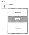
- the following driving method called a partial display driving (also referred to as a partial driving) has been proposed. That is, the partial display driving is such that, when a full-screen display operation is not particularly required, such as during standby, scanning signals are supplied only to a part of scanning lines, whereby only a region of pixels belonging to the part of the scanning lines is put into a display state, while other regions of pixels are put into a non-display state, as shown in Fig. 26 to suppress the power consumption.
- a display region (non-display region) is necessarily long sideways in accordance with a direction of formation of scanning lines, so that a display mode in the partial display is restricted in this sense.
- a display operation is performed in which a display region is long lengthways, with a configuration in which a non-lighting voltage is simply supplied to data lines included in a non-display region, a switching frequency of the voltage applied to the data lines is not decreased, so that the power consumption is ineffectively reduced.
- the present invention is made in view of the above circumstances, and an object is to provide a method for driving a display device in which a display region is long lengthways, and which can suppress the power consumption, a driving circuit therefor, a display device and an electronic apparatus.
- a method for driving a display device driving a pixel provided corresponding to each of intersections between a plurality of scanning lines and a plurality of data lines wherein one scanning line in the plurality of scanning lines is selected every 1 horizontal scanning time period, and a selection voltage is applied to the selected scanning line in one of time periods, into which the 1 horizontal scanning time period is divided; the polarity of said selection voltage is reversed at least every two or more horizontal scanning time periods on the basis of an intermediate value of a lighting voltage and a non-lighting voltage applied to the data lines; when a pixel belonging to a specific data line in said plurality of data lines is put into a display state, and pixels belonging to other data lines are put into a non-display state, a lighting voltage is applied to the specific data line in 1 horizontal scanning time period, in which one scanning line in the plurality of scanning lines is selected and a selection voltage is applied to the selected scanning line, according to the contents to
- the selection voltage is applied to each of the scanning lines in one of time periods, into which the 1 horizontal scanning time period is divided.
- the lighting voltage and the non-lighting voltage are applied to the data line in the display state (specific data line) for substantially the same period in the 1 horizontal scanning time period, occurrence of crosstalk depending on a display pattern is prevented.
- the non-lighting voltage is applied to data lines in the non-display state (data lines other than the specific data line) for the 1 horizontal scanning time period, in which the scanning line is selected.
- the lighting voltage in the present case means, when attention is paid to a certain 1 horizontal scanning line, a voltage of a data signal having the polarity opposite to that of the selection voltage applied in one of the time periods
- the non-lighting voltage means, when attention is paid to a certain 1 horizontal scanning line, a voltage of a data signal having the same polarity as the selection voltage applied in one of the time periods. Therefore, even if the positive-side voltage is applied to the data line, when the selection voltage has the negative-side polarity, the voltage is the lighting voltage, and conversely, the voltage is the non-lighting voltage when the selection voltage has the positive-side polarity.
- a selection voltage is applied to the selected scanning line in the second half time period of one of time periods, into which 1 horizontal scanning time period is divided; when the next one scanning line is selected, a selection voltage is applied to the selected scanning line in the first half time period of one of time periods, into which 1 horizontal scanning time period is divided; and the selection voltage is alternately applied in one time period and in the other time period every 1 horizontal scanning time period.
- the selection voltage is alternately applied in one time period and in the other time period every 1 horizontal scanning time period in this way, in a case where ON-displayed or OFF-displayed pixels belonging to the specific data line continue, the switching frequency of the voltage applied to the data line is decreased, so that the power consumption can be further suppressed.
- a method is preferable in which, when the selection voltage is applied in the second half time period, a lighting voltage is applied to the specific data line from a point of time before an end point of the second half time by a time period according to the gray scale of a pixel corresponding to an intersection between the selected scanning line and the specific data line to the end point of the second half time period, and a non-lighting voltage is applied in the remaining time period of the second half time period; while, when the selection voltage is applied in the first half time period, a lighting voltage is applied to the specific data line from a starting point of the first half time period to a time period according to the gray scale of a pixel corresponding to an intersection between the selected scanning line and the specific data line, and a non-lighting voltage is applied in the remaining time period of the first half time period.
- a gray scale display is performed by a so-called rightward modulation method on a pixel corresponding to an intersection between an scanning line and the specific data line, while the gray scale display is performed by a so-called leftward modulation method on a pixel corresponding to an intersection between the next one scanning line and the specific data line.
- a driving circuit for a display device driving a pixel provided corresponding to each of intersections between a plurality of scanning lines and a plurality of data lines comprising: a scanning line driving circuit for selecting one scanning line in the plurality of scanning lines every 1 horizontal scanning time period, applying a selection voltage to the selected scanning line in one of time periods, into which the 1 horizontal scanning time period is divided, and reversing the polarity of said selection voltage at least every two or more horizontal scanning time periods on the basis of an intermediate value of a lighting voltage and a non-lighting voltage applied to the data lines; and a data line driving circuit for applying, when a pixel belonging to a specific data line in said plurality of data lines is put into a display state, and pixels belonging to other data lines are put into a non-display state, a lighting voltage to the specific data line in 1 horizontal scanning time period, in which one scanning line in the pluralit
- a configuration is preferable in which the scanning line driving circuit applies a selection voltage to the selected scanning line in the second half time period of one of time periods, into which 1 horizontal scanning time period is divided, when an scanning line is selected; applies a selection voltage to the selected scanning line in the first half time period of one of time periods, into which 1 horizontal scanning time period is divided, when the next one scanning line is selected; and applies the selection voltage alternately in one time period and in the other time period every 1 horizontal scanning time period.
- a configuration is preferable in which, when said selection voltage is applied in the second half time period by the scanning line driving circuit, the data line driving circuit applies a lighting voltage to the specific data line from a point of time before an end point of the second half time by a time period according to the gray scale of a pixel corresponding to an intersection between the selected scanning line and the specific data line to the end point of the second half time period, and applies a non-lighting voltage in the remaining time period of the second half time period; while, when said selection voltage is applied in the first half time period by the scanning line driving circuit, the data line driving circuit applies a lighting voltage to said specific data line from a starting point of the first half time period to a time period according to the gray scale of a pixel corresponding to an intersection between the selected scanning line and the specific data line, and applies a non-lighting voltage in the remaining time period of the first half time period.
- a display device having a pixel provided corresponding to each of intersections between a plurality of scanning lines and a plurality of data lines, the display device comprising: a scanning line driving circuit for selecting one scanning line in the plurality of scanning lines every 1 horizontal scanning time period, applying a selection voltage to the selected scanning line in one of time periods into which the 1 horizontal scanning time period is divided, and reversing the polarity of the selection voltage at least every two or more horizontal scanning time periods on the basis of an intermediate value of a lighting voltage and a non-lighting voltage applied to the data lines; and a data line driving circuit for applying, when a pixel belonging to a specific data line in the plurality of data lines is put into a display state, and pixels belonging to other data lines are put into a non-display state, a lighting voltage to the specific data line in 1 horizontal scanning time period, in which one scanning line in the plurality of scanning lines is selected
- the pixel includes a capacitative device consisting of a switching device and an electro-optical material, and when a selection voltage is applied to one scanning line, a switching device of the pixel belonging to the scanning line is put into a conductive state, and writing operation according to a lighting voltage applied to the corresponding data line is performed on the capacitative device corresponding to the switching device.
- a selection pixel and a non-selection pixel are electrically separated, so that excellent contrast and response are provided, and high-definition display can be performed.
- the switching device is a two-terminal switching device, and the pixel is constructed by series-connecting the two-terminal switching device and the capacitative device between a scanning line and a data line.
- a three-terminal switching device such as a transistor
- the two-terminal switching device has an advantage in that no short circuit is caused in the wiring in principle.
- the two-terminal switching device has a conductor/insulator/conductor structure connected to the scanning line or the data line.
- One of the conductors can be used as the scanning line or the data line without any change, and the insulator can be formed by anodizing the conductor, so that the manufacturing process is simplified.
- an electronic apparatus comprising the display device. Therefore, as described above, this electronic apparatus can prevent the occurrence of crosstalk and reduces the power consumption.
- Fig. 1 is a block diagram showing the electrical configuration of this display device.
- a liquid crystal panel 100 has a plurality of data lines (segment electrodes) 212 formed in such a manner as to extend in a column (Y) direction, while a plurality of scanning lines (common electrodes) 312 formed in such a manner as to extend in a line (X) direction, and a pixel 116 formed corresponding to each of intersections between the data lines 212 and the scanning lines 312.
- each pixel 116 consists of a serial connection of a liquid crystal layer 118 and a TFD (Thin Film Diode) 220, which is one example of a switching device.
- the liquid crystal layer 118 has a configuration such that liquid crystal, which is an example of electro-optical materials, is sandwiched between the scanning lines 312 serving as counter electrodes and the pixel electrodes.
- the total number of the scanning lines 312 is 200, and that the total number of the data lines 212 is 160, and this embodiment is described as a 200 ⁇ 160 matrix type display device, however, the present invention is not limited thereto.
- a Y driver 350 is generally called a scanning line driving circuit, and supplies scanning signals Y1, Y2,..., Y200 to the corresponding scanning lines 312. More specifically, the Y driver 350 according to this embodiment sequentially selects one scanning line 312 every 1 horizontal scanning time period, and a selection voltage is applied in a second half time period in the selection time period, and a non-selection voltage (holding voltage) is applied in a first half time period and a non-selected time period (holding time period) of the selection time period.
- an X driver 250 is generally called a data line driving circuit, and supplies data line signals X1, X2,..., X160 to a pixel 116, which is located on the scanning line 312 selected by the Y driver 350 via a corresponding data line 212 in accordance with display contents.
- a pixel 116 which is located on the scanning line 312 selected by the Y driver 350 via a corresponding data line 212 in accordance with display contents.
- a control circuit 400 supplies various control signals and clock signals, which will be described later, to the X driver 250 and the Y driver 350 so as to control both of the drivers.
- a driving voltage generating circuit 500 generates data signals, the voltage ⁇ V D /2, which is also used as a non-selection voltage in the scanning signals, and the voltage ⁇ V S , which is used as a selection voltage in the scanning signals, respectively.
- the polarity of the voltage supplied to the scanning lines 312 or the data lines 212 is determined on the basis of a value of an intermediate electric potential of the voltage ⁇ V D /2 applied to the data lines 212: when the electric potential to be applied is higher than the intermediate value, the electric potential is determined as being on the positive-side; when the electric potential to be applied is lower than the intermediate value, this electric potential is determined as being on the negative-side.
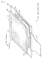
- Fig. 2 is a perspective view showing the overall configuration of the liquid crystal panel 100
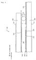
- Fig. 3 is a partially sectional view showing the configuration when the liquid crystal panel 100 is cut away along the X-direction.
- the liquid crystal panel 100 has a configuration in which a counter substrate 300 located on the side of an observer, and a device substrate 200 located on the back face thereof are bonded with maintaining a fixed gap by a seal member 110, in which a conductive particle (conductive member) 114 serving also as a spacer is mixed, and, for example, TN (Twisted Nematic) liquid crystal 160 is sealed in the gap.
- a seal member 110 is formed in the shape of a frame on one of the substrates along the inner peripheral edge of the counter substrate 300, as shown in Fig. 2 , a part thereof is opened to seal in the liquid crystal 160 therein. Therefore, after sealing in the liquid crystal, the opened part is sealed with a seal material 112.
- an alignment layer 308 is formed on an opposed face of the counter substrate 300 and a rubbing treatment is applied thereto in a predetermined direction.
- the scanning lines 312 formed on the counter substrate 300 are connected to one end of wiring 342, which is formed on the device substrate 200 and has one-to-one correspondence with each of the scanning lines 312, via the conductive particle 114 mixed in the seal member 110. That is, the scanning lines 312 formed on the counter substrate 300 are drawn out toward the device substrate 200 via the conductive particle 114 and the wiring 342.
- a polarizer 131 (omitted in Fig. 2) is bonded on the outside (observation side) of the counter substrate 300, and the absorption axis thereof is set corresponding to the direction of the rubbing treatment applied to the alignment layer 308.
- an alignment layer 208 is formed on an opposed face of the device substrate 200, and a rubbing treatment is applied thereto in a predetermined direction.
- a polarizer 121 (omitted in Fig. 2) is bonded on the outside (opposite side of the observation side) of the device substrate 200, and the absorption axis thereof is set corresponding to the direction of the rubbing treatment applied to the alignment layer 208.
- a backlight unit for uniformly illuminating light is provided on the outside of the device substrate 200, the backlight unit is not shown in the figure because it is not related directly to the present case.
- the Y driver 350 for driving the scanning lines 312, and the X driver 250 for driving the data lines 212 are mounted by a COG (Chip On Glass) technology, respectively.
- the Y driver 350 supplies scanning signals to the scanning lines 312 via the wiring 342 and the conductive particle 114, while the X driver 250 directly supplies data signals to the data lines 212.
- an FPC (Flexible Printed Circuit) board 150 is connected to the vicinity of the outside of the region, on which the X driver 250 is mounted, so as to supply various signals generated by the control circuit 400 and the drive voltage generating circuit 500 (see Fig. 1) to the Y driver 350 and the X driver 250, respectively.
- FPC Flexible Printed Circuit
- the X driver 250 and the Y driver 350 shown in Fig. 1 are, unlike shown in Fig. 2, located on the left side and the upper side of the liquid crystal panel 100, respectively, but this is only an expediential measure for describing the electrical configuration.
- a TCP Transmission Carrier Package
- a TAB Tape Automated Bonding
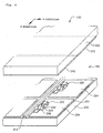
- Fig. 4 is a partially cutaway perspective view showing the structure thereof.
- the alignment layers 208 and 308 and the polarizers 121 and 131 in Fig. 3 are omitted for understanding the description.
- 200 pixel electrodes 234 arranged on the same column are commonly connected to one data line 212 via TFDs 220.
- the TFD 220 is composed of a first conductor 222 made of tantalum simple substance or tantalum alloy and branched from the data line 212, an insulator 224 obtained by anodizing the first conductor 222, and a second conductor 226, such as chromium, and has a sandwich structure of conductor/insulator/conductor.
- the TFD 220 has diode switching characteristics according to which the current-voltage characteristics become nonlinear in both the positive direction and the negative direction.
- the insulator 201 formed on the top surface of the device substrate 200 has transparency and insulating property.
- the insulator 201 is formed for reasons of preventing the first conductor 222 from being peeled off by a heat treatment after the deposition of the second conductor 226, and of preventing impurities from being diffused in the first conductor 222. Therefore, in the case where this heat treatment and the impurities present no problems, the insulator 201 can be omitted.
- the scanning lines 312 made of ITO and the like are extended on the opposed surface of the counter substrate 300 in the line direction intersecting perpendicularly to the data lines 212, and are arranged on the positions to face the pixel electrodes 234.
- color filters arranged like a stripe, a mosaic, or a triangle are provided on the counter substrate 300 according to the usage of the liquid crystal panel 100, and a black matrix is provided on a region except the color filters so as to prevent light shielding or color mixture between the pixels, a description thereof will be omitted because they are not directly related to the present case.
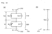
- one piece of the pixels 116 having the above-described configuration can be represented by an equivalent circuit as shown in Fig. 18(a) . That is, in general, the pixel 116 corresponding to the intersection between the scanning line 312 in the j-th (j is an integer of 1 ⁇ j ⁇ 200) line and the data line 212 in the i-th (i is an integer of 1 ⁇ i ⁇ 160) column can be represented by a series circuit of a TFD 220 shown by a parallel circuit of the resistance R T and the capacitance C T , and a liquid crystal layer 118 shown by a parallel circuit of the resistance R LC and the capacitance C LC , as shown in the figure.
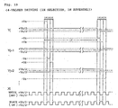
- Fig. 19 is a diagram showing waveforms of a scanning signal Yj and a data signal Xi applied to a certain pixel 116 by the four-valued driving method (1H selection, 1H reversal).
- a non-selection voltage +V D /2 is applied and held in the holding time period, and after the lapse of 1 vertical scanning time period (1 frame) 1V from the previous selection, the selection voltage -V S is applied, and the non-selection voltage -V D /2 is applied and held in the holding time period; such operations are repeated, while one of the voltages ⁇ V D /2 is applied as the data signal Xi.
- an operation of reversing the polarity of the selection voltage every 1 horizontal scanning time period 1H is also performed such that, when the selection voltage +V S is applied as the scanning signal Yj to a certain scanning line, the selection voltage -V S is applied as the scanning signal Yj+1 to the next scanning line.
- the voltage represented by the data signal Xi in this four-valued driving method (1H selection, 1H reversal) is -V D /2 in the case where the selection voltage +V S is applied and the pixel 116 is ON-displayed (for example, a black display in a normally white mode), and is +V D /2 when the pixel 116 is OFF-displayed (a white display in the normally white mode), while the voltage is +V D /2 in the case where the selection voltage -V S is applied and when the pixel 116 is ON-displayed, and is -V D /2 when the pixel 116 is OFF-displayed.
- the switching period of the voltages ⁇ V D /2 coincides with the reversal period of the scanning signal, so that the voltage represented by the data signal is fixed to one of the voltages ⁇ V D /2 in the time period, in which the scanning lines included in the region A are selected.
- the selection voltages at adjacent scanning lines have polarities opposite to each other, as described above.
- the effective value of the voltage applied in the part of the holding time period to the pixel 116 located on the odd-numbered line differs from the effective value of the voltage applied to the pixel 116 located on the even-numbered line.
- density difference is generated between the pixel 116 on the odd-numbered line and the pixel 116 on the even-numbered line, and the above-described crosstalk occurs.
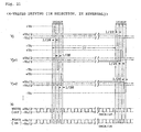
- this four-valued driving method (1/2 selection, 1H reversal) divides the 1 horizontal scanning time period 1H in the four-valued driving method (1H selection, 1H reversal) into a first half time period and a second half time period, selects the scanning line in, for example, the second half time period 1/2H, and sets the ratio between the time periods in which the voltages -V D /2 and +V D /2 are applied in the 1 horizontal scanning time period 1H to 50%.
- the total number of the scanning lines 312 is 200, so that the holding time period (non-selection time period) in the 1 vertical scanning time period is 199H, which is 199 times as long as the 1 horizontal scanning time period 1H.
- the equivalent circuit of the pixel 116 in the holding time period can be represented by the capacity C PIX consisting of a series-combined capacity of the capacity C T and the capacity C LC , as shown in Fig. 18(b) .
- the capacity C PIX is represented by (C T ⁇ C LC )/(C T +C LC ).
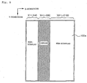
- the liquid crystal panel 100 as shown in Fig. 5, for example, a case will be considered where only the pixels located on the data lines 212 in the 41st column to 80th column counted from the left are regarded as a display region, and the pixels located on the data lines 212 in the 1st column to 40th column and in the 81st column to 160th column are regarded as non-display regions.
- a method may be simply considered for setting the data signals X41 to X80 of the data lines 212 belonging to the display region to correspond to the contents to be displayed in the display region, while setting the data signals X1 to X40 and X81 to X160 of the data lines belonging to the non-display regions to correspond to the OFF (white) display.
- the scanning line 312 on the j-th line is not selected, and the non-selection voltage represented by the scanning signal Yj applied to the scanning line is held at, for example, +V D /2
- the voltage represented by the data signal Xi to the data lines 212 corresponding to the white display is alternately switched between +V D /2 and -V D /2 every half time period (1/2H) of the 1 horizontal scanning time period 1H, so that charging and discharging are performed twice per 1 horizontal scanning time period 1H on the pixel capacity CLC (that is, the pixel capacity C PIX of the non-display region) which corresponds to the intersections between the scanning line 312 in the j-th line and the data lines in the 1st to 40th columns and 81st to 160th columns.
- the pixel capacity CLC that is, the pixel capacity C PIX of the non-display region
- the charge of C PIX ⁇ V D is supplied by the voltage switching in the holding (non-selection) time period, so that the power is consumed by the capacity load in the pixel 116.
- the display device sets the polarity reversal period of the selection signal to be two or more horizontal scanning time periods, maintains the voltage of the data signal of the data lines 212 included on the non-display region in the voltage corresponding to the OFF (white) display over the 1 horizontal scanning time period to decrease the voltage switching frequency of the data signal included in the non-display region, whereby the power consumed in the pixel of the non-display region is suppressed. Circuits for performing such a driving will now be described.
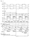
- a start pulse YD is outputted at the beginning of 1 vertical scanning time period (1 frame) as shown in Fig. 7.
- a clock signal YCLK is a scanning-line-side reference signal, and has a period of 1H that is equivalent to 1 horizontal scanning time period, as shown in Fig. 7.
- an alternate current driving signal MY is a signal for defining the polarity of a selection voltage of the scanning signal, the signal level thereof is reversed every 2 horizontal scanning time periods 2H, and the signal level is reversed every 1 vertical scanning time period in the 2 horizontal scanning time periods 2H in which the same two scanning lines are selected, as shown in Fig. 7 .
- a control signal INH is a signal for defining a time period of applying the selection voltage in the 1 horizontal scanning time period 1H, and in this embodiment, as shown in Fig. 7, the control signal has the same period as the clock signal YCLK, and is put into an H-level active in a second half time period of the 1 horizontal scanning time period 1H.
- a latch pulse LPa is a pulse outputted with the timing of changing the logical level of the alternate current driving signal MY, that is, a pulse outputted every 2 horizontal scanning time periods 2H, as shown in Fig. 9 .
- a latch pulse LP is used for latching data signals at the data-line side, and outputted at the beginning of 1 horizontal scanning time period, as shown in Fig. 9 .
- a reset signal RES is a pulse outputted at the beginning of the first half time period and at the beginning of the second half time period of 1 horizontal scanning time period at the data-line side, as shown in Fig. 9.
- an alternate current driving signal MX is a signal for defining the polarity of the data signal when it is ON-displayed, and the logical level thereof is obtained by reversing the level of the alternate current driving signal MY when the control signal INH is at an H-level (the time period in which the selection voltage is actually applied), while the logical level is obtained by maintaining the level of the alternate current driving signal MY when the control signal INH is at an L-level, as shown in Fig. 9.
- a gray scale code pulse GCP is a pulse arranged at the position of the time period on the proximal side from each of the end points of the first half time period and the second half time period, into which 1 horizontal scanning time period 1H is divided, according to the level of the intermediate gray scale, as shown in Fig. 9.
- gray scale data for designating the intensity of the pixel is represented by two bits to present a four-gray scale display, and that the gray scale data (00) designates the OFF (white) display, while the gray scale data (11) designates the ON (black) display, two gray scale code pulses GCP corresponding to gray (01) and (10) except white and black are arranged corresponding to the intermediate gray scale level in each of the first half time period and the second half time period. More specifically, the gray scale data (01) and (10) correspond to "1" and "2" of the gray scale code pulse GCP in Fig. 9. Incidentally, in Fig. 9, the gray scale code pulse GCP is actually set according to the applied voltage-intensity characteristic (V-I characteristic).
- V-I characteristic voltage-intensity characteristic
- a data PDx is a data for specifying the data line 212, which presents non-display, when the partial display is performed. For example, if the partial display is as shown in Fig. 5 , the data PDx specifies the data lines 212 in the first to 40th columns and in the 81st to 160th columns.
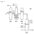
- a shift register 3502 is a 200-bit shift register which corresponds to the total number of scanning lines 312, shifts a start pulse YD supplied at the beginning of 1 frame according to clock signals YCLK having a period of 1 horizontal scanning time period, and sequentially outputs the shifted pulses as transfer signals YS1, YS2,..., YS200.
- the transfer signals YS1, YS2,..., YS200 correspond to the scanning lines 312 on the first, second, ..., 200th lines in a one-to-one correspondence relationship, and means, when one of the transfer signals is at an H-level, the scanning line 312 corresponding thereto should be selected.
- a voltage selection signal generating circuit 3504 outputs a voltage selection signal used for determining a voltage, which is to be applied to each of the scanning lines 312, from the alternate current driving signal MY and the control signal INH.
- the voltage represented by the scanning signals applied to the scanning lines 312 has the following four values: +V S (a positive-side selection voltage), +V D /2 (a positive-side non-selection voltage), -V S (a negative-side selection voltage), and -V D /2 (a negative-side non-selection voltage), as described above, and among these values, a time period, in which the selection voltage +V S or -V S is actually applied thereto, is the second half time period 1/2H of the 1 horizontal scanning time period.
- the non-selection voltage after the application of the selection voltage +V S thereto is +V D /2, and is -V D /2 after the application of the selection voltage -V S and thus, the non-selection voltage is directly and exclusively determined by the immediately preceding selection voltage.
- the voltage selection signal generating circuit 3504 generates the voltage selection signal so that the voltage level indicated by the scanning signals Y1, Y2,..., Y200 is determined as follows. That is, when one of the transfer signals YS1, YS2,... YS200 is at an H-level and selection of the scanning line 312 corresponding thereto is designated, the voltage selection signal generating circuit 3504 generates a voltage selection signal so that, first, the voltage level of the scanning signal is a selection voltage corresponding to an alternate current driving signal MY in a time period in which the control signal INH is at an H-level and second, when the signal level of the control signal INH is changed to an L-level, the signal level of the scanning signal becomes that of the non-selection voltage corresponding to the selection voltage.
- the voltage selection signal generating circuit 3504 outputs a voltage selection signal for selecting the positive-side selection voltage +V S during the time period, and thereafter, outputs a voltage selection signal for selecting the positive-side non-selection voltage +V D /2, while, in the case where the alternate current driving signal MY is at an L-level, the voltage selection signal generating circuit 3504 outputs a voltage selection signal for selecting the negative-side selection voltage -V S during the time period, and thereafter, outputs a voltage selection signal for selecting the negative-side non-selection voltage -V D /2. And, the voltage selection signal generating circuit 3504 executes the generation of such voltage selection signals corresponding to each of the 200 scanning lines 312.
- the level shifter 3506 increases the voltage amplitude of the voltage selection signal outputted by the voltage selection signal generating circuit 3504. And, the selector 3508 actually selects the voltage indicated by the voltage selection signal whose voltage amplitude is increased, and applies the voltage to each of the corresponding scanning lines 312.
- the voltage waveform of the scanning signal supplied by the Y driver 350 of the aforementioned configuration is as shown in Fig. 7. That is, the start pulse YD is sequentially shifted every 1 horizontal scanning time period 1H according to the clock signal YCLK, and such shifted pulses are outputted as the transfer signals YS1 to YS200, and the second half time period 1/2H of the 1 horizontal scanning time period 1H is selected by the control signal INH and further, the selection voltage for the scanning signal is determined according to the level of the alternate current driving signal MY in the second half time period, so that the scanning-signal voltage supplied to one scanning line is the positive-side selection voltage +V S if the alternate current driving signal MY is at, for example, an H-level in the second half time period of the 1 horizontal scanning time period in which the scanning line is selected and thereafter, the positive-side non-selection voltage +V D /2 corresponding to the selection voltage is held.
- the level of the alternate current driving signal MY is reversed to an L-level in the second half time period of the 1 horizontal scanning time period, so that the scanning-signal voltage supplied to the scanning line is the negative-side selection voltage -V S and thereafter, the negative-side non-selection voltage -V D /2 corresponding to the selection voltage is held.
- the voltage represented by the scanning signal Y1 to the scanning line 312 on the first line in an n-th frame is the positive-side selection voltage +V S in the second half time period of the horizontal scanning time period and thereafter, the positive-side non-selection voltage +V D /2 is held, and in the second half time period of the next 1 horizontal period, the level of the alternate current driving signal MY is reversed to an L-level from the previous selection, so that the voltage represented by the scanning signal Y1 to the scanning line is the negative-side selection voltage -V S and thereafter, the negative-side non-selection voltage -V D /2 is held, and such a cycle is repeated.
- the signal level of the alternate current driving signal MY is reversed every 2 horizontal scanning time periods 2H, so that the polarity of the voltage represented by the scanning signal supplied to each of the scanning lines 312 is reversed every 2 horizontal scanning time periods 2H, that is, every two scanning lines.
- the selection voltage of both of the scanning signal Y1 in the first line and the scanning signal Y2 in the second line is the positive-side selection voltage +V S and further, the selection voltage of both of the subsequent scanning signal Y3 in the third line and the scanning signal Y4 in the fourth line is the negative-side selection voltage -V S .
- FIG. 8 is a block diagram showing the configuration of this X driver 350.
- an address control circuit 2502 generates a line of address Rad used for reading gray scale data, and the address Rad is reset in response to the start pulse YD supplied at the beginning of 1 frame, and is incremented in response to a latch pulse LP supplied every 1 horizontal scanning time period.
- a display data RAM 2504 is a dual port RAM having a region corresponding to data of 200 x 160 pixels.
- a gray scale data Dn supplied from a processing circuit (not shown) is written in an address corresponding to a writing address Wad, while, on the reading side, 1 line of gray scale data (160 pieces) in the addresses designated by the address Rad are collectively read.
- a PWM decoder 2506 generates a voltage selection signal for selecting the voltages of the data signals X1, X2,..., X160 from the reset signal RES, the alternate current driving signal MX, and the gray scale code pulse GCP according to the read 1 line of gray scale data Dn.
- the voltage represented by the data signal applied to the data lines 212 is one of +V D /2 and -V D /2, and the gray scale data is 2 bits in length (4 gray scale levels), as described above.
- the PWM decoder 2506 generates voltage selection signals so that the voltage level of the data signal is established as follows with respect to each of the read 1 line of gray scale data Dn.
- the PWM decoder 2506 pays attention to one gray scale data Dn, and if the gray scale data designates an intermediate gray scale (gray) display other than the ON display and OFF display, the PWM decoder 2506 generates a voltage selection signal so that, first, the polarity thereof is reset to be opposite to the polarity represented by the logical level of the alternate current driving signal MX at the rising edge of the latch pulse LPa; second, at the falling edge of one of the gray scale code pulses GCP corresponding to the gray scale data Dn, the polarity is set to the same polarity as that represented by the logical level of the alternate current driving signal MX; and subsequently the above setting and resetting are repeated until the next latch pulse LPa is supplied.
- the PWM decoder 2506 generates a voltage selection signal using the reset signal RES and the like so that, when the gray scale data Dn is (00) corresponding to the OFF (white) display, the polarity thereof is set to be opposite to the polarity represented by the logical level of the alternate current driving signal MX, and that, when the gray scale data Dn is (11) corresponding to the ON (black) display, the polarity is set to the same polarity as that represented by the logical level of the alternate current driving signal MX.
- the PWM decoder 2506 executes the generation of such voltage selection signals corresponding to each of read 160 gray scale data Dn.
- the PWM decoder 2506 generates a voltage selection signal for the data line 212 specified by the data PDx so that the signal has the polarity represented by the logical level of the alternate current driving signal MY, regardless of the corresponding gray scale data Dn.
- the selector 2508 actually selects the voltage indicated by the voltage selection signal, which is generated by the PWM decoder 2506, and applies the selected voltage to each of the corresponding data lines 212.
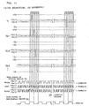
- the voltage waveforms of the data signals supplied by the X driver 250 are as shown in Fig. 9. That is, the data signal Xp (in the example shown in Fig. 5, Xp is X41 to X80) to the data lines 212 belonging to the display region corresponds to the gray scale data Dn of the pixel 116 corresponding to the intersection between the selected scanning line 312 and the corresponding data line 212 on the p-th column, and, the polarity of the data signal Xq (in the example shown in Fig.
- Xq is X1 to X40 and X81 to X160) to the data lines 212 belonging to the non-display region is the same as the polarity represented by the logical level of the alternate current driving signal MY, that is, the polarity of the selection voltage.
- Fig. 9 shows a case where the data signals Xp have the same gray scale data Dn of four pixels adjacent one to the other in the Y-direction.
- the voltage switching frequency of the data signal Xp to the data lines 212 belonging to the display region is, when the OFF (white)-displayed or ON (black)-displayed pixels continue in the column direction, 3 times per 2 horizontal scanning time periods 2H in which scanning lines having the same polarity of the selection voltage are selected, and is five times per the 2 horizontal scanning time periods 2H when the gray-displayed pixels continue in the column direction. For this reason, as simply compared with the conventional four-valued driving method (1/2 selection, 1H reversal) shown in Fig. 21 , the voltage switching frequency of the data signal included in the display region is increased.
- the voltage switching frequency of the data signal Xq to the data lines 212 belonging to the non-display region is once per the 2 horizontal scanning time periods 2H, and the voltage switching frequency is reduced by half, as compared to the case where signals corresponding to the OFF (white) display are simply supplied.
- the partial display as shown in Fig. 5 when the partial display as shown in Fig. 5 is performed, if the decrement of power consumption due to the reduction in the voltage switching frequency of the data signal Xq included in the non-display region exceeds the increment of the power consumption due to the increase in the voltage switching frequency of the data signal Xp included in the display region, the power consumption is reduced.
- the partial display as shown in Fig. 5 is performed during, such as standby, which is different from a normal operation, and only a display of minimum information is sufficient, so that a very small number of data lines 212 is required for the display region.
- the present invention is not limited thereto, and the polarity may be reversed every three or more horizontal scanning time periods.
- the polarity of the selection voltage may be reversed every 4 horizontal scanning time periods 4H.
- the voltage switching frequency of the data signal Xp to the data lines 212 belonging to the display region is, when the OFF (white)-displayed or ON (black)-displayed pixels continue in the column direction, 7 times per 4 horizontal scanning time periods 4H in which the scanning lines having the same polarity of the selection voltage are selected, and is 9 times per the four horizontal scanning time periods 4H when the gray-displayed pixels continue in the column direction.
- the voltage switching frequency of the data signal Xq to the data lines 212 belonging to the non-display region is once per the 4 horizontal scanning time periods 4H, so that the voltage switching frequency is remarkably decreased.
- the voltage switching frequency of the data signal Xp to the data lines 212 belonging to the display region is (2m-1) times per m- horizontal scanning time periods mH when the OFF (white)-displayed or ON (black)-displayed pixels continue in the column direction, and is (2m+1) times per the m-horizontal scanning time periods mH when the gray-displayed pixels continue in the column direction.
- the voltage switching frequency of the data signal Xq to the data lines 212 belonging to the non-display region is once per m-horizontal scanning time periods mH.
- the voltage switching frequency of the data signal Xp included in the display region approaches to once per 1 horizontal scanning time period 1H, and the voltage switching frequency of the data signal Xq to the non-display region is decreased, so that the power consumption can be further reduced.
- the polarity reversal period of the selection voltage coincides with the reversal period of the logical level of the alternate current driving signal MY, as described above. For this reason, the polarity reversal period of the selection voltage can be set to a desired period only by operating the reversal period of the logical level of the alternate current driving signal MY.
- the switching timing of the data signal Xq to the non-display region is set at the beginning of 1 horizontal scanning period in which one scanning line 312 is selected in the above description, since the selection voltage is applied in the second half time period 1/2, the switching timing may be set at the beginning of the second half time period. That is, as regards the data signal Xq to the non-display region, the voltage switching timing may be delayed by the 1/2H of 1 horizontal scanning time period with respect to Fig. 9 , 10 , or 11 . Further, while the time period in which the selection voltage is applied is the second half time period of the 1 horizontal scanning time period 1H, the time period may be, of course, the first half time period.
- a display device differs from that of the first embodiment only in the control signal, and the mechanical and electrical configurations are the same as in the first embodiment. For this reason, as regards the second embodiment, a portion different from that of the first embodiment will be mainly described.
- the polarity reversal period of the selection voltage is 4 horizontal scanning time periods 4H.
- the logical level of the alternate current driving signal MY is set so as to be reversed every 4 horizontal scanning time periods 4H. More specifically, the logical level of the alternate current driving signal MY is set so as to be reversed every 4 horizontal scanning time periods 4H in which four scanning lines 312 are selected such that the 1st line to the 4th line, the 5th line to the 8th line, the 9th line to the 12th line, ..., the 197th line to the 200th line.
- a control signal INH defining an application time period of the selection voltage in the 1 horizontal scanning time period 1H has twice the period of a clock signal YCLK, and is set to be at an H-level over the second half time period of the 1 horizontal scanning time period in which scanning lines 312 on the odd-numbered lines are selected and the first half time period of the 1 horizontal scanning time period in which subsequent scanning lines 312 on the even-numbered lines are selected, as shown in Fig. 12.
- the selection voltage for the scanning signal is applied in the second half time period of the 1 horizontal scanning time period 1H in which the scanning lines are selected, and as regards the scanning lines 312 on the subsequent even-numbered lines, the selection voltage of the scanning signal is applied in the first half time period of the 1 horizontal scanning time period 1H.
- the alternate current driving signal MY and the control signal INH are changed, the alternate current signal MX is also changed. That is, while it is common to the first embodiment that when the control signal INH is at an H-level, the logical level of the alternate current driving signal MX is obtained by reversing the level of the alternate current driving signal MY, while, when the control signal INH is at an L-level, the logical level is obtained by maintaining the level of the alternate current driving signal MX, the alternate current driving signal MY and the control signal INH are changed in the second embodiment, as described above, so that the alternate current driving signal MX is changed according thereto.
- a latch pulse LPb is supplied to the PWM decoder 2506 in the X driver 250 (see Fig. 8 ) in place of the latch pulse LPa in the first embodiment.
- the latch pulse LPb is obtained by removing a latch pulse outputted at the time of changing the logical level of the alternate current driving signal MY from the latch pulse LP for defining the beginning of the 1 horizontal scanning time period 1H, as shown in Fig. 13 .
- the PWM decoder 2506 in the second embodiment generates the following voltage selection signal using signals, such as the latch pulse LPb and the like. That is, the PWM decoder 2506 pays attention to one gray scale data Dn, and if the gray scale data designates an intermediate gray scale (gray) display other than the ON display and OFF display, the PWM decoder 2506 generates a voltage selection signal corresponding thereto so that, first, the polarity thereof is reset to be opposite to the polarity represented by the logical level of the alternate current driving signal MX at the rising edge of the latch pulse LPb; second, at the falling edge of one of the gray scale code pulses GCP corresponding to the gray scale data Dn, the polarity is set to the same polarity as that represented by the logical level of the alternate current driving signal MX, and that the above operations are repeated.
- the PWM decoder 2506 generates a voltage selection signal using the reset signal RES and the like so that, if the gray scale data Dn is (00) corresponding to the OFF display, the polarity thereof is set to be opposite to the polarity represented by the logical level of the alternate current driving signal MX, and that, if the gray scale data Dn is (11) corresponding to the ON (black) display, the polarity is set to the same polarity as that represented by the logical level of the alternate current driving signal MX.
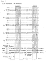
- the voltage waveforms of the data signals supplied by the X driver 250 in the second embodiment are as shown in Fig. 13. That is, a lighting voltage is applied in the second half time period and the first half time period in accordance with the fact that the selection voltage of the scanning signal is applied in the second half time period to the scanning lines 312 on the odd-numbered lines, and is applied in the first half time period to the scanning lines 312 on the subsequent even-numbered lines.
- the voltage switching frequency of the data signal Xp included in the display region and the voltage switching frequency of the data signal Xp included in the non-display region will be studied with reference to Fig. 14.
- the voltage switching frequency of the data signal Xp is, when the OFF (white)-displayed or ON (black)-displayed pixels continue in the column direction, 5 times per 4 horizontal scanning time periods 4H in which the scanning lines having the same polarity of the selection voltage are selected.
- the voltage switching frequency of the data signal Xp to the data lines 212 belonging to the display region is (m+1) times per m-horizontal scanning time periods mH if the OFF (white)-displayed or ON (black)-displayed pixels continue in the column direction, and it is understood that the voltage switching frequency is decreased as compared with the modification of the first embodiment (see Fig. 11 ). For this reason, in the second embodiment, it is possible to further reduce the power consumption, as compared with the first embodiment.
- the voltage switching frequency of the data signal Xp to the OFF (white)-displayed or ON (black)-displayed pixels can be decreased as compared with the first embodiment
- the voltage switching frequency of the data signal Xp to the gray-displayed pixels is 11 times per 4 horizontal scanning time periods 4H in this embodiment, and is, in general, when the polarity reversal period of the selection voltage is set to m-horizontal scanning time periods, (3m-1) times per m-horizontal scanning time periods mH, which is rather high as compared with the first embodiment.
- the gray display which remarkably consumes the power, need not be performed, and not only the voltage switching frequency of the data signal Xq to the non-display region but also the voltage switching frequency of the data signal Xp to the OFF (white)-displayed or ON (black)-displayed pixels in the display region is decreased, so that it is possible to further reduce the power consumption.
- a display device according to a third embodiment of the present invention will be described, but a general driving method when performing a gray scale display will be described before describing the display device.
- the method for the gray scale display is roughly divided into a voltage modulation and a pulse-width modulation, and a voltage for displaying a predetermined gray scale is difficult to be controlled according to the former voltage modulation, so that the latter pulse-width modulation is generally employed.
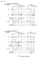
- the pulse-width modulation is applied to the above-described four-valued driving method (1/2H select), there are three types of modulation methods: a so-called rightward modulation method, as shown in Fig.
- the lighting voltage means, as described above, one of the data voltages applied to the data lines 212 which has the polarity opposite to that of the selection voltage in the time period in which the selection voltages ⁇ V S are applied, and means a voltage which contributes to the wiring of the pixel 116.
- the rightward modulation method shown in Fig. 15 (a) is generally employed in the four-valued driving method.
- the voltage switching frequency of the data signal Xp corresponding to the column is, if the polarity reversal period of the selection voltage is set to m-horizontal scanning time periods mH (m is an integer greater than 2), (2m-1) times per m-horizontal scanning time periods mH in the first and second embodiments, and the voltage scanning time period can be sufficiently brought closer to once per 1 horizontal scanning time period by increasing the value of m.
- the voltage switching frequency of the data signal Xp corresponding to the column is (3m-1) times, which is rather apt to increase, per m-horizontal scanning time periods mH in the second embodiment, as shown in Fig. 14. For this reason, if the ratio of the gray-displayed pixels in the display region of the partial display is increased, the voltage switching frequency of the data signal Xp increases, and the effect of decreasing the voltage switching frequency of the data signal Xq included in the non-display region is cancelled.
- the rightward modulation method is employed when the selection voltage is applied in the second half time period 1/2H of 1 horizontal scanning time period
- the leftward modulation method is employed when the selection voltage is applied in the first half time period of the 1 horizontal scanning method, so that the lighting voltage is continuously applied in the second half time period and the first half time period, and the voltage switching frequency of the data signal Xp concerning the gray display is limited to a low level.
- this display device differs from the display device of the second embodiment only in the control signal on the X-side, and the mechanical and electrical configurations are the same as in the second embodiment. For this reason, as regards the third embodiment, a portion different from that of the second embodiment will be mainly described.
- the logical level of the alternate current driving signal MY is set so as to be reversed every 4 horizontal scanning time periods 4H in which four scanning lines 312 are selected such that the 1st line to the 4th line, the 5th line to the 8th line, the 9th line to the 12th line, ..., the 197th line to the 200th line.
- a control signal INH has twice the period of a clock signal YCLK, and is set to be at an H-level over the second half time period of the 1 horizontal scanning time period in which scanning lines 312 on the odd-numbered lines are selected and the first half time period of the 1 horizontal scanning time period in which subsequent scanning lines 312 on the even-numbered lines are selected.
- the selection voltage of the scanning signal is applied in the second half time period of the 1 horizontal scanning time period 1H in which the scanning lines are selected, and as regards the scanning lines 312 on the subsequent even-numbered lines, the selection voltage of the scanning signal is applied in the first half time period of the 1 horizontal scanning time period 1H. This point is the same as the second embodiment.
- the alternate current driving signal MX on the X-side is the same as the second embodiment. That is, it is common to the first embodiment that the logical level of the alternate current driving signal MX is obtained by reversing the level of the alternate current driving signal MY when the control signal INH is at the H-level, while the logical level is obtained by maintaining the level of the alternate current driving signal MY when the control signal INH is at the L-level, but since the alternate current driving signal MY and the control signal INH are changed in the third embodiment as described above, the alternate current driving signal MX is changed according thereto.
- a latch pulse LPc is supplied in place of the latch pulse LPb in the second embodiment and further, a gray scale code pulse GCPR for rightward modulation and a gray scale code pulse GCPL for leftward modulation are supplied in place of the gray scale code pulse GCP to the PWM decoder 2506 (see Fig. 8) in the X driver 250.
- the latch pulse LPc is obtained by extracting a latch pulse outputted at the time of changing the logical level of the alternate current driving signal MY from the latch pulse LP for defining a start of the 1 horizontal scanning time period 1H, as shown in Fig. 16.
- the gray scale code pulse for rightward modulation GCPR is a gray scale controlling pulse used in the rightward modulation method arranged at the position of the time period on the proximal side from each of the end points of the first half time period and the second half time period, into which the 1 horizontal scanning time period 1H is divided, according to the level of the intermediate gray scale, as shown in Fig. 16, and is the same as the gray scale code pulse GCP in the first and second embodiments.
- the gray scale code pulse GCPL for leftward modulation is a gray scale controlling pulse used in the leftward modulation method, and is arranged at the position of the time period corresponding to level of the intermediate gray scale from each of the starting points of the first half time period and the second half time period of the 1 horizontal scanning time period 1H, as shown in Fig. 16.
- a PWM decoder 2506 in the third embodiment generates the following voltage selection signal using the signals, such as the latch pulse LPc, the gray scale code pulse GCPR for the rightward modulation, and the gray scale code pulse GCPL for the leftward modulation.
- the PWM decoder 2506 first, when the latch pulse LP supplied simultaneously with the latch pulse LPc is assumed to be the 1st latch pulse, recognizes a time period during which the 2nd latch pulse LP is supplied after the 1st latch pulse LP is supplied, and a time period during which the 4th latch pulse LP is supplied after the 3rd latch pulse LP is supplied as 1 horizontal scanning time period, respectively, in which a selection voltage should be supplied in the second half time period, while the PWM decoder 2506 recognizes a time period during which the 3rd latch pulse LP is supplied after the 2nd latch pulse LP is supplied, and a time period during which the next latch pulse LP is supplied after the 4th latch pulse LP is supplied as 1 horizontal scanning time period, respectively, in which the selection voltage should be supplied in the first half time period.
- the PWM decoder 2506 when the 1 horizontal scanning time period is recognized in which the selection voltage should be supplied in the second half time period, pays attention to one gray scale data Dn, and if the gray scale data designates an intermediate gray scale (gray) display other than the ON display and the OFF display, generates a voltage selection signal corresponding thereto so that, second, the polarity of the signal is reset to the same polarity as that represented by an immediately preceding logical level of an alternate current driving signal MX at the rising edge of the latch pulse LP, third, the polarity of the signal is set to the same polarity as that represented by the logical level of the alternate current driving signal MX at the falling edge of one of the gray scale code pulses GCPR for the rightward modulation in the first half time period corresponding to the gray scale data Dn, and fourth, the polarity of the signal is set again to the same polarity as that represented by the logical level of the alternate current driving signal MX at the falling edge of one of the gray scale code pulses
- the PWM decoder 2506 when the 1 horizontal scanning time period is recognized in which the selection voltage should be supplied in the first half time period, pays attention to one gray scale data Dn, and if the gray scale data designates the intermediate gray scale (gray) display other than the ON display and the OFF display, generates a voltage selection signal corresponding thereto so that, second, the polarity of the signal is reset to the same polarity as that represented by the logical level of the alternate current driving signal MX at the rising edge of the latch pulse LP, third, the polarity of the signal is set to be opposite to the polarity represented by the logical level of the alternate current driving signal MX at the falling edge of one of the gray scale code pulses GCPL for leftward modulation in the first half time period corresponding to the gray scale data Dn, and fourth, the polarity of the signal is set again to be opposite to the polarity represented by the logical level of the alternate current driving signal MX at the falling edge of one of the gray scale code pulses GCPR
- the PWM decoder 2506 generates the voltage selection signal using the reset signal RES and the like so that, if the gray scale data Dn is (00) corresponding to the OFF (white) display, the polarity of the signal is opposite to the polarity represented by the logical level of the alternate current driving signal MX, and that, if the gray scale data Dn is (11) corresponding to the ON (black) display, the signal has the polarity represented by the logical level of the alternate current driving signal MX.
- the voltage waveforms of the data signal supplied to the X driver 250 in the third embodiment are as shown in Fig. 16. That is, when the selection voltage is applied to a certain scanning line 312 in the second half time period, the lighting voltage is applied by the rightward modulation method, and when the selection voltage is applied to a subsequent scanning line 312 in the first half time period, the lighting voltage is applied by the leftward modulation method, so that the lighting voltage is applied continuously in the second half time period and the first half time period.
- the frequency when the voltage switching frequency of the data signal Xp to the gray-displayed pixel included in the display region is studied, the frequency is 9 times per 4 horizontal scanning time periods 4H, and in general, in the case where the polarity reversal period of the selection voltage is set to m-horizontal scanning time periods, the frequency is (2m+1) times per m-horizontal scanning time periods mH, which is the same as the first embodiment.
- the voltage switching frequency of the data signal Xp is 5 times per the 4 horizontal scanning time periods 4H in which the scanning lines having the same polarity of the selection voltage are selected, and in general, when the polarity reversal period of the selection voltage is set to m-horizontal scanning time periods, the voltage switching frequency of the data signal Xp to the data lines 212 belonging to the display region is (m+1) times per m-horizontal scanning time periods mH.
- the voltage switching frequency of the data signal Xp to the OFF (white)-displayed or ON (black)-displayed pixels included in the display region can be limited to the same level as the second embodiment and further, the voltage switching frequency of the data signal Xp to the gray-displayed pixels can be limited to the same level as the first embodiment.
- m representing the polarity reversal period of the selection voltage tends to be regarded as an even number greater than 2, but m may be an odd number.
- m is an odd number, unpaired horizontal scanning time periods are generated, but they do not affect the voltage switching frequency of the data signals Xp and Xq.
- the data PDx for specifying the data line 212 presenting the non-display is supplied to the PWM decoder 2506 in the above-described embodiments
- a configuration may be adopted in which the data PDx is supplied to the address control circuit 2502 so as to inhibit the generation of the read address Rad of the gray scale data Dn corresponding to the data, and whereby, the PWM decoder 2506 recognizes that the data lines from which the gray scale data Dn is not read should present non-display, and generates the voltage selection signal of the data signal Xq.
- the transmissive display device is described in the above embodiments, a reflective or a transflective display device may also be employed.
- the pixel electrodes 234 may be formed of a reflective metal, such as aluminum, or a reflective film may be separately formed so that light from the counter substrate 300 is reflected.
- the transflective display device is employed, the pixel electrode 234 formed of reflective metal or the reflective film may be formed very thin, or an opening may be provided, and when the reflective display device is employed, light from the counter substrate 300 is reflected, while illuminating light generated by the backlight may be transmitted when the transmissive display device is employed.
- the present invention is not limited thereto, and a multi-gray scale display presented by 3 bits or more may be performed.
- the pixels may be allowed to correspond to red (R), green (G), and blue (B) so as to perform color display.
- Fig. 1 while the TFD 220 is connected to the side of the data line 212 and the liquid crystal layer 118 is connected to the side of the scanning line 312, contrary to this, the TFD 220 may be connected to the side of the scanning line 312, and the liquid crystal layer 118 may be connected to the side of the data line 212.
- the TFD 220 in the above-described liquid crystal panel 100 is an example of switching device, and a device using ZnO (zinc oxide) variable resistor or an MSI (Metal Semi-Insulator), and a tow-terminal device can be applied in which two devices are connected in series or in parallel in the opposite direction and further, a three-terminal device can be applied, such as an insulating gate field effect transistor.
- ZnO zinc oxide
- MSI Metal Semi-Insulator
- both the data lines 212 and the scanning lines 312 should be formed on the device substrate 200 in such a manner as to intersect with one another, instead of forming only the data lines or only the scanning lines 312 thereon, such an application is disadvantageous in that the likelihood of occurrence of a short circuit in the wiring is enhanced, and that the manufacturing process is complicated because the configuration of a TFT itself is more complicated than that of a TFD.
- the display device of the present invention is applicable to a passive-type liquid crystal, which does not employ a switching device, such as a TFD or a TFT.
- liquid crystal of a bi-stable type having memory such as a BTN (Bi-stable Twisted Nematic) type/ferroelectric type, a polymer dispersed type and further, a GH (guest-host) type in which a dye (guest) having anisotropy in the absorption of visible light in the major axis and the minor axis of molecules is dissolved in a liquid crystal (host) having a fixed molecular arrangement, and the dye molecules and the liquid-crystal molecules are arranged in parallel, may be employed.
- BTN Bi-stable Twisted Nematic
- GH guest-host
- perpendicular orientation (homeotropic orientation) may be adopted in which the liquid-crystal molecules are perpendicularly arranged with respect to the two substrates when no voltage is applied, while the liquid-crystal modulates are arranged in parallel to the two substrates with a voltage applied
- parallel (horizontal) orientation (homogeneous orientation) may be adopted in which the liquid-crystal molecules are arranged in parallel to the two substrates when no voltage is applied, while the molecules are perpendicularly arranged to the two substrates when a voltage is applied.
- the present invention is applicable to a display device for performing a display by utilizing the electro-optical effect, such as an electroluminescent device, a fluorescent display tube, and a plasma display. That is, the present invention is applicable to all display devices each having a configuration similar to that of the above-described display device.
- a computer 1100 includes a main body portion 1104 provided with a keyboard 1102, and a liquid crystal panel 100 used as a display portion.
- a backlight is provided on the back face of the liquid crystal panel 100 to improve visibility, the backlight is omitted in the figure because it is not seen outwardly.
- a portable telephone 1200 includes the above-described liquid crystal panel 100, in addition to a plurality of operating buttons 1202, an earpiece 1204, and a mouthpiece 1206.
- This liquid crystal panel 100 performs a full-screen display using all regions as display regions at the time of reception or transmission, while the liquid crystal panel 100 performs partial display at the time of waiting for incoming calls, and displays only necessary information, such as electric field strength, numbers, characters, and date and time, on the display region.
- FIG. 25 is a perspective view showing the configuration of this digital still camera, but the figure also shows simply an interfacing to external apparatuses.
- a normal silver salt camera exposes a film to the light by an optical image of an object
- a digital still camera 1300 subjects the optical image of the object to an photoelectric conversion by an image pickup device, such as a CCD (Charge Coupled Device), to generate an image pickup signal.
- an image pickup device such as a CCD (Charge Coupled Device)
- the above-described liquid crystal panel 100 is provided on the back face of a case 1302 of the digital still camera 1300, and a display is performed on the basis of the image pickup signals generated by the CCD. For this reason, the liquid crystal panel 100 functions as a viewfinder for displaying the object.
- a light-receiving unit 1304 including an optical lens, the CCD, and the like is provided on the side of a front surface (on the rear face in Fig. 25) of the case 1302.
- a photographer confirms an object image displayed on the liquid crystal panel 100, and presses down a shutter button 1306, image pickup signals of the CCD at that time are transferred to and stored in a memory of a circuit board 1308.
- a video signal output terminal 1312 and a data communicating input/output terminal 1314 are provided on a side surface of the case 1302.
- a television monitor 1320 is connected to the former video signal output terminal 1312
- a personal computer 1330 is connected to the latter data communication input/output terminal 1314 according to demand.
- the image pickup signals stored in the memory of the circuit board 1308 are outputted to the television monitor 1320 and the personal computer 1330 by a predetermined operation.
- a liquid crystal television set in addition to the personal computer shown in Fig. 23, the portable telephone shown in Fig. 24, and the digital still camera shown in Fig. 25, a liquid crystal television set, a viewfinder-type or monitor direct view-type video tape recorder, a car navigation system, a pager, an electronic notepad, an electric calculator, a word processor, a workstation, a television telephone, a POS terminal, and an apparatus having a touch panel are cited as examples of the electronic apparatus. And, it is needless to say that the above-described display device is applicable to a display portion of the various types of the electronic apparatuses.
- a switching frequency of a voltage is decreased, as compared with a case where a non-selection voltage is simply applied to the data lines other than the specific data line, so that the power consumed in accordance with the switching of the voltage can be limited to a low level.
Landscapes
- Engineering & Computer Science (AREA)
- Chemical & Material Sciences (AREA)
- Crystallography & Structural Chemistry (AREA)
- Physics & Mathematics (AREA)
- Computer Hardware Design (AREA)
- General Physics & Mathematics (AREA)
- Theoretical Computer Science (AREA)
- Liquid Crystal Display Device Control (AREA)
- Control Of Indicators Other Than Cathode Ray Tubes (AREA)
- Liquid Crystal (AREA)
Abstract
Description
Claims (11)
- A method for driving a display device driving a pixel provided corresponding to each of intersections between a plurality of scanning lines and a plurality of data lines, wherein one scanning line in said plurality of scanning lines is selected every 1 horizontal scanning time period, and a selection voltage is applied to the selected scanning line in one of time periods, into which the 1 horizontal scanning time period is divided; the polarity of said selection voltage is reversed at least every two or more horizontal scanning time periods on the basis of an intermediate value of a lighting voltage and a non-lighting voltage applied to said data lines; when a pixel belonging to a specific data line in said plurality of data lines is put into a display state, and pixels belonging to other data lines are put into a non-display state, a lighting voltage is applied to said specific data line in 1 horizontal scanning time period, in which one scanning line in said plurality of scanning lines is selected and a selection voltage is applied to the selected scanning line, according to the contents to be displayed by a pixel corresponding to an intersection between the selected scanning line and the specific data line, and a lighting voltage and a non-lighting voltage are applied to said specific data line for substantially the same period over 1 horizontal scanning time period, in which the selected scanning line is selected, while a non-lighting voltage is supplied to data lines other than said specific data line according to the polarity of the selection voltage applied to the selected scanning line, and by reversing the polarity every polarity reversal period of said selection voltage.
- The method for driving a display device as claimed in Claim 1, wherein, when an scanning line is selected, a selection voltage is applied to the selected scanning line in the second half time period of one of time periods, into which 1 horizontal scanning time period is divided; when the next one scanning line is selected, a selection voltage is applied to the selected scanning line in the first half time period of one of time periods, into which 1 horizontal scanning time period is divided; and the selection voltage is alternately applied in one time period and in the other time period every 1 horizontal scanning time period.
- The method for driving a display device as claimed in Claim 2, wherein, when said selection voltage is applied in said second half time period, a lighting voltage is applied to said specific data line from a point of time before an end point of the second half time by a time period according to the gray scale of a pixel corresponding to an intersection between the selected scanning line and the specific data line to the end point of the second half time period, and a non-lighting voltage is applied in the remaining time period of the second half time period; while, when said selection voltage is applied in said first half time period, a lighting voltage is applied to said specific data line from a starting point of the first half time period to a time period according to the gray scale of a pixel corresponding to an intersection between the selected scanning line and the specific data line, and a non-lighting voltage is applied in the remaining time period of the first half time period.
- A driving circuit for a display device driving a pixel provided corresponding to each of intersections between a plurality of scanning lines and a plurality of data lines, the driving circuit comprising: a scanning line driving circuit for selecting one scanning line in said plurality of scanning lines every 1 horizontal scanning time period, applying a selection voltage to the selected scanning line in one of time periods, into which the 1 horizontal scanning time period is divided, and reversing the polarity of said selection voltage at least every two or more horizontal scanning time periods on the basis of an intermediate value of a lighting voltage and a non-lighting voltage applied to said data lines; and a data line driving circuit for applying, when a pixel belonging to a specific data line in said plurality of data lines is put into a display state, and pixels belonging to other data lines are put into a non-display state, a lighting voltage to said specific data line in 1 horizontal scanning time period, in which one scanning line in said plurality of scanning lines is selected and a selection voltage is applied to the selected scanning line, according to the contents to be displayed by a pixel corresponding to an intersection between the selected scanning line and the specific data line, and applying a lighting voltage and a non-lighting voltage to said specific data line for substantially the same period over 1 horizontal scanning time period, in which the selected scanning line is selected, while supplying a non-lighting voltage to data lines other than said specific data line according to the polarity of the selection voltage applied to the selected scanning line, and by reversing the polarity every polarity reversal period of said selection voltage.
- The driving circuit for a display device as claimed in Claim 4, wherein said scanning line driving circuit applies a selection voltage to the selected scanning line in the second half time period of one of time periods, into which 1 horizontal scanning time period is divided, when an scanning line is selected; applies a selection voltage to the selected scanning line in the first half time period of one of time periods, into which 1 horizontal scanning time period is divided, when the next one scanning line is selected; and applies the selection voltage alternately in one time period and in the other time period every 1 horizontal scanning time period.
- The driving circuit for a display device as claimed in Claim 5, wherein, when said selection voltage is applied in said second half time period by said scanning line driving circuit, said data line driving circuit applies a lighting voltage to said specific data line from a point of time before an end point of the second half time by a time period according to the gray scale of a pixel corresponding to an intersection between the selected scanning line and the specific data line to the end point of the second half time period, and applies a non-lighting voltage in the remaining time period of the second half time period; while, when said selection voltage is applied in said first half time period by said scanning line driving circuit, said data line driving circuit applies a lighting voltage to said specific data line from a starting point of the first half time period to a time period according to the gray scale of a pixel corresponding to an intersection between the selected scanning line and the specific data line, and applies a non-lighting voltage in the remaining time period of the first half time period.
- A display device having a pixel provided corresponding to each of intersections between a plurality of scanning lines and a plurality of data lines, said display device comprising: a scanning line driving circuit for selecting one scanning line in said plurality of scanning lines every 1 horizontal scanning time period, applying a selection voltage to the selected scanning line in one of time periods into which the 1 horizontal scanning time period is divided, and reversing the polarity of said selection voltage at least every two or more horizontal scanning time periods on the basis of an intermediate value of a lighting voltage and a non-lighting voltage applied to said data lines; and a data line driving circuit for applying, when a pixel belonging to a specific data line in said plurality of data lines is put into a display state, and pixels belonging to other data lines are put into a non-display state, a lighting voltage to said specific data line in 1 horizontal scanning time period, in which one scanning line in said plurality of scanning lines is selected and a selection voltage is applied to the selected scanning line, according to the contents to be displayed by a pixel corresponding to an intersection between the selected scanning line and the specific data line, and applying a lighting voltage and a non-lighting voltage to said specific data line for substantially the same period over 1 horizontal scanning time period, in which the selected scanning line is selected, while supplying a non-lighting voltage to data lines other than said specific data line according to the polarity of the selection voltage applied to the selected scanning line, and by reversing the polarity every polarity reversal period of said selection voltage.
- The display device as claimed in Claim 7, wherein said pixel includes a capacitative device consisting of a switching device and an electro-optical material, and when a selection voltage is applied to one scanning line, a switching device of the pixel belonging to the scanning line is put into a conductive state, and writing operation according to a lighting voltage applied to the corresponding data line is performed on the capacitative device corresponding to the switching device.
- The display device as claimed in Claim 8, wherein said switching device is a two-terminal switching device, and said pixel is constructed by series-connecting said two-terminal switching device and said capacitative device between a scanning line and a data line.
- The display device as claimed in Claim 9, wherein said two-terminal switching device has a conductor/insulator/conductor structure connected to said scanning line or said data line.
- An electronic apparatus comprising the display device as claimed in any one of Claims 7 to 10.
Applications Claiming Priority (2)
| Application Number | Priority Date | Filing Date | Title |
|---|---|---|---|
| JP2000220836 | 2000-07-21 | ||
| JP2000220836A JP3829597B2 (en) | 2000-07-21 | 2000-07-21 | Display device driving method, driving circuit, display device, and electronic apparatus |
Publications (2)
| Publication Number | Publication Date |
|---|---|
| EP1174853A2 true EP1174853A2 (en) | 2002-01-23 |
| EP1174853A3 EP1174853A3 (en) | 2002-12-11 |
Family
ID=18715369
Family Applications (1)
| Application Number | Title | Priority Date | Filing Date |
|---|---|---|---|
| EP01306150A Withdrawn EP1174853A3 (en) | 2000-07-21 | 2001-07-17 | Driving method for display device, driving circuit, display device, and electronic apparatus |
Country Status (6)
| Country | Link |
|---|---|
| US (1) | US6940484B2 (en) |
| EP (1) | EP1174853A3 (en) |
| JP (1) | JP3829597B2 (en) |
| KR (1) | KR100404486B1 (en) |
| CN (1) | CN1162737C (en) |
| TW (1) | TW519609B (en) |
Cited By (2)
| Publication number | Priority date | Publication date | Assignee | Title |
|---|---|---|---|---|
| CN110301001A (en) * | 2017-02-17 | 2019-10-01 | 株式会社半导体能源研究所 | Display device |
| CN111276107A (en) * | 2020-02-24 | 2020-06-12 | 成都京东方光电科技有限公司 | Array substrate, control method and display panel |
Families Citing this family (9)
| Publication number | Priority date | Publication date | Assignee | Title |
|---|---|---|---|---|
| KR100917324B1 (en) * | 2002-11-16 | 2009-09-11 | 엘지디스플레이 주식회사 | LCD for Mobile Phone |
| JP4487024B2 (en) * | 2002-12-10 | 2010-06-23 | 株式会社日立製作所 | Method for driving liquid crystal display device and liquid crystal display device |
| JP2005099524A (en) * | 2003-09-25 | 2005-04-14 | Seiko Epson Corp | Electro-optical device, driving circuit and driving method thereof, and electronic apparatus |
| JP4093232B2 (en) * | 2004-01-28 | 2008-06-04 | セイコーエプソン株式会社 | Electro-optical device, driving circuit for electro-optical device, driving method for electro-optical device, and electronic apparatus |
| KR20050104652A (en) * | 2004-04-29 | 2005-11-03 | 삼성에스디아이 주식회사 | Electron emission display device and driving method thereof |
| KR20060104222A (en) * | 2005-03-29 | 2006-10-09 | 삼성에스디아이 주식회사 | Driving device of electron emission display device and driving method thereof |
| US7755615B2 (en) * | 2006-12-18 | 2010-07-13 | Motorola, Inc. | Optical shuttered touchscreen and method therefor |
| TWI406159B (en) * | 2009-05-13 | 2013-08-21 | Chimei Innolux Corp | Touch panel and touch display device |
| JP5572486B2 (en) * | 2010-09-01 | 2014-08-13 | シャープ株式会社 | Information display device and information display method |
Family Cites Families (6)
| Publication number | Priority date | Publication date | Assignee | Title |
|---|---|---|---|---|
| US3883778A (en) * | 1973-12-03 | 1975-05-13 | Hitachi Ltd | Driving apparatus for display element |
| US5379050A (en) * | 1990-12-05 | 1995-01-03 | U.S. Philips Corporation | Method of driving a matrix display device and a matrix display device operable by such a method |
| JP3734537B2 (en) * | 1995-09-19 | 2006-01-11 | シャープ株式会社 | Active matrix liquid crystal display device and driving method thereof |
| JP3617206B2 (en) * | 1996-08-16 | 2005-02-02 | セイコーエプソン株式会社 | Display device, electronic apparatus, and driving method |
| WO2000016305A1 (en) * | 1998-09-10 | 2000-03-23 | Koninklijke Philips Electronics N.V. | Matrix display device |
| JP3925016B2 (en) * | 1999-11-19 | 2007-06-06 | セイコーエプソン株式会社 | Display device driving method, driving circuit thereof, display device, and electronic apparatus |
-
2000
- 2000-07-21 JP JP2000220836A patent/JP3829597B2/en not_active Expired - Lifetime
-
2001
- 2001-07-02 TW TW090116168A patent/TW519609B/en not_active IP Right Cessation
- 2001-07-17 EP EP01306150A patent/EP1174853A3/en not_active Withdrawn
- 2001-07-18 US US09/906,643 patent/US6940484B2/en not_active Expired - Fee Related
- 2001-07-19 KR KR10-2001-0043318A patent/KR100404486B1/en not_active Expired - Fee Related
- 2001-07-20 CN CNB011232447A patent/CN1162737C/en not_active Expired - Fee Related
Cited By (5)
| Publication number | Priority date | Publication date | Assignee | Title |
|---|---|---|---|---|
| CN110301001A (en) * | 2017-02-17 | 2019-10-01 | 株式会社半导体能源研究所 | Display device |
| US11176900B2 (en) | 2017-02-17 | 2021-11-16 | Semiconductor Energy Laboratory Co., Ltd. | Display device |
| US11735131B2 (en) | 2017-02-17 | 2023-08-22 | Semiconductor Energy Laboratory Co., Ltd. | Display device |
| US12125453B2 (en) | 2017-02-17 | 2024-10-22 | Semiconductor Energy Laboratory Co., Ltd. | Display device |
| CN111276107A (en) * | 2020-02-24 | 2020-06-12 | 成都京东方光电科技有限公司 | Array substrate, control method and display panel |
Also Published As
| Publication number | Publication date |
|---|---|
| JP3829597B2 (en) | 2006-10-04 |
| US6940484B2 (en) | 2005-09-06 |
| TW519609B (en) | 2003-02-01 |
| JP2002040978A (en) | 2002-02-08 |
| US20020015030A1 (en) | 2002-02-07 |
| CN1334549A (en) | 2002-02-06 |
| EP1174853A3 (en) | 2002-12-11 |
| CN1162737C (en) | 2004-08-18 |
| KR100404486B1 (en) | 2003-11-05 |
| KR20020014681A (en) | 2002-02-25 |
Similar Documents
| Publication | Publication Date | Title |
|---|---|---|
| JP3975915B2 (en) | Display device driving method, driving circuit, display device, and electronic apparatus | |
| JP3968931B2 (en) | Display device driving method, driving circuit thereof, display device, and electronic apparatus | |
| US6771240B2 (en) | Method of driving matrix type display apparatus, display apparatus and electronic equipment | |
| KR100431385B1 (en) | Method for driving display, driving circuit therefor, display and electronic apparatus | |
| JP3956748B2 (en) | Display device, driving circuit thereof, driving method thereof, and electronic apparatus | |
| CN1319040C (en) | Electrooptic device intermodulation distortion correcting method and circuit,electrooptic apparatus and electronic apparatus | |
| US6940484B2 (en) | Systems and methods for driving a display device | |
| KR100631228B1 (en) | Electro-optical device, driving circuit thereof, driving method thereof, and electronic apparatus using electro-optical device | |
| JP2003044015A (en) | Electro-optical devices and electronic equipment | |
| JP4507542B2 (en) | Electro-optical device, driving circuit and driving method thereof, and electronic apparatus | |
| JP2002196722A (en) | Matrix type display device, driving method thereof and electronic equipment | |
| JP3820897B2 (en) | Display device, driving circuit thereof, driving method thereof, and electronic apparatus | |
| JP4661049B2 (en) | Electro-optical device driving method, driving circuit thereof, electro-optical device, and electronic apparatus | |
| JP2003066922A (en) | Electro-optical devices and electronic equipment | |
| JP4517837B2 (en) | Electro-optical device drive circuit, electro-optical device, and electronic apparatus | |
| JP2005189269A (en) | Crosstalk correction method for electro-optical device, correction circuit thereof, electro-optical device, and electronic apparatus | |
| JP2002140046A (en) | Display device driving method, driving circuit thereof, display device, and electronic apparatus |
Legal Events
| Date | Code | Title | Description |
|---|---|---|---|
| PUAI | Public reference made under article 153(3) epc to a published international application that has entered the european phase |
Free format text: ORIGINAL CODE: 0009012 |
|
| AK | Designated contracting states |
Kind code of ref document: A2 Designated state(s): AT BE CH CY DE DK ES FI FR GB GR IE IT LI LU MC NL PT SE TR |
|
| AX | Request for extension of the european patent |
Free format text: AL;LT;LV;MK;RO;SI |
|
| PUAL | Search report despatched |
Free format text: ORIGINAL CODE: 0009013 |
|
| AK | Designated contracting states |
Kind code of ref document: A3 Designated state(s): AT BE CH CY DE DK ES FI FR GB GR IE IT LI LU MC NL PT SE TR |
|
| AX | Request for extension of the european patent |
Free format text: AL;LT;LV;MK;RO;SI |
|
| 17P | Request for examination filed |
Effective date: 20030430 |
|
| AKX | Designation fees paid |
Designated state(s): AT BE CH CY DE DK ES FI FR GB GR IE IT LI LU MC NL PT SE TR |
|
| 17Q | First examination report despatched |
Effective date: 20050331 |
|
| STAA | Information on the status of an ep patent application or granted ep patent |
Free format text: STATUS: THE APPLICATION IS DEEMED TO BE WITHDRAWN |
|
| 18D | Application deemed to be withdrawn |
Effective date: 20050811 |