EP1172934A2 - Schaltungsanordnung zum Schalten von induktiven Lasten - Google Patents
Schaltungsanordnung zum Schalten von induktiven Lasten Download PDFInfo
- Publication number
- EP1172934A2 EP1172934A2 EP01116419A EP01116419A EP1172934A2 EP 1172934 A2 EP1172934 A2 EP 1172934A2 EP 01116419 A EP01116419 A EP 01116419A EP 01116419 A EP01116419 A EP 01116419A EP 1172934 A2 EP1172934 A2 EP 1172934A2
- Authority
- EP
- European Patent Office
- Prior art keywords
- switch
- inductance
- diode
- current
- capacitor
- Prior art date
- Legal status (The legal status is an assumption and is not a legal conclusion. Google has not performed a legal analysis and makes no representation as to the accuracy of the status listed.)
- Withdrawn
Links
Images

Classifications
-
- H—ELECTRICITY
- H03—ELECTRONIC CIRCUITRY
- H03K—PULSE TECHNIQUE
- H03K17/00—Electronic switching or gating, i.e. not by contact-making and –breaking
- H03K17/08—Modifications for protecting switching circuit against overcurrent or overvoltage
- H03K17/081—Modifications for protecting switching circuit against overcurrent or overvoltage without feedback from the output circuit to the control circuit
- H03K17/0814—Modifications for protecting switching circuit against overcurrent or overvoltage without feedback from the output circuit to the control circuit by measures taken in the output circuit
-
- H—ELECTRICITY
- H03—ELECTRONIC CIRCUITRY
- H03K—PULSE TECHNIQUE
- H03K17/00—Electronic switching or gating, i.e. not by contact-making and –breaking
- H03K17/08—Modifications for protecting switching circuit against overcurrent or overvoltage
- H03K17/081—Modifications for protecting switching circuit against overcurrent or overvoltage without feedback from the output circuit to the control circuit
- H03K17/0814—Modifications for protecting switching circuit against overcurrent or overvoltage without feedback from the output circuit to the control circuit by measures taken in the output circuit
- H03K17/08142—Modifications for protecting switching circuit against overcurrent or overvoltage without feedback from the output circuit to the control circuit by measures taken in the output circuit in field-effect transistor switches
Definitions
- the invention relates to a circuit arrangement for switching of inductive loads with a first and a second Supply potential, a first semiconductor switch, the is connected to the second supply potential, one first inductance forming a load, which between the first semiconductor switch and the first supply potential and a parallel branch to the first inductor, which has a first diode, the cathode of which Supply potential is switched, compared to the other supply potential has a positive voltage.
- a circuit arrangement of the type mentioned is for example from “Nlickmann, Dieter: The great work book Electronics, Franzis-Verlag Kunststoff, 1989 ".
- the there Circuit arrangement shown is used to control a Relay coil through a transistor.
- a diode is with the Cathode to a positive pole of a voltage supply in parallel switched to a relay coil.
- Relays are with a relatively small repetition frequency switched. at Applications in which the switching frequency increases significantly however, the losses in the transistor increase sharply.
- On Application examples for this case are pulse width modulated Controls of inductive loads. Especially in a non-intermittent mode of operation, i.e.
- the object of the invention is therefore a circuit arrangement for switching inductive loads where the Power loss in the semiconductor switch is considerably lower.
- the circuit arrangement according to the invention is advantageous because the first semiconductor switch neither with Voltage increases due to an induced voltage on the first inductance still with the current through the Free-wheeling diode is loaded.
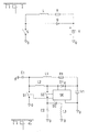
- FIG. 1 shows a circuit arrangement for switching inductive loads, as known from the prior art is.
- the principle of the circuit arrangement cited at the beginning this corresponds to switching a relay coil Circuitry.
- a switch S is generally as Switch shown; in use cases where the If the present invention is of interest, this becomes a Be semiconductor switches, for example a MOS transistor.
- An inductive load is characterized by an inductance L and a Resistor R shown, the usual series equivalent circuit diagram for an inductive load. Coils, equal what kind, always have an inductive and one resistive portion, the resistive portion in most Cases can be neglected.
- a voltage is induced at the inductance L. Without the diode D causes the voltage to steep Voltage increase at switch S, causing damage to it can.
- switches S so it is designed as a semiconductor switch, high losses.
- the diode D With its cathode to the Positive pole of the power supply is switched Electricity derived. If the switch S becomes conductive before the inductance L has discharged through the diode D, lies a so-called non-intermittent mode of operation. In this In this case, the switch S must be next to the actual load current through L the current currently flowing in the freewheeling diode D. take over, the full operating voltage and the Clearance current of the freewheeling diode D at the same time switch S strain. The losses increase the Junction temperature, for example one as switch S used MOS transistor, and influence this also the losses during the leading phase of switch S are negative.
- FIG. 2 shows a circuit arrangement according to the Invention is executed.
- a semiconductor switch S1 in non-intermittent mode of operation largely freed from switch-on losses.
- This is in Row to a free-wheeling diode D1 a second inductor L2 connected.
- This inductance L2 decouples the switch S1 and the diode D1 such that voltage jumps, but none Current jumps in switch S1 and in diode D1 are possible.
- This inductance L2 is comparatively small compared to that Load inductance L1.
- a capacitor C2 and the inductor L3 are connected at the junction of the second inductor L2 and the Diode D1 .
- the capacitor C2 and the inductor L3 are located on the other hand at the reference potential, which is the second Represents supply potential.
- a control unit SE which Voltage across the freewheeling diode D1 and the switching state of the evaluates the first switch S1 and on this basis the Switch S2 controls.
- the Switch S2 semi-synchronized with switch S1 in this way controlled that S2 becomes conductive when S1 is off and that S2 remains conductive until the current through the freewheeling diode D1 - coming from high values - has become almost zero because of the Current in the inductors L2 and L2 is almost the same size.
- the second and third inductors L2 and L3 are approximately same size, because with this self-control the required Energy for the second inductance L2 only in Short-term memory L3 and then in long-term memory C2 is saved.
- the proportion of C2 is low because it is on the operating voltage is clamped and this is relatively small against the amount of negative charging voltage. His share essentially covers the losses.
- This control of the second switch S2 therefore fits the energy requirements for the second inductance L2 automatically to a pulse width modulated Control from the first switch S1 on.
- first switch S1 If the first switch S1 is turned on again, becomes the connection point of the first inductor L1 to second inductance L2 and the first switch S1 Reference potential laid.
- the arrangement C1 commutates the stored energy, for example, in the main energy source back and the current in the second inductor L2 and through the freewheeling diode D1 goes linearly towards zero, since with constant voltage is commutated. To the same extent the current in S1 increases linearly from zero to the current in Load path.
- the diode D1 When the diode D1 is de-energized, the Tension on it at reference potential and a new cycle starts.
- FIG. 3 shows current and voltage profiles of the Circuit arrangement of Figure 2, the understanding of Serve circuit. It is clear that the negative to Reference potential charged capacitor C2 an essential higher voltage amount than the supply voltage U1 having.
- the first switch S1 blocks. simultaneously the second switch S2 becomes conductive, so that the Capacitor C2 can discharge into the second inductor L2.
- the voltage changes between t1 and t2 across capacitor C2 from negative bias to Zero.
- the current through L2 increases in a cosine shape on.
- the current maximum is through the second Inductance reached L2 and all the energy of the Capacitor C2 is transferred.
- the second inductor L2 now takes over the load inductance L1 flowed load current.
- the components are dimensioned so that the transition is very smooth.
- the current through L2 branches and partly flows through the diode D1 and to another part via the diode D2 in the third Inductance L3.
Landscapes
- Electronic Switches (AREA)
Abstract
Description
- Figur 1
- eine Schaltungsanordnung aus dem Stand der Technik,
- Figur 2
- ein Ausführungsbeispiel einer erfindungsgemäßen Schaltungsanordnung und
- Figur 3
- Strom- und Spannungsverläufe der Schaltungsanordnung von Figur 2.
Claims (2)
- Schaltungsanordnung mitdadurch gekennzeichnet, daßeinem ersten und einem zweiten Versorgungspotential (U1, 0),einem ersten Halbleiterschalter (S1), der mit dem zweiten Versorgungspotential (0) verbunden ist,einer ersten eine Last bildenden Induktivität (L1), die zwischen dem ersten Halbleiterschalter (S1) und dem ersten Versorgungspotential (U1) liegt,einem Parallelzweig zu der ersten Induktivität (L1), der eine erste Diode (D1) aufweist, deren Kathode (K) zu dem Versorgungspotential (U1) geschaltet ist, das gegenüber dem anderen Versorgungspotential (0) eine positive Spannung aufweist,der Parallelzweig eine zweite Induktivität (L2) aufweist, die in Reihe zu der ersten Diode (D1) geschaltet ist und mit dem Verbindungspunkt der ersten Induktivität (L1) mit dem ersten Schalter (S1) verbunden ist,an der Verbindungsstelle zwischen der ersten und der zweiten Induktivität (L1, L2) eine erste kapazitive Anordnung (C1) angekoppelt ist, die mit dem zweiten Versorgungspotential (0) verbunden ist,an der Verbindungsstelle zwischen der zweiten Induktivität (L2) und der ersten Diode (D1) ein zweiter Halbleiterschalter (S2) angeschlossen ist, der über eine Anordnung, die eine zweite Kapazität (C2) und parallel dazu eine Reihenschaltung aus einer zweiten Diode (D2) und einer dritten Induktivität (L3) aufweist, mit dem zweiten Versorgungspotential (0) verbunden ist, undeiner Steuereinheit (SE), die den zweiten Schalter (S2) halbsynchron mit dem ersten Schalter (S1) derart steuert, daß der zweite Schalter (S2) leitend wird, wenn der erste Schalter (S1) sperrt, und leitend bleibt, bis der Strom durch die erste Diode (D1) einen vorbestimmten Schwellwert nahe Null unterschreitet.
- Schaltungsanordnung nach Anspruch 1,
dadurch gekennzeichnet, daß die zweite und die dritte Induktivität (L2, L3) gleich groß sind.
Priority Applications (1)
| Application Number | Priority Date | Filing Date | Title |
|---|---|---|---|
| EP01116419A EP1172934A3 (de) | 2000-07-12 | 2001-07-06 | Schaltungsanordnung zum Schalten von induktiven Lasten |
Applications Claiming Priority (3)
| Application Number | Priority Date | Filing Date | Title |
|---|---|---|---|
| EP00114878 | 2000-07-12 | ||
| EP00114878 | 2000-07-12 | ||
| EP01116419A EP1172934A3 (de) | 2000-07-12 | 2001-07-06 | Schaltungsanordnung zum Schalten von induktiven Lasten |
Publications (2)
| Publication Number | Publication Date |
|---|---|
| EP1172934A2 true EP1172934A2 (de) | 2002-01-16 |
| EP1172934A3 EP1172934A3 (de) | 2006-06-07 |
Family
ID=26071145
Family Applications (1)
| Application Number | Title | Priority Date | Filing Date |
|---|---|---|---|
| EP01116419A Withdrawn EP1172934A3 (de) | 2000-07-12 | 2001-07-06 | Schaltungsanordnung zum Schalten von induktiven Lasten |
Country Status (1)
| Country | Link |
|---|---|
| EP (1) | EP1172934A3 (de) |
Family Cites Families (2)
| Publication number | Priority date | Publication date | Assignee | Title |
|---|---|---|---|---|
| GB1262478A (en) * | 1968-12-23 | 1972-02-02 | Lucas Industries Ltd | Thyristor circuits |
| US4365171A (en) * | 1980-12-23 | 1982-12-21 | General Electric Company | Low loss snubber circuit |
-
2001
- 2001-07-06 EP EP01116419A patent/EP1172934A3/de not_active Withdrawn
Also Published As
| Publication number | Publication date |
|---|---|
| EP1172934A3 (de) | 2006-06-07 |
Similar Documents
| Publication | Publication Date | Title |
|---|---|---|
| DE10315982B4 (de) | Schaltungsanordnung für ein hybrides Schütz | |
| EP0108283B1 (de) | Elektronischer Schalter | |
| DE102006029475B4 (de) | Effiziente Einschaltstrom-Begrenzungsschaltung mit bidirektionellen Doppelgate-HEMT-Bauteilen | |
| DE10046668B4 (de) | Elektrische Lastansteuerungsschaltung mit Schutzeinrichtung | |
| DE102015112245B4 (de) | Gleichrichter | |
| DE19746112A1 (de) | Stromrichteranordnung | |
| EP2907152A1 (de) | Vorrichtung zum schalten eines gleichstromes in einem pol eines gleichspannungsnetzes | |
| DE4413546A1 (de) | Gleichstrom-Steuerschaltung | |
| DE2644715C2 (de) | Einrichtung zur Befreiung elektrischer oder elektronischer Einwegschalter von hoher Verlustleistungsbeanspruchung während des Einschaltens - bei welchem ein, zuvor in einem anderen Schaltungspfad fließender, von Null verschiedener Strom auf den betreffenden Einwegschalter überwechselt - und von überhöhter Sperrspannungsbeanspruchung zum Ende des Ausschaltens | |
| DE4421249C2 (de) | Schaltstromversorgungsgerät mit Snubber-Schaltung | |
| DE3931729C1 (de) | ||
| EP2992598A1 (de) | Hoch- oder tiefsetzsteller mit entlastungskondensator | |
| DE3241086A1 (de) | Anordnung zur verlustmindernden nutzung der in einem entlastungsnetzwerk gespeicherten elektrischen energie | |
| DE2555168C2 (de) | Schaltungsanordnung für einen Schalttransistor | |
| DE3743437C1 (en) | Low-loss, three-point invertor which is relieved of switching loads | |
| EP1366502B1 (de) | Elektrische schaltung zur vermeidung eines lichtbogens über einem elektrischen kontakt | |
| DE102019107112B3 (de) | Schaltvorrichtung, Spannungsversorgungssystem, Verfahren zum Betreiben einer Schaltvorrichtung und Herstellverfahren | |
| DE10103633A1 (de) | Leistungselektronischer Drosselwandler zur Spannungsanpassung | |
| EP1429461A1 (de) | Getaktete Leistungsversorgung | |
| DE2716367C2 (de) | Schutzbeschaltung für im Wechselschaltbetrieb gegen induktive Last arbeitende Transistoren | |
| EP1172934A2 (de) | Schaltungsanordnung zum Schalten von induktiven Lasten | |
| EP1195885B1 (de) | Synchrongleichrichterschaltung | |
| EP1521354A2 (de) | Synchrongleichrichter | |
| EP0009225A1 (de) | Schutzbeschaltung | |
| DE3872434T2 (de) | Symmetrische elektrische daempferschaltung. |
Legal Events
| Date | Code | Title | Description |
|---|---|---|---|
| PUAI | Public reference made under article 153(3) epc to a published international application that has entered the european phase |
Free format text: ORIGINAL CODE: 0009012 |
|
| AK | Designated contracting states |
Kind code of ref document: A2 Designated state(s): AT BE CH CY DE DK ES FI FR GB GR IE IT LI LU MC NL PT SE TR |
|
| AX | Request for extension of the european patent |
Free format text: AL;LT;LV;MK;RO;SI |
|
| PUAL | Search report despatched |
Free format text: ORIGINAL CODE: 0009013 |
|
| AK | Designated contracting states |
Kind code of ref document: A3 Designated state(s): AT BE CH CY DE DK ES FI FR GB GR IE IT LI LU MC NL PT SE TR |
|
| AX | Request for extension of the european patent |
Extension state: AL LT LV MK RO SI |
|
| AKX | Designation fees paid | ||
| REG | Reference to a national code |
Ref country code: DE Ref legal event code: 8566 |
|
| STAA | Information on the status of an ep patent application or granted ep patent |
Free format text: STATUS: THE APPLICATION IS DEEMED TO BE WITHDRAWN |
|
| 18D | Application deemed to be withdrawn |
Effective date: 20061208 |