EP1172865A2 - Semiconductor photosensitive device - Google Patents
Semiconductor photosensitive device Download PDFInfo
- Publication number
- EP1172865A2 EP1172865A2 EP01116841A EP01116841A EP1172865A2 EP 1172865 A2 EP1172865 A2 EP 1172865A2 EP 01116841 A EP01116841 A EP 01116841A EP 01116841 A EP01116841 A EP 01116841A EP 1172865 A2 EP1172865 A2 EP 1172865A2
- Authority
- EP
- European Patent Office
- Prior art keywords
- type semiconductor
- conductivity type
- semiconductor layer
- wavelength
- light
- Prior art date
- Legal status (The legal status is an assumption and is not a legal conclusion. Google has not performed a legal analysis and makes no representation as to the accuracy of the status listed.)
- Granted
Links
Images


Classifications
-
- H—ELECTRICITY
- H10—SEMICONDUCTOR DEVICES; ELECTRIC SOLID-STATE DEVICES NOT OTHERWISE PROVIDED FOR
- H10F—INORGANIC SEMICONDUCTOR DEVICES SENSITIVE TO INFRARED RADIATION, LIGHT, ELECTROMAGNETIC RADIATION OF SHORTER WAVELENGTH OR CORPUSCULAR RADIATION
- H10F30/00—Individual radiation-sensitive semiconductor devices in which radiation controls the flow of current through the devices, e.g. photodetectors
- H10F30/20—Individual radiation-sensitive semiconductor devices in which radiation controls the flow of current through the devices, e.g. photodetectors the devices having potential barriers, e.g. phototransistors
-
- H—ELECTRICITY
- H10—SEMICONDUCTOR DEVICES; ELECTRIC SOLID-STATE DEVICES NOT OTHERWISE PROVIDED FOR
- H10F—INORGANIC SEMICONDUCTOR DEVICES SENSITIVE TO INFRARED RADIATION, LIGHT, ELECTROMAGNETIC RADIATION OF SHORTER WAVELENGTH OR CORPUSCULAR RADIATION
- H10F30/00—Individual radiation-sensitive semiconductor devices in which radiation controls the flow of current through the devices, e.g. photodetectors
- H10F30/20—Individual radiation-sensitive semiconductor devices in which radiation controls the flow of current through the devices, e.g. photodetectors the devices having potential barriers, e.g. phototransistors
- H10F30/21—Individual radiation-sensitive semiconductor devices in which radiation controls the flow of current through the devices, e.g. photodetectors the devices having potential barriers, e.g. phototransistors the devices being sensitive to infrared, visible or ultraviolet radiation
- H10F30/24—Individual radiation-sensitive semiconductor devices in which radiation controls the flow of current through the devices, e.g. photodetectors the devices having potential barriers, e.g. phototransistors the devices being sensitive to infrared, visible or ultraviolet radiation the devices having only two potential barriers, e.g. bipolar phototransistors
Definitions
- the present invention relates to a semiconductor device, more particularly relates to a semiconductor device having a photo diode for receiving a plurality of light having different wavelengths.
- Light receiving elements that is, photo diodes
- photo diode there are several kinds of the above photo diode, but basically it is comprised of a pn junction of a semiconductor.
- a depletion layer spreads in a p-type semiconductor region and an n-type semiconductor region, respectively, from a pn-junction surface. Electron-hole pairs are generated by light absorbed mainly in the depletion layer. The electrons move to the n-type semiconductor region drawn by the electric field, while the holes move to the p-type semiconductor region and are detected as a current.
- an I layer (p - -layer or n - -layer) containing conductive impurities at a low concentration between the p-layer and n-layer, it is possible to have the depletion layer spread by a low voltage. This is called a PIN photo diode.
- Figure 1A is a sectional view of the above PIN photo diode.
- a p - -type semiconductor layer 11 is formed on the p + -type semiconductor substrate 10, furthermore, an n-type semiconductor layer 12 is formed at a surface region of the p - -type semiconductor layer 11 so that the pn junction is formed.
- a p + -type semiconductor layer 13 is formed to surround the PIN diode region. It becomes a take-out portion of a p-region and isolates the PIN diode region from other elements.
- a protective insulating film 14 comprised of silicon oxide etc. is formed at an upper layer of the n-type semiconductor layer 12 and the p + -type semiconductor layer 13. Contacts respectively reaching the n-type semiconductor layer 12 and the p + -type semiconductor layer 13 are opened, and take-out electrodes (15a and 15b) are formed.
- a depletion layer V spreads from the pn-junction surface to the directions of the p - -type semiconductor layer 11 and n-type semiconductor layer 12 as shown in Fig. 1B.
- the depletion layer V spreads so that the total number of carriers becomes equal at the n-side and p-side, so spreads more to the p - -type semiconductor layer 11 side having a low carrier concentration.
- a photo diode such as the above conventional PIN photo diode is normally designed to in structure optimized for light having a certain wavelength, for example, near 780 nm when used in a CD system and near 650 nm when used in a DVD system.
- a photo diode of the same structure there is a large wavelength dependence of the light receiving sensitivity, so when trying to receive a plurality of light having different wavelengths such as light of wavelengths of 780 nm and 650 nm by an identical photo diode or by a plurality of photo diodes of the same structure present on an identical substrate, the sensitivity ends up greatly differing at the different wavelengths.
- An object of the present invention is to provide a semiconductor device having a photo diode having substantially the same sensitivity for a plurality of light of different wavelengths.
- a semiconductor device of the present invention is a semiconductor device having a photo diode comprising a first conductivity type semiconductor layer and a second conductivity type semiconductor layer formed at a surface layer portion of said first conductivity type semiconductor layer, wherein the sensitivity of said photo diode to light of a first wavelength and the sensitivity to light of a second wavelength which is different from said first wavelength are made to become substantially the same by designing a region in which a depletion layer spreads from a junction surface of said first conductivity type semiconductor layer and said second conductivity type semiconductor layer when inverse biases are applied to said first conductivity type semiconductor layer and said second conductivity type semiconductor layer.
- the sensitivity of said photo diode to light of a first wavelength and the sensitivity to light of a second wavelength are made to become substantially the same by designing impurity concentrations and said inverse biases of said first conductivity type semiconductor layer and said second conductivity type semiconductor layer and by designing said region in which a depletion layer spreads.
- the depletion layer is designed to spread in a region including a region 3 to 6 ⁇ m or 2 to 7 ⁇ m in the depth direction from a surface of the second conductivity type semiconductor layer.
- the first conductivity type semiconductor layer is formed on a first conductivity type semiconductor substrate containing a first conductivity type impurity at a higher concentration than the first conductivity type semiconductor layer.
- the concentration of the first conductivity type impurity on the surface of the first conductivity type semiconductor substrate is at least 1 ⁇ 10 17 /cm 3 .
- a distance between an end face of said depletion layer on said first conductivity type semiconductor substrate side and the surface of said first conductivity type semiconductor substrate is 3 ⁇ m or less.
- said first wavelength is 780 nm and said second wavelength is 650 nm.
- a semiconductor device of the present invention is a semiconductor device comprising a first conductivity type semiconductor substrate, a first conductivity type semiconductor layer formed on a first conductivity type semiconductor substrate and containing a first conductivity type impurity at a lower concentration than said first conductivity type semiconductor substrate, and a second conductivity type semiconductor layer formed at a surface layer portion of said first conductivity type semiconductor layer, wherein a photo diode is formed by spreading a depletion layer from a junction surface of said first conductivity type semiconductor layer and said second conductivity type semiconductor layer when inverse biases are applied to said first conductivity type semiconductor layer and said second conductivity type semiconductor layer, and the concentrations of the impurity of said first and second conductivity layers are adjusted so that the depletion layer spreading region is made wherein the sensitivity of said photo diode to light of a first wavelength and the sensitivity to light of a second wavelength which is different from said first wavelength become substantially the same.
- the semiconductor device of the present invention is provided with a photo diode having a first conductivity type semiconductor layer and a second conductivity type semiconductor layer formed at a surface layer portion of said first conductivity type semiconductor layer, wherein the sensitivity to light of a first wavelength and the sensitivity to light of a second wavelength which is different from said first wavelength are made to become substantially the same by designing the impurity concentrations and said inverse biases of said first conductivity type semiconductor layer and said second conductivity type semiconductor layer, by designing a region in which a depletion layer spreads from a junction surface of said first conductivity type semiconductor layer and said second conductivity type semiconductor layer when inverse biases are applied to said first conductivity type semiconductor layer and said second conductivity type semiconductor layer, and, for example, by designing the depletion layer to spread to a region 3 to 6 ⁇ m or 2 to 7 ⁇ m in the depth direction from a surface of the second conductivity type semiconductor layer.
- the semiconductor device having the above photo diode is a semiconductor device having a photo diode designed with a region in which a depletion layer spreads so that the sensitivity of the photo diode to light of a first wavelength and the sensitivity to light of a second wavelength which is different from said first wavelength become substantially the same and therefore having substantially the same extent of sensitivity to a plurality of light of different wavelengths.
- the semiconductor device of the present invention may be made a PIN photo diode enabling the depletion layer to easily spread by a low voltage by forming the first conductivity type semiconductor layer on a first conductivity type semiconductor substrate containing a first conductivity type impurity in a higher concentration than the first conductivity type semiconductor layer.
- the surface concentration of the first conductivity type impurity of said first conductivity type semiconductor substrate at least 1 ⁇ 10 17 /cm 3 or by making the distance between an end face of said depletion layer at the first conductivity type semiconductor substrate side and the surface of said first conductivity type semiconductor substrate 3 ⁇ m or less, it is possible to suppress more than the necessary photoelectric conversion in the region below the depletion layer and improve the frequency characteristics to enable the speed of the device to be increased.
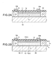
- Figure 2A is a sectional view of an Si-based PIN photo diode according to the present embodiment.
- a p - -type silicon semiconductor layer 11 having an impurity concentration of about 5 ⁇ 10 13 /cm 3 is formed on a p + -type silicon semiconductor substrate 10 having an impurity concentration of about 1 ⁇ 10 17 to 1 ⁇ 10 19 /cm 3 and, further, an n-type semiconductor layer 12 of about 10 15 /cm 3 is formed at the surface region of the p - -type semiconductor layer 11, whereby a pn-junction is formed.
- a p + -type semiconductor layer 13 is formed surrounding the PIN diode region. This becomes a take-out portion of a p-region and isolates the PIN diode region from other elements.
- a protective insulating film 14 comprised of silicon oxide etc. is formed at an upper layer of the n-type semiconductor layer 12 and p + -type semiconductor layer 13, contacts reaching respectively the n-type semiconductor layer 12 and the p + -type semiconductor layer 13 are opened, and take-out electrodes (15a and 15b) comprised of polycrystalline silicon or other metals etc. are formed.
- the depletion layer V spreads to the directions of the p - -type semiconductor layer 11 and n-type semiconductor layer from the pn-junction surface as shown in Fig. 2B.
- the depletion layer V spreads so that the total number of carriers becomes equal at the n-side and p-side, so spreads more to the p - -type semiconductor layer 11 side having a low carrier concentration.
- a depth and width of the depletion layer V spreading when the above predetermined inverse bias is applied are designed so that the numbers of carriers generated by photoelectric conversion become equal for example for light of wavelengths of two different regions, that is, a wavelength region of 780 nm used for a CD system and a wavelength region of 650 nm used for a DVD system.
- substantially the same extent of sensitivity and a high light receiving sensitivity is realized for a plurality of light having different wavelengths.
- a method of design so that the numbers of carriers generated by photoelectric conversion become equal for a plurality of light having different wavelengths will be explained below taking as an example a case of the 780 nm wavelength range and 650 nm wavelength range.
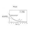
- Figure 3 shows the dependence on depth of a light intensity (relative value) of single wavelength light of 650 nm (A: solid line) and 780 nm (B: dotted line) entering the silicon.
- P i0 is a light intensity at the silicon surface and becomes a value a by light having a wavelength of 650 nm and a value b by light having a wavelength of 780 nm.
- ⁇ is an absorption coefficient (specifically, it becomes 2.7 ⁇ 10 3 /cm by light having a wavelength of 650 nm and 1.2 ⁇ 10 3 /cm by light having a wavelength of 780 nm).
- e indicates an elementary electric charge
- ⁇ a wavelength
- h Planck's constant a wavelength
- c the speed of light
- the numbers of carriers generated by photoelectric conversion of the light having wavelengths of 650 nm and 780 nm, that is, sensitivity to the 650 nm light and sensitivity to the 780 nm light, can be made substantially the same.
- an area of a region surrounded by an x-axis, a dotted line extending vertically from x 2 to the x-axis, and a light intensity curve (A, B) in Fig. 3 is the light receiving sensitivity between the depth x 1 to x 2 at the respective wavelengths.
- the sensitivities to the 650 nm light and the 780 nm light can be made substantially the same.
- the sensitivities to the 650 nm light and the 780 nm light can be made substantially the same in the same way.
- the light entering regions other than the above depletion layer also contributes to the sensitivity of the photo diode, but when the photoelectric conversion rate of the light entering the depletion layer is the highest and conversely light enters regions of high impurity concentration other than the depletion layer, the possibility of recombination immediately after the conversion to carriers (separation of electrons and holes) becomes high and the photoelectric conversion rate becomes low.
- the light enters regions of a low impurity concentration (I region, such as, p - region or n - region) other than the depletion layer, although the possibility of recombination immediately after the conversion to carriers (separation to electrons and holes) is not high, the resistance to the carrier becomes high due to the low impurity concentration, so the frequency characteristics of the photo diode become poor and a higher speed cannot be obtained.
- I region such as, p - region or n - region
- a substrate with a surface concentration of the p-type impurity of at least 1 ⁇ 10 17 /cm 3 it is preferable to use as a semiconductor substrate 10 a substrate with a surface concentration of the p-type impurity of at least 1 ⁇ 10 17 /cm 3 and to bring an end face S a of the depletion layer V on the semiconductor substrate 10 side and the surface S b of the semiconductor substrate 10 closer to a predetermined distance or less (for example, 3 ⁇ m or less).
- a predetermined distance or less for example, 3 ⁇ m or less
- the above can be also applied to both the cases where the region of a low impurity concentration (I region) is a p - -region or n - -region.
- the depth and width of the depletion layer V at the time that a predetermined inverse bias is applied are controlled so that the numbers of carriers generated by photoelectric conversion become the same for two types of light having different wavelengths, for example, a region of 780 nm wavelength used in a CD system and a region of 650 nm wavelength used in a DVD system, so the diode has substantially the same sensitivity for a plurality of light having different wavelengths of the 780 nm region and 650 nm region.
- a p - (I)-type silicon semiconductor layer 11 containing a p-type impurity of a low concentration of about 5 ⁇ 10 13 /cm 3 was formed by normal epitaxial growth on a p + -type silicon semiconductor substrate 10 having a p-type impurity concentration of 1 ⁇ 10 18 /cm 3 and an n-type semiconductor layer 12 containing an n-type impurity of about 5 ⁇ 10 15 /cm 3 was formed on the p-type semiconductor layer 11, whereby a PIN photo diode having a pn-junction was formed.
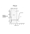
- a pn-junction is formed at a region c of the depth of about 1.5 ⁇ m from the surface.
- a point d where the p-type impurity concentration starts to rise from the p - (I)-type layer is formed at a depth of about 8 to 9 ⁇ m from the surface.
- a depletion layer V spreads in a region including a region of the depth of about 2 to 7 ⁇ m as shown in Fig. 4.
- the distance from an end face of the depletion layer V on the substrate side to a point where the p-type impurity concentration start to rise can be set to be 3 ⁇ m or less.
- Fig. 5 The results of measurement of the dependence on the wavelength of the incident light of the light receiving sensitivity of the PIN photo diode formed as explained above are shown in Fig. 5.
- a curve e in the figure indicates the dependence on the wavelength of the incident light of the light receiving sensitivity.
- a solid line f indicating an ideal dependence on the wavelength of the incident light of light receiving sensitivity in the case where the quantum efficiency is 100% is also shown.
- the light receiving sensitivities of the PIN photo diode formed as explained above in the cases of 650 nm and 780 nm are both about 0.42 A/W, that is, about the same sensitivity.
- a semiconductor device comprising a photo diode according to the above present embodiment can be preferably used as a light receiving element in an optical disk drive installed a dual CD/DVD system in.
- the present invention is not limited to the above example.
- the p-type impurity and the n-type impurity can be switched in the above example, that is, the invention can be applied to a PIN photo diode having a p-type semiconductor region at a surface layer portion of an n - -type semiconductor region.
- the wavelengths for which the sensitivities are designed to be the same are not limited to 650 nm and 780 nm. It is also possible to design the sensitivities to be the same for one of 650 nm or 780 nm and wavelength used in optical disk drives other than CD or DVD systems.
- the invention is not limited to a PIN photo diode and may be applied to photo diodes in general.
- the semiconductor device of the present invention has a photo diode designed so that a depletion layer spreads to a predetermined region so that the sensitivity of the photo diode to light of a first wavelength (for example, 780 nm) and sensitivity to light of a second wavelength (for example 650 nm) which is different from the first wavelength become substantially the same and therefore has substantially the same sensitivity to a plurality of light having different wavelengths.
- a first wavelength for example, 780 nm
- a second wavelength for example 650 nm
Landscapes
- Light Receiving Elements (AREA)
Abstract
Description

Claims (9)
- A semiconductor device having a photo diode comprising a first conductivity type semiconductor layer and a second conductivity type semiconductor layer formed at a surface layer portion of said first conductivity type semiconductor layer, wherein:
the sensitivity of said photo diode to light of a first wavelength and the sensitivity to light of a second wavelength which is different from said first wavelength are made to become substantially the same by designing a region in which a depletion layer spreads from a junction surface of said first conductivity type semiconductor layer and said second conductivity type semiconductor layer when inverse biases are applied to said first conductivity type semiconductor layer and said second conductivity type semiconductor layer. - A semiconductor device as set forth in claim 1, wherein:
the sensitivity of said photo diode to light of a first wavelength and the sensitivity to light of a second wavelength are made to become substantially the same by designing impurity concentrations and said inverse biases of said first conductivity type semiconductor layer and said second conductivity type semiconductor layer and by designing said region in which a depletion layer spreads. - A semiconductor device as set forth in claim 1, wherein said depletion layer is designed to spread in a region including a region 3 to 6 µm in the depth direction from a surface of said second conductivity type semiconductor layer.
- A semiconductor device as set forth in claim 1, wherein said depletion layer is designed to spread in a region including a region 2 to 7 µm in the depth direction from a surface of said second conductivity type semiconductor layer.
- A semiconductor device as set forth in claim 1, wherein said first conductivity type semiconductor layer is formed on a first conductivity type semiconductor substrate containing a first conductivity type impurity at a higher concentration than said first conductivity type semiconductor layer.
- A semiconductor device as set forth in claim 5, wherein a surface concentration of the first conductivity type impurity of said first conductivity type semiconductor substrate is at least 1×10¹⁷/cm3.
- A semiconductor device as set forth in claim 5, wherein a distance between an end face of said depletion layer at the first conductivity type semiconductor substrate side and the surface of said first conductivity type semiconductor substrate is 3 µm or less.
- A semiconductor device as set forth in claim 1, whereinsaid first wavelength is 780 nm andsaid second wavelength is 650 nm.
- A semiconductor device comprising a first conductivity type semiconductor substrate, a first conductivity type semiconductor layer formed on a first conductivity type semiconductor substrate and containing a first conductivity type impurity at a lower concentration than said first conductivity type semiconductor substrate, and a second conductivity type semiconductor layer formed at a surface layer portion of said first conductivity type semiconductor layer, wherein:a photo diode is formed by spreading a depletion layer from a junction surface of said first conductivity type semiconductor layer and said second conductivity type semiconductor layer when inverse biases are applied to said first conductivity type semiconductor layer and said second conductivity type semiconductor layer, andthe concentrations of the impurity of said first and second conductivity layers are adjusted so that the depletion layer spreading region is made wherein the sensitivity of said photo diode to light of a first wavelength and the sensitivity to light of a second wavelength which is different from said first wavelength become substantially the same.
Applications Claiming Priority (2)
| Application Number | Priority Date | Filing Date | Title |
|---|---|---|---|
| JP2000209780 | 2000-07-11 | ||
| JP2000209780A JP2002026366A (en) | 2000-07-11 | 2000-07-11 | Semiconductor device |
Publications (3)
| Publication Number | Publication Date |
|---|---|
| EP1172865A2 true EP1172865A2 (en) | 2002-01-16 |
| EP1172865A3 EP1172865A3 (en) | 2003-08-13 |
| EP1172865B1 EP1172865B1 (en) | 2014-12-03 |
Family
ID=18706138
Family Applications (1)
| Application Number | Title | Priority Date | Filing Date |
|---|---|---|---|
| EP01116841.6A Expired - Lifetime EP1172865B1 (en) | 2000-07-11 | 2001-07-10 | Semiconductor photosensitive device |
Country Status (4)
| Country | Link |
|---|---|
| US (1) | US6798001B2 (en) |
| EP (1) | EP1172865B1 (en) |
| JP (1) | JP2002026366A (en) |
| KR (2) | KR20020005990A (en) |
Families Citing this family (11)
| Publication number | Priority date | Publication date | Assignee | Title |
|---|---|---|---|---|
| JP4539011B2 (en) * | 2002-02-20 | 2010-09-08 | 富士電機システムズ株式会社 | Semiconductor device |
| US7078260B2 (en) * | 2003-12-31 | 2006-07-18 | Dongbu Electronics Co., Ltd. | CMOS image sensors and methods for fabricating the same |
| KR100595898B1 (en) * | 2003-12-31 | 2006-07-03 | 동부일렉트로닉스 주식회사 | Image sensor and its manufacturing method |
| JP4354931B2 (en) * | 2005-05-19 | 2009-10-28 | パナソニック株式会社 | Solid-state imaging device and manufacturing method thereof |
| US7638852B2 (en) | 2006-05-09 | 2009-12-29 | Taiwan Semiconductor Manufacturing Company, Ltd. | Method of making wafer structure for backside illuminated color image sensor |
| US8704277B2 (en) | 2006-05-09 | 2014-04-22 | Taiwan Semiconductor Manufacturing Company, Ltd. | Spectrally efficient photodiode for backside illuminated sensor |
| US7791170B2 (en) | 2006-07-10 | 2010-09-07 | Taiwan Semiconductor Manufacturing Company, Ltd. | Method of making a deep junction for electrical crosstalk reduction of an image sensor |
| US8436443B2 (en) | 2006-09-29 | 2013-05-07 | Taiwan Semiconductor Manufacturing Company, Ltd. | Backside depletion for backside illuminated image sensors |
| US7999342B2 (en) | 2007-09-24 | 2011-08-16 | Taiwan Semiconductor Manufacturing Company, Ltd | Image sensor element for backside-illuminated sensor |
| JP2010278045A (en) * | 2009-05-26 | 2010-12-09 | Panasonic Corp | Optical semiconductor device |
| JP7040140B2 (en) * | 2018-03-07 | 2022-03-23 | セイコーエプソン株式会社 | Photoelectric conversion elements, photoelectric conversion modules and electronic devices |
Family Cites Families (10)
| Publication number | Priority date | Publication date | Assignee | Title |
|---|---|---|---|---|
| JPS4917189A (en) * | 1972-06-02 | 1974-02-15 | ||
| US4127932A (en) * | 1976-08-06 | 1978-12-05 | Bell Telephone Laboratories, Incorporated | Method of fabricating silicon photodiodes |
| JPS594183A (en) * | 1982-06-30 | 1984-01-10 | Fujitsu Ltd | Color detecting system |
| US4749851A (en) * | 1986-08-29 | 1988-06-07 | Technische Universiteit Delft | Method and circuit for determining the wave-length of light |
| JP2662062B2 (en) * | 1989-12-15 | 1997-10-08 | キヤノン株式会社 | Photoelectric conversion device |
| CA2108748A1 (en) | 1992-10-23 | 1994-04-24 | Robert M. Griffin | Self-supporting/self-centering filament |
| DE19613820A1 (en) * | 1996-04-09 | 1997-10-23 | Forschungszentrum Juelich Gmbh | Structure with a pin or nip layer sequence |
| JPH10190037A (en) * | 1996-12-20 | 1998-07-21 | Stanley Electric Co Ltd | PIN photodiode |
| US5886374A (en) * | 1998-01-05 | 1999-03-23 | Motorola, Inc. | Optically sensitive device and method |
| JP4131031B2 (en) * | 1998-03-17 | 2008-08-13 | ソニー株式会社 | Semiconductor device having light receiving element, optical pickup device, and method of manufacturing semiconductor device having light receiving element |
-
2000
- 2000-07-11 JP JP2000209780A patent/JP2002026366A/en active Pending
-
2001
- 2001-07-10 EP EP01116841.6A patent/EP1172865B1/en not_active Expired - Lifetime
- 2001-07-10 US US09/902,177 patent/US6798001B2/en not_active Expired - Fee Related
- 2001-07-10 KR KR1020010041134A patent/KR20020005990A/en not_active Ceased
-
2008
- 2008-04-22 KR KR1020080036977A patent/KR20080064761A/en not_active Ceased
Non-Patent Citations (1)
| Title |
|---|
| None |
Also Published As
| Publication number | Publication date |
|---|---|
| EP1172865B1 (en) | 2014-12-03 |
| JP2002026366A (en) | 2002-01-25 |
| EP1172865A3 (en) | 2003-08-13 |
| KR20080064761A (en) | 2008-07-09 |
| KR20020005990A (en) | 2002-01-18 |
| US20020017655A1 (en) | 2002-02-14 |
| US6798001B2 (en) | 2004-09-28 |
Similar Documents
| Publication | Publication Date | Title |
|---|---|---|
| CA2050362C (en) | Photo-sensing device | |
| JP4220688B2 (en) | Avalanche photodiode | |
| US3959646A (en) | Avalanche photo-diodes | |
| CA1132693A (en) | Demultiplexing photodetector | |
| KR20080064761A (en) | Semiconductor devices | |
| EP0142316A2 (en) | Improved p-i-n- and avalanche photodiodes | |
| KR950003950B1 (en) | Photo-sensing device | |
| US7696593B2 (en) | PIN-type photo detecting element with three semiconductor layers, and window semiconductor layer having controlled thickness | |
| US20070158664A1 (en) | Mesa structure photon detection circuit | |
| US4323911A (en) | Demultiplexing photodetectors | |
| JP4861388B2 (en) | Avalanche photodiode | |
| EP0308335B1 (en) | Ingaas/inp type pin photodiodes | |
| EP0522746B1 (en) | Semiconductor photodetector device | |
| US5115295A (en) | Photodetector device | |
| CA2232084C (en) | Semiconductor heterostructure radiation detector having two spectral sensitivity ranges | |
| US7619240B2 (en) | Semiconductor photodetector, device for multispectrum detection of electromagnetic radiation using such a photodetector and method for using such a device | |
| JPH07105522B2 (en) | Semiconductor device | |
| KR100424366B1 (en) | A Photodiode With A Diffusion-Layer Of Dispersion-Distribution Pattern And Fabrication Method Thereof And A Substrate And An Electronic Machine Thereby | |
| JP2848345B2 (en) | Infrared detector | |
| Kim et al. | Crosstalk measurements on a linear array of deep U-groove isolated silicon photodiodes | |
| KR100463425B1 (en) | A structure of Photo Diode cells in a PDIC for a optical pickup, and its manufacturing method | |
| JPH0548137A (en) | Semiconductor light receiving element | |
| Zheng et al. | A 12× 12 InGaAs/InAlAs Avalanche Photodetector Array | |
| JPS6229917B2 (en) |
Legal Events
| Date | Code | Title | Description |
|---|---|---|---|
| PUAI | Public reference made under article 153(3) epc to a published international application that has entered the european phase |
Free format text: ORIGINAL CODE: 0009012 |
|
| AK | Designated contracting states |
Kind code of ref document: A2 Designated state(s): AT BE CH CY DE DK ES FI FR GB GR IE IT LI LU MC NL PT SE TR |
|
| AX | Request for extension of the european patent |
Free format text: AL;LT;LV;MK;RO;SI |
|
| PUAL | Search report despatched |
Free format text: ORIGINAL CODE: 0009013 |
|
| AK | Designated contracting states |
Designated state(s): AT BE CH CY DE DK ES FI FR GB GR IE IT LI LU MC NL PT SE TR |
|
| AX | Request for extension of the european patent |
Extension state: AL LT LV MK RO SI |
|
| RIC1 | Information provided on ipc code assigned before grant |
Ipc: 7H 01L 31/101 B Ipc: 7H 01L 31/105 B Ipc: 7H 01L 31/11 A |
|
| 17P | Request for examination filed |
Effective date: 20040113 |
|
| AKX | Designation fees paid |
Designated state(s): DE FR GB |
|
| 17Q | First examination report despatched |
Effective date: 20070507 |
|
| GRAP | Despatch of communication of intention to grant a patent |
Free format text: ORIGINAL CODE: EPIDOSNIGR1 |
|
| INTG | Intention to grant announced |
Effective date: 20140623 |
|
| GRAS | Grant fee paid |
Free format text: ORIGINAL CODE: EPIDOSNIGR3 |
|
| GRAA | (expected) grant |
Free format text: ORIGINAL CODE: 0009210 |
|
| RIN1 | Information on inventor provided before grant (corrected) |
Inventor name: ARAI, CHIHIRO, SONY CORPORATION Inventor name: FUJISAWA, TOMOTAKA, SONY CORPORATION |
|
| AK | Designated contracting states |
Kind code of ref document: B1 Designated state(s): DE FR GB |
|
| RAP1 | Party data changed (applicant data changed or rights of an application transferred) |
Owner name: SONY CORPORATION |
|
| REG | Reference to a national code |
Ref country code: GB Ref legal event code: FG4D |
|
| REG | Reference to a national code |
Ref country code: DE Ref legal event code: R096 Ref document number: 60149142 Country of ref document: DE Effective date: 20150115 |
|
| REG | Reference to a national code |
Ref country code: DE Ref legal event code: R097 Ref document number: 60149142 Country of ref document: DE |
|
| PLBE | No opposition filed within time limit |
Free format text: ORIGINAL CODE: 0009261 |
|
| STAA | Information on the status of an ep patent application or granted ep patent |
Free format text: STATUS: NO OPPOSITION FILED WITHIN TIME LIMIT |
|
| 26N | No opposition filed |
Effective date: 20150904 |
|
| REG | Reference to a national code |
Ref country code: DE Ref legal event code: R119 Ref document number: 60149142 Country of ref document: DE |
|
| GBPC | Gb: european patent ceased through non-payment of renewal fee |
Effective date: 20150710 |
|
| PG25 | Lapsed in a contracting state [announced via postgrant information from national office to epo] |
Ref country code: GB Free format text: LAPSE BECAUSE OF NON-PAYMENT OF DUE FEES Effective date: 20150710 Ref country code: DE Free format text: LAPSE BECAUSE OF NON-PAYMENT OF DUE FEES Effective date: 20160202 |
|
| REG | Reference to a national code |
Ref country code: FR Ref legal event code: ST Effective date: 20160331 |
|
| PG25 | Lapsed in a contracting state [announced via postgrant information from national office to epo] |
Ref country code: FR Free format text: LAPSE BECAUSE OF NON-PAYMENT OF DUE FEES Effective date: 20150731 |