EP1172849A2 - Verfahren zur Erzeugung einer Mehrzahl von Chips mit Halbleiterbauelementen, die eine Schicht mit definierter elektrischer Polarisation aufweisen - Google Patents
Verfahren zur Erzeugung einer Mehrzahl von Chips mit Halbleiterbauelementen, die eine Schicht mit definierter elektrischer Polarisation aufweisen Download PDFInfo
- Publication number
- EP1172849A2 EP1172849A2 EP01117039A EP01117039A EP1172849A2 EP 1172849 A2 EP1172849 A2 EP 1172849A2 EP 01117039 A EP01117039 A EP 01117039A EP 01117039 A EP01117039 A EP 01117039A EP 1172849 A2 EP1172849 A2 EP 1172849A2
- Authority
- EP
- European Patent Office
- Prior art keywords
- conductor tracks
- temporary
- semiconductor components
- chips
- metallization
- Prior art date
- Legal status (The legal status is an assumption and is not a legal conclusion. Google has not performed a legal analysis and makes no representation as to the accuracy of the status listed.)
- Granted
Links
Images



Classifications
-
- H—ELECTRICITY
- H10—SEMICONDUCTOR DEVICES; ELECTRIC SOLID-STATE DEVICES NOT OTHERWISE PROVIDED FOR
- H10P—GENERIC PROCESSES OR APPARATUS FOR THE MANUFACTURE OR TREATMENT OF DEVICES COVERED BY CLASS H10
- H10P52/00—Grinding, lapping or polishing of wafers, substrates or parts of devices
-
- H—ELECTRICITY
- H03—ELECTRONIC CIRCUITRY
- H03H—IMPEDANCE NETWORKS, e.g. RESONANT CIRCUITS; RESONATORS
- H03H3/00—Apparatus or processes specially adapted for the manufacture of impedance networks, resonating circuits, resonators
- H03H3/007—Apparatus or processes specially adapted for the manufacture of impedance networks, resonating circuits, resonators for the manufacture of electromechanical resonators or networks
- H03H3/02—Apparatus or processes specially adapted for the manufacture of impedance networks, resonating circuits, resonators for the manufacture of electromechanical resonators or networks for the manufacture of piezoelectric or electrostrictive resonators or networks
-
- H—ELECTRICITY
- H10—SEMICONDUCTOR DEVICES; ELECTRIC SOLID-STATE DEVICES NOT OTHERWISE PROVIDED FOR
- H10N—ELECTRIC SOLID-STATE DEVICES NOT OTHERWISE PROVIDED FOR
- H10N15/00—Thermoelectric devices without a junction of dissimilar materials; Thermomagnetic devices, e.g. using the Nernst-Ettingshausen effect
- H10N15/10—Thermoelectric devices using thermal change of the dielectric constant, e.g. working above and below the Curie point
-
- H—ELECTRICITY
- H10—SEMICONDUCTOR DEVICES; ELECTRIC SOLID-STATE DEVICES NOT OTHERWISE PROVIDED FOR
- H10N—ELECTRIC SOLID-STATE DEVICES NOT OTHERWISE PROVIDED FOR
- H10N30/00—Piezoelectric or electrostrictive devices
- H10N30/01—Manufacture or treatment
- H10N30/07—Forming of piezoelectric or electrostrictive parts or bodies on an electrical element or another base
- H10N30/071—Mounting of piezoelectric or electrostrictive parts together with semiconductor elements, or other circuit elements, on a common substrate
-
- H—ELECTRICITY
- H10—SEMICONDUCTOR DEVICES; ELECTRIC SOLID-STATE DEVICES NOT OTHERWISE PROVIDED FOR
- H10P—GENERIC PROCESSES OR APPARATUS FOR THE MANUFACTURE OR TREATMENT OF DEVICES COVERED BY CLASS H10
- H10P54/00—Cutting or separating of wafers, substrates or parts of devices
Definitions
- each a first semiconductor component that has a layer with a defined electrical polarization exhibit.
- the invention relates to a method for generating analog to one another built-up chips, each a first semiconductor component, the one layer with a defined electrical Has polarization.
- Such a first semiconductor device can, for. B. mechanical or thermal radiation into electrical voltage changes convert or vice versa.
- the layer of first semiconductor device which is usually between two Electrodes is arranged from a piezoelectric or pyroelectric material.
- the layer After depositing the material to create the layer however, the layer is less in a state electrical polarization.
- a polarization process is required. This will a high electrical at a temperature of over 150 ° C Field applied in the layer, which is due to the so-called ferroelectric effect to permanent polarization of the material of the layer. This can be done through generation of a voltage drop in the layer by the Suitable voltages are applied to electrodes.
- Each chip only includes a first one described above Semiconductor component, so can be a method of manufacture of several chips constructed analogously to one another by means of of a wafer can be easily realized as all first semiconductor components the chips on the wafer to polarize their layers can be connected in parallel.
- each chip next to the first semiconductor device also has at least one second semiconductor component, that are connected to the first semiconductor component should.
- a parallel connection of the first Semiconductor components with the desired interconnection of the Semiconductor components may be incompatible with each other.
- the invention is therefore based on the object of a method for the generation of chips constructed analogously to one another in each case a first semiconductor component that has a layer has a defined electrical polarization, and a have second semiconductor component, using a To provide wafers that are effective and inexpensive.
- each at least a first semiconductor component that has a layer with a has defined electrical polarization in which the chips are produced on a wafer, whereby per the first semiconductor component, the layer that is not initially has its full polarization.
- Per chip generates at least one second semiconductor component.
- temporary conductor tracks conductive material is deposited and structured so that each layer of the first Semiconductor components between two of the temporary conductor tracks is switched, and that each temporary conductor track with sub-pages or tops of the layers of the first semiconductor components several chips is connected to the wafer.
- the layers of the first semiconductor components are poled, by applying voltages to the temporary traces. After polarization of the layers of the first semiconductor components the temporary conductor tracks at least in sections away.
- the tensions to poling the layers are due to the temporary conductor tracks in only a few manageable places placed on the wafer so that the process is efficient and is inexpensive.
- the first semiconductor component can be produced in such a way that it electrical or thermal radiation into electrical voltage changes converts or vice versa.
- the Layer of the first semiconductor component made of a piezo or pyroelectric material.
- the layer of the first Semiconductor component can for example be made of PZT (lead zirconium titanate) be generated.
- the first semiconductor component is a bulk acoustic wave Resonator, a surface acoustic wave resonator.
- a lower electrode, above the layer and above an upper electrode become.
- Conductive can be used to generate the temporary interconnects Material is deposited and structured in such a way that any temporary trace with bottom or top electrodes of the first semiconductor components of a plurality of chips is.
- the top and bottom Electrodes of the first semiconductor components at the same time as Electrodes for polishing the layers of the first semiconductor components used.
- a temporary upper electrode at the same time or before the temporary one Traces are generated.
- After polarization of the layers of the first semiconductor components can temporary top electrodes are removed, and then new upper electrodes are generated.
- the process is based on the first semiconductor components and the second semiconductor components, an insulating intermediate layer deposited. Then contact holes are made in the intermediate layer to the first and the second semiconductor components generated. At least for the lower ones and for the upper electrodes of the first semiconductor components Contact holes created. It becomes a diffusion barrier layer deposited from conductive material with such a thickness, that it does not fill the contact holes. For generation of contacts becomes conductive material of one Thickness deposited over the diffusion barrier layer it fills the contact holes. This conductive material will etched back so far that the diffusion barrier layer partially is exposed. By structuring the diffusion barrier layer the temporary tracks are created. The temporary conductor tracks therefore consist of parts of the diffusion barrier layer. After polarizing the layers of the first semiconductor components is used to generate the conductor tracks deposited the metallization conductive material and structured, being outside the conductor tracks of the metallization removed parts of the diffusion barrier layer become.
- the diffusion barrier layer which is usually intended for contacts at the same time used for the generation of the temporary interconnects.
- the removal of the metallization outside the traces lying parts of the diffusion barrier layer preferably by overetching the conductive material at the Generation of the conductor tracks of the metallization.
- the temporary Conductor tracks are used when structuring the conductive material to generate the conductor tracks of the metallization in sections away. For section-by-section removal the temporary conductor tracks is therefore not an additional mask or additional etching step required.
- the intermediate layer consists, for example, of SiO 2 .
- the diffusion barrier layer consists for example of titanium, titanium nitride or a combination of the two materials.
- the diffusion barrier layer is preferably between 20 and 50 nm thick.
- the conductive material for producing the contacts contains, for example, tungsten.
- the conductive material for producing the conductor tracks of the metallization contains, for example, AlSiCu.
- the temporary interconnects can after polarization of the layers of the first semiconductor components completely through unmasked selective etching be removed. So the temporary traces before depositing the conductive material to produce the conductor tracks the metallization removed. Because the temporary traces to be removed completely is not an additional one Mask required for removal.
- the temporary conductor tracks are generated by sputtering amorphous silicon.
- CF 4 can be used as the etching agent in order to completely remove the temporary conductor tracks by unmasked selective dry etching.
- Such an etchant can be used to selectively etch to SiO 2 .
- the temporary conductor tracks after polarization of the layers in sections removed that remaining parts of the temporary Conductors first parts of the metallization conductors form.
- To create two parts of the conductor tracks of the metallization conductive material is deposited and structured.
- the temporary traces and the Metallization interconnects made of the same conductive material generated.
- the metallization becomes the conductive material structured that the first parts of the conductor tracks of the metallization under parts of the second parts of the conductor tracks the metallization.
- a temporary mask is used for the temporary conductor tracks, the locations where the metallization traces should be generated, covered.
- a second mask is used, covering the same spots as the first Mask.
- the conductor tracks of the metallization are in areas where there are also parts of the temporary conductor tracks were produced, particularly thick and consequently have one there especially small electrical resistance.
- the temporary traces and the traces metallization from various conductive materials generated.
- the second can be generated Parts of the conductor tracks of the metallization the corresponding conductive material are structured so that the first parts of the conductor tracks of the metallization next to the second parts of the conductor tracks of the metallization.
- a mask is used that covers all areas in which the conductor tracks of the metallization are to be created except for areas in which the first parts of the conductor tracks of the metallization were covered, and it the material of the second parts selectively becomes the material of the first parts of the conductor tracks of the metallization etched.
- the second semiconductor components can, for example, transistors or capacitors.
- the second semiconductor components are similar to built the first semiconductor devices. This is done for the second semiconductor components each have a layer with a defined electrical polarization generated.
- the temporary Conductor tracks are created so that each layer of the second Semiconductor components between two of the temporary conductor tracks is switched, and that each temporary conductor track with sub-pages or tops of the layers of the second semiconductor components several of the chips are connected. Any temporary Conductor contacts both first and second Semiconductor devices.
- a temporary trace can e.g. B. Undersides of first and undersides of second semiconductor components, or sub-pages of first and top pages of second semiconductor components, or tops of first and undersides of second semiconductor components, or Top sides of first and top sides of second semiconductor components to contact.
- the other semiconductor components can for example transistors or capacitors or be constructed similarly to the first semiconductor components.
- the chip can be manufactured, for example, so that it includes a bulk acoustic wave filter.
- the application of the voltages to the temporary conductor tracks preferably takes place at elevated temperature, e.g. at over 150 ° C instead.
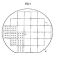
- the starting material a wafer W made of silicon is used. Be on the wafer W. Chips C generated. Each nine chips C are to a field F grouped. The fields F are in rows and columns on the Wafer W arranged (see Figure 1). The chips C are analog built up to each other. For the sake of simplicity, FIG not all chips C shown.
- each chip C six are constructed analogously to one another Semiconductor components generated. The manufacturing process will explained using a first semiconductor component.
- An approximately 500 nm thick insulating layer I made of SiO 2 is produced on the wafer W (see FIG. 2). Platinum is deposited in a thickness of approx. 100 nm and structured to form a lower electrode U.
- PZT is applied in a thickness of approx. 1500 nm and above platinum deposited in a thickness of about 100 nm.
- the platinum and the PZT are structured by etching, around a piezoelectric layer S and one above to form upper electrode O.
- the first semiconductor device comprises the lower electrode U, the layer S and the upper one Electrode O. At this point, layer S has a small one electrical polarization. The same applies for the remaining five semiconductor components of the chip C. Die Semiconductor components are called bulk acoustic wave resonators designed.
- SiO 2 is deposited in a thickness of approximately 1 ⁇ m and planarized. Through masked etching, contact holes are opened, which extend up to the upper electrodes O and the lower electrodes U.
- an approximately 30 nm thick partial layer made of titanium and an approximately 30 nm thick partial layer made of TiN is produced above it.
- the two sub-layers together form a diffusion barrier layer D (see Figure 3).
- the diffusion barrier layer D is so thin that it does not fill the contact holes.
- tungsten is used in a thickness of Approx. 800 nm deposited and etched back until parts of the diffusion barrier layer D are exposed (see Figure 3).
- the diffusion barrier layer D structured into temporary conductor tracks TL.
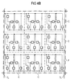
- the temporary conductor tracks TL branch out into the fields F towards the individual chips C. (see Figures 4a and 4b).
- the temporary conductor tracks TL are with upper electrodes O or with lower electrodes U of the semiconductor components connected. Any semiconductor device is connected between two of the temporary conductor tracks TL.
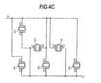
- FIG. 4c shows the circuit diagram of a chip C. its six semiconductor devices that are associated with the temporary Conductor tracks TL are connected.
- the layers S of the semiconductor components are attached to the two temporary traces TL of each column of fields F by means of a voltage source Q voltages and thereby creates a voltage drop in the layers S.
- the two temporary interconnects are TL the third column of the fields connected to the voltage source Q, so that the layers S of the chips C of the third column of the fields F are polarized.
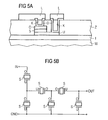
- AlSiCu is in one Deposition of approx. 1 ⁇ m and masked by masked etching Structured conductor tracks L of a metallization of the chips C. (see Figures 5a and 5b). When structuring, too Titan and TiN removed, so that the temporary conductor tracks TL removed in sections.
- the semiconductor components become through the conductor tracks L of the metallization the chips C wired so that everyone Chip C forms a bulk acoustic wave filter (see figure 5b).
- the Wafer W is sawn so that the chips C are separated from one another become.
- a second embodiment the same as in the first Exemplary embodiment produces a wafer with chips in fields, each chip having six semiconductor devices.
- an insulating Layer I ', a lower electrode U', a layer S ', a upper electrode O ', an intermediate layer Z', a diffusion barrier layer D 'and contacts K' generated (see Figure 6a).
- AlSiCu in is used to generate temporary conductor tracks TL ' deposited with a thickness of approx. 800 nm and with the help of a Textured paint mask.
- the temporary traces TL ' run exactly as in the first embodiment.
- each chip comprises six Semiconductor devices. Until the contacts are made, that is Manufacturing process identical to the manufacturing process of the first embodiment.
- Amorphous silicon is used to create temporary interconnects deposited in a thickness of approx. 50 nm and together structured with the diffusion barrier layer.
- the history the temporary conductor tracks correspond to the course of the temporary ones Conductor tracks TL of the first embodiment.
- the temporary conductor tracks are completely by dry etching with z. B. CF 4 removed.
- AlSiCu is deposited in a thickness of approx. 800 nm and structured using a mask made of photoresist.
- the conductor tracks the metallization run like the conductor tracks L the metallization of the first embodiment.
Landscapes
- Engineering & Computer Science (AREA)
- Manufacturing & Machinery (AREA)
- Internal Circuitry In Semiconductor Integrated Circuit Devices (AREA)
- Metal-Oxide And Bipolar Metal-Oxide Semiconductor Integrated Circuits (AREA)
Abstract
Description
- Figur 1
- zeigt eine Aufsicht auf einen Wafer mit zu Feldern gruppierten Chips.
- Figur 2
- zeigt einen Ausschnitt eines Querschnitts durch den Wafer mit einem ersten Halbleiterbauelement eines Chips, nachdem eine isolierende Schicht, eine untere Elektrode, eine Schicht, eine obere Elektrode und eine Zwischenschicht erzeugt wurden.
- Figur 3
- zeigt den Ausschnitt aus Figur 2, nachdem eine Diffusionsbarrierenschicht und Kontakte erzeugt wurden.
- Figur 4a
- zeigt die Aufsicht auf den Wafer aus Figur 1, nachdem temporäre Leiterbahnen erzeugt wurden und eine Spannungsquelle angeschlossen wurde.
- Figur 4b
- zeigt einen Ausschnitt der Aufsicht aus Figur 4a mit den Chips eines Feldes.
- Figur 4c
- zeigt das Schaltbild eines Chips mit den temporären Leiterbahnen.
- Figur 5a
- zeigt den Querschnitt aus Figur 3, nachdem die temporären Leiterbahnen abschnittsweise entfernt wurden und Leiterbahnen einer Metallisierung erzeugt wurden.
- Figur 5b
- zeigt das Schaltbild eines Chips mit den Leiterbahnen der Metallisierung.
- Figur 6a
- zeigt einen Ausschnitt eines Querschnitts durch einen zweiten Wafer mit einem ersten Halbleiterbauelement, nachdem eine isolierende Schicht, eine untere Elektrode, eine Schicht, eine obere Elektrode, eine Zwischenschicht, eine Diffusionsbarrierenschicht, Kontakte und temporäre Leiterbahnen erzeugt wurden.
- Figur 6b
- zeigt den Ausschnitt aus Figur 6a, nachdem die temporären Leiterbahnen abschnittsweise entfernt wurden und Leiterbahnen einer Metallisierung erzeugt wurden.
- c
- Chip
- D, D'
- Diffusionsbarrierenschicht
- F
- Feld
- I, I'
- isolierende Schicht
- K, K'
- Kontakt
- L, L'
- Leiterbahn einer Metallisierung
- O, O'
- Obere Elektrode
- S, S'
- Schicht
- TL, TL'
- temporäre Leiterbahn
- U, U'
- Untere Elektrode
- W
- Wafer
- Z, Z'
- Zwischenschicht
Claims (12)
- Verfahren zur Erzeugung analog zueinander aufgebauter Chips, die jeweils ein erstes Halbleiterbauelement, das eine Schicht mit einer definierten elektrischen Polarisation aufweist, aufweisen,bei dem die Chips (C) auf einem Wafer (W) erzeugt werden,die Schichten (S) der ersten Halbleiterbauelemente werden so erzeugt, daß sie zunächst nicht ihre volle Polarisation aufweisen,bei dem pro Chip (C) mindestens ein zweites Halbleiterbauelement erzeugt wird,bei dem zur Erzeugung temporärer Leiterbahnen (TL) leitendes Material abgeschieden und derart strukturiert wird, daß jede Schicht (S) der ersten Halbleiterbauelemente zwischen zwei der temporären Leiterbahnen (TL) geschaltet ist, und daß jede temporäre Leiterbahn (TL) mit Unterseiten oder Oberseiten der Schichten (S) der ersten Halbleiterbauelemente mehrerer der Chips (C) verbunden ist,bei dem die Schichten (S) der ersten Halbleiterbauelemente gepolt werden, indem Spannungen an die temporären Leiterbahnen (TL) angelegt werden,bei dem die temporären Leiterbahnen (TL) nach Polarisierung der Schichten (S) der ersten Halbleiterbauelemente zumindest abschnittsweise entfernt werden,bei dem zum Verschalten der ersten Halbleiterbauelemente mit den zweiten Halbleiterbauelementen Leiterbahnen (L) einer Metallisierung der Chips (C) erzeugt werden,bei dem die Chips (C) nach deren Fertigstellung vereinzelt werden.
- Verfahren nach Anspruch 1,bei dem die Schichten (S) der ersten Halbleiterbauelemente aus einem piezo- oder pyroelektrischen Material erzeugt werden.
- Verfahren nach Anspruch 2,bei dem das erste Halbleiterbauelement als Bulk-Acoustic-Wave-Resonator erzeugt wird.
- Verfahren nach einem der Ansprüche 1 bis 3,bei dem pro erstem Halbleiterbauelement eine untere Elektrode (U), darüber die Schicht (S), die zunächst nicht ihre volle Polarisation aufweist, und darüber eine obere Elektrode (O) erzeugt werden,bei dem zur Erzeugung der temporären Leiterbahnen (TL) leitendes Material abgeschieden und derart strukturiert wird, daß jede temporäre Leiterbahn mit (TL) unteren (U) oder oberen Elektroden (O) der ersten Halbleiterbauelemente mehrerer der Chips (C) verbunden ist.
- Verfahren nach Anspruch 4,bei dem über den ersten Halbleiterbauelementen und den zweiten Halbleiterbauelementen eine isolierende Zwischenschicht (Z) abgeschieden wird,bei dem Kontaktlöcher in der Zwischenschicht (Z) zu den ersten Halbleiterbauelementen und den zweiten Halbleiterbauelementen erzeugt werden,bei dem eine Diffusionsbarrierenschicht (D) aus leitendem Material mit einer solchen Dicke abgeschieden wird, daß sie die Kontaktlöcher nicht ausfüllt,bei dem zur Erzeugung von Kontakten (K) leitendes Material in einer solchen Dicke abgeschieden wird, daß die Kontaktlöcher ausgefüllt werden, und soweit rückgeätzt wird, daß die Diffusionsbarrierenschicht (D) freigelegt wird,bei dem durch Strukturierung der Diffusionsbarrierenschicht (D) die temporären Leiterbahnen (TL) erzeugt werden,bei dem nach Polarisierung der Schichten (S) der ersten Halbleiterbauelemente zur Erzeugung der Leiterbahnen (L) der Metallisierung leitendes Material abgeschieden und strukturiert wird, wobei außerhalb der Leiterbahnen (L) der Metallisierung liegende Teile der Diffusionsbarrierenschicht (D) entfernt werden.
- Verfahren nach einem der Ansprüche 1 bis 4,bei dem die temporären Leiterbahnen nach Polarisierung der Schichten der ersten Halbleiterbauelemente vollständig durch unmaskiertes selektives Ätzen entfernt werden.
- Verfahren nach Anspruch 6,bei dem die temporären Leiterbahnen aus amorphem Silizium erzeugt werden.
- Verfahren nach einem der Ansprüche 1 bis 4,bei dem die temporären Leiterbahnen (TL') nach Polarisierung der Schichten (S') abschnittsweise derart entfernt werden, daß übrigbleibende Teile der temporären Leiterbahnen (TL') erste Teile der Leiterbahnen (L') der Metallisierung bilden,bei dem zur Erzeugung zweiter Teile der Leiterbahnen (L') der Metallisierung leitendes Material abgeschieden und strukturiert wird.
- Verfahren nach Anspruch 8,bei dem die temporären Leiterbahnen (TL') und die Leiterbahnen (L') der Metallisierung aus demselben leitenden Material erzeugt werden,bei dem zur Erzeugung der zweiten Teile der Leiterbahnen (L') der Metallisierung das leitende Material derart strukturiert wird, daß die ersten Teile der Leiterbahnen (L') der Metallisierung unter Teilen der zweiten Teile der Leiterbahnen (L') der Metallisierung liegen.
- Verfahren nach einem der Ansprüche 1 bis 9,bei dem für die zweiten Halbleiterbauelemente jeweils eine Schicht (S) mit einer definierten elektrischen Polarisation erzeugt wird,bei dem die temporären Leiterbahnen (TL) so erzeugt werden, daß jede Schicht (S) der zweiten Halbleiterbauelemente zwischen zwei der temporären Leiterbahnen (TL) geschaltet ist, und daß jede temporäre Leiterbahn (TL) mit Unterseiten oder Oberseiten der Schichten (S) der zweiten Halbleiterbauelemente mehrerer der Chips (C) verbunden ist.
- Verfahren nach einem der Ansprüche 1 bis 10,bei dem die Chips (C) so erzeugt werden, daß sie in Felder (F), die in Reihen und Spalten auf dem Wafer (W) angeordnet sind, gruppiert sind,bei dem für jede Spalte der Felder (F) zwei der temporären Leiterbahnen (TL) erzeugt werden, die sich innerhalb der Felder zu den einzelnen Chips (C) hin verästeln.
- Verfahren nach einem der Ansprüche 1 bis 11,bei dem pro Chip (C) weitere Halbleiterbauelemente erzeugt werden.
Applications Claiming Priority (2)
| Application Number | Priority Date | Filing Date | Title |
|---|---|---|---|
| DE10034085A DE10034085C2 (de) | 2000-07-13 | 2000-07-13 | Verfahren zur Erzeugung analog zueinander aufgebauter Chips, die jeweils ein erstes Halbleiterbauelement, das eine Schicht mit einer definierten elektrischen Polarisation aufweist, aufweisen |
| DE10034085 | 2000-07-13 |
Publications (3)
| Publication Number | Publication Date |
|---|---|
| EP1172849A2 true EP1172849A2 (de) | 2002-01-16 |
| EP1172849A3 EP1172849A3 (de) | 2005-01-26 |
| EP1172849B1 EP1172849B1 (de) | 2006-04-26 |
Family
ID=7648811
Family Applications (1)
| Application Number | Title | Priority Date | Filing Date |
|---|---|---|---|
| EP01117039A Expired - Lifetime EP1172849B1 (de) | 2000-07-13 | 2001-07-12 | Verfahren zur Erzeugung einer Mehrzahl von Chips mit Halbleiterbauelementen, die eine Schicht mit definierter elektrischer Polarisation aufweisen |
Country Status (2)
| Country | Link |
|---|---|
| EP (1) | EP1172849B1 (de) |
| DE (2) | DE10034085C2 (de) |
Cited By (1)
| Publication number | Priority date | Publication date | Assignee | Title |
|---|---|---|---|---|
| CN111621415A (zh) * | 2020-05-14 | 2020-09-04 | 青岛福辉医疗器械有限公司 | 一种微生物检测系统 |
Family Cites Families (2)
| Publication number | Priority date | Publication date | Assignee | Title |
|---|---|---|---|---|
| FR2670325B1 (fr) * | 1990-12-11 | 1993-01-22 | Thomson Composants Militaires | Detecteur infrarouge monolithique a materiau pyroelectrique. |
| JP2987476B2 (ja) * | 1992-03-30 | 1999-12-06 | 株式会社堀場製作所 | 焦電素子の製造方法 |
-
2000
- 2000-07-13 DE DE10034085A patent/DE10034085C2/de not_active Expired - Fee Related
-
2001
- 2001-07-12 EP EP01117039A patent/EP1172849B1/de not_active Expired - Lifetime
- 2001-07-12 DE DE50109597T patent/DE50109597D1/de not_active Expired - Fee Related
Cited By (1)
| Publication number | Priority date | Publication date | Assignee | Title |
|---|---|---|---|---|
| CN111621415A (zh) * | 2020-05-14 | 2020-09-04 | 青岛福辉医疗器械有限公司 | 一种微生物检测系统 |
Also Published As
| Publication number | Publication date |
|---|---|
| DE50109597D1 (de) | 2006-06-01 |
| EP1172849B1 (de) | 2006-04-26 |
| DE10034085A1 (de) | 2002-01-31 |
| DE10034085C2 (de) | 2002-05-08 |
| EP1172849A3 (de) | 2005-01-26 |
Similar Documents
| Publication | Publication Date | Title |
|---|---|---|
| DE19935947B4 (de) | Verfahren zum Ausbilden von Zwischenverbindungen in einem ferroelektrischen Speicherbauelement | |
| DE2217538C3 (de) | Verfahren zur Herstellung von Zwischenverbindungen in einer Halbleiteranordnung | |
| DE69610368T2 (de) | Ferroelektrische Kapazität für integrierte Halbleiterschaltung und Verfahren zur Herstellung | |
| DE19518044C2 (de) | Verfahren zur Herstellung und Anordnung von Speicherkondensatoren unter Verwendung von Materialien mit hoher Dielektrizitätskonstante | |
| DE69222586T2 (de) | Mehrlagige Verbindungsstruktur für eine Halbleiter- vorrichtung und Verfahren zu ihrer Herstellung | |
| DE60131745T2 (de) | Filtervorrichtung und verfahren zu deren herstellung | |
| EP1497862B1 (de) | Halbleiterbauelement mit integrierter gitterförmiger kapazitätsstruktur | |
| EP1995781A3 (de) | Verfahren zum Herstellen einer Kondensatoranordnung und Kondensatoranordnung | |
| DE69622261T2 (de) | Verfahren zur herstellung einer struktur unter verwendung von wiederablagerung | |
| DE102007054077A1 (de) | Verfahren zum Herstellen einer integrierten Schaltung und Anordnung mit einem Substrat | |
| DE112006000191B4 (de) | Prozess zur Herstellung eines Piezoelektrischen Elements | |
| EP0698293B1 (de) | Verfahren zur herstellung eines halbleiterbauelements mit stromanschlüssen für hohe integrationsdichte | |
| DE69616687T2 (de) | Elektronisches bauelement, welches eine dünnschichtstruktur mit passiven elementen enthält | |
| DE102014215009A1 (de) | Herstellungsverfahren für eine piezoelektrische Schichtanordnung und entsprechende piezoelektrische Schichtanordnung | |
| DE2215470A1 (de) | Halbleiterbauelement und Verfahren zu seiner Herstellung | |
| EP0914677B1 (de) | Schichtaufbau mit einer ferroelektrischen schicht und herstellverfahren | |
| DE19525071A1 (de) | Pyroelektrisches Bauelement und Verfahren zur Herstellung | |
| EP1172849B1 (de) | Verfahren zur Erzeugung einer Mehrzahl von Chips mit Halbleiterbauelementen, die eine Schicht mit definierter elektrischer Polarisation aufweisen | |
| EP0649566B1 (de) | Verfahren zur herstellung von speicherkondensatoren für dram-zellen | |
| DE60303801T2 (de) | Verfahren zum polarisieren von ferroelektrischem material | |
| DE102023131059B3 (de) | Verfahren zur Herstellung einer supraleitenden integrierten Schaltung | |
| EP1149417B1 (de) | Verfahren zur herstellung von dreidimensionalen schaltungen | |
| EP1222695B1 (de) | Integrierte schaltungsanordnung mit mindestens einem kondensator und verfahren zu deren herstellung | |
| WO2009156382A2 (de) | Verfahren zum herstellen einer thermoelektrischen vorrichtung | |
| DE60123804T2 (de) | Herstellungsverfahren für pyroelektrische sensoren mit einer elektrische polung benötigenden pyroelektrischen dünnschicht |
Legal Events
| Date | Code | Title | Description |
|---|---|---|---|
| PUAI | Public reference made under article 153(3) epc to a published international application that has entered the european phase |
Free format text: ORIGINAL CODE: 0009012 |
|
| AK | Designated contracting states |
Kind code of ref document: A2 Designated state(s): AT BE CH CY DE DK ES FI FR GB GR IE IT LI LU MC NL PT SE TR |
|
| AX | Request for extension of the european patent |
Free format text: AL;LT;LV;MK;RO;SI |
|
| PUAL | Search report despatched |
Free format text: ORIGINAL CODE: 0009013 |
|
| AK | Designated contracting states |
Kind code of ref document: A3 Designated state(s): AT BE CH CY DE DK ES FI FR GB GR IE IT LI LU MC NL PT SE TR |
|
| AX | Request for extension of the european patent |
Extension state: AL LT LV MK RO SI |
|
| 17P | Request for examination filed |
Effective date: 20050204 |
|
| GRAP | Despatch of communication of intention to grant a patent |
Free format text: ORIGINAL CODE: EPIDOSNIGR1 |
|
| RTI1 | Title (correction) |
Free format text: METHOD OF MANUFACTURING A PLURALITY OF CHIPS COMPRISING SEMICONDUCTOR DEVICES WHICH INCLUDE A LAYER OF DEFINED ELECTRICAL |
|
| GRAS | Grant fee paid |
Free format text: ORIGINAL CODE: EPIDOSNIGR3 |
|
| AKX | Designation fees paid |
Designated state(s): DE FR |
|
| GRAA | (expected) grant |
Free format text: ORIGINAL CODE: 0009210 |
|
| AK | Designated contracting states |
Kind code of ref document: B1 Designated state(s): DE FR |
|
| REF | Corresponds to: |
Ref document number: 50109597 Country of ref document: DE Date of ref document: 20060601 Kind code of ref document: P |
|
| PGFP | Annual fee paid to national office [announced via postgrant information from national office to epo] |
Ref country code: FR Payment date: 20060714 Year of fee payment: 6 |
|
| PGFP | Annual fee paid to national office [announced via postgrant information from national office to epo] |
Ref country code: DE Payment date: 20060912 Year of fee payment: 6 |
|
| ET | Fr: translation filed | ||
| PLBE | No opposition filed within time limit |
Free format text: ORIGINAL CODE: 0009261 |
|
| STAA | Information on the status of an ep patent application or granted ep patent |
Free format text: STATUS: NO OPPOSITION FILED WITHIN TIME LIMIT |
|
| 26N | No opposition filed |
Effective date: 20070129 |
|
| PG25 | Lapsed in a contracting state [announced via postgrant information from national office to epo] |
Ref country code: DE Free format text: LAPSE BECAUSE OF NON-PAYMENT OF DUE FEES Effective date: 20080201 |
|
| REG | Reference to a national code |
Ref country code: FR Ref legal event code: ST Effective date: 20080331 |
|
| PG25 | Lapsed in a contracting state [announced via postgrant information from national office to epo] |
Ref country code: FR Free format text: LAPSE BECAUSE OF NON-PAYMENT OF DUE FEES Effective date: 20070731 |