EP1172670A2 - Optical element formed with optical thin film and ultraviolet exposure apparatus - Google Patents
Optical element formed with optical thin film and ultraviolet exposure apparatus Download PDFInfo
- Publication number
- EP1172670A2 EP1172670A2 EP01115800A EP01115800A EP1172670A2 EP 1172670 A2 EP1172670 A2 EP 1172670A2 EP 01115800 A EP01115800 A EP 01115800A EP 01115800 A EP01115800 A EP 01115800A EP 1172670 A2 EP1172670 A2 EP 1172670A2
- Authority
- EP
- European Patent Office
- Prior art keywords
- optical element
- layer
- fluoride
- optical
- exposure apparatus
- Prior art date
- Legal status (The legal status is an assumption and is not a legal conclusion. Google has not performed a legal analysis and makes no representation as to the accuracy of the status listed.)
- Withdrawn
Links
- 230000003287 optical effect Effects 0.000 title claims abstract description 159
- 239000010409 thin film Substances 0.000 title description 26
- KRHYYFGTRYWZRS-UHFFFAOYSA-M Fluoride anion Chemical compound [F-] KRHYYFGTRYWZRS-UHFFFAOYSA-M 0.000 claims abstract description 33
- VYPSYNLAJGMNEJ-UHFFFAOYSA-N Silicium dioxide Chemical compound O=[Si]=O VYPSYNLAJGMNEJ-UHFFFAOYSA-N 0.000 claims abstract description 31
- PXGOKWXKJXAPGV-UHFFFAOYSA-N Fluorine Chemical compound FF PXGOKWXKJXAPGV-UHFFFAOYSA-N 0.000 claims abstract description 19
- 229910052731 fluorine Inorganic materials 0.000 claims abstract description 19
- 239000011737 fluorine Substances 0.000 claims abstract description 19
- 238000005286 illumination Methods 0.000 claims abstract description 10
- 239000000463 material Substances 0.000 claims description 36
- 239000000758 substrate Substances 0.000 claims description 35
- 229910052814 silicon oxide Inorganic materials 0.000 claims description 29
- TWNQGVIAIRXVLR-UHFFFAOYSA-N oxo(oxoalumanyloxy)alumane Chemical compound O=[Al]O[Al]=O TWNQGVIAIRXVLR-UHFFFAOYSA-N 0.000 claims description 28
- 229910052710 silicon Inorganic materials 0.000 claims description 21
- 239000010703 silicon Substances 0.000 claims description 21
- WUKWITHWXAAZEY-UHFFFAOYSA-L calcium difluoride Chemical compound [F-].[F-].[Ca+2] WUKWITHWXAAZEY-UHFFFAOYSA-L 0.000 claims description 15
- 229910001634 calcium fluoride Inorganic materials 0.000 claims description 14
- 238000004544 sputter deposition Methods 0.000 claims description 13
- 238000004519 manufacturing process Methods 0.000 claims description 11
- OYLGJCQECKOTOL-UHFFFAOYSA-L barium fluoride Chemical compound [F-].[F-].[Ba+2] OYLGJCQECKOTOL-UHFFFAOYSA-L 0.000 claims description 9
- 229910001632 barium fluoride Inorganic materials 0.000 claims description 9
- ORUIBWPALBXDOA-UHFFFAOYSA-L magnesium fluoride Chemical compound [F-].[F-].[Mg+2] ORUIBWPALBXDOA-UHFFFAOYSA-L 0.000 claims description 8
- 229910001635 magnesium fluoride Inorganic materials 0.000 claims description 7
- RVTZCBVAJQQJTK-UHFFFAOYSA-N oxygen(2-);zirconium(4+) Chemical compound [O-2].[O-2].[Zr+4] RVTZCBVAJQQJTK-UHFFFAOYSA-N 0.000 claims description 7
- HYXGAEYDKFCVMU-UHFFFAOYSA-N scandium oxide Chemical compound O=[Sc]O[Sc]=O HYXGAEYDKFCVMU-UHFFFAOYSA-N 0.000 claims description 7
- 229910001928 zirconium oxide Inorganic materials 0.000 claims description 7
- 229910000449 hafnium oxide Inorganic materials 0.000 claims description 3
- WIHZLLGSGQNAGK-UHFFFAOYSA-N hafnium(4+);oxygen(2-) Chemical compound [O-2].[O-2].[Hf+4] WIHZLLGSGQNAGK-UHFFFAOYSA-N 0.000 claims description 3
- 238000010521 absorption reaction Methods 0.000 abstract description 3
- 230000000694 effects Effects 0.000 abstract description 2
- PNEYBMLMFCGWSK-UHFFFAOYSA-N aluminium oxide Inorganic materials [O-2].[O-2].[O-2].[Al+3].[Al+3] PNEYBMLMFCGWSK-UHFFFAOYSA-N 0.000 abstract 3
- 229910052593 corundum Inorganic materials 0.000 abstract 3
- 229910001845 yogo sapphire Inorganic materials 0.000 abstract 3
- 229910052681 coesite Inorganic materials 0.000 abstract 1
- 229910052906 cristobalite Inorganic materials 0.000 abstract 1
- 239000000377 silicon dioxide Substances 0.000 abstract 1
- 229910052682 stishovite Inorganic materials 0.000 abstract 1
- 229910052905 tridymite Inorganic materials 0.000 abstract 1
- 239000010408 film Substances 0.000 description 67
- 238000002834 transmittance Methods 0.000 description 16
- XUIMIQQOPSSXEZ-UHFFFAOYSA-N Silicon Chemical compound [Si] XUIMIQQOPSSXEZ-UHFFFAOYSA-N 0.000 description 15
- 150000002500 ions Chemical class 0.000 description 13
- 238000000034 method Methods 0.000 description 12
- 239000007789 gas Substances 0.000 description 9
- 238000001659 ion-beam spectroscopy Methods 0.000 description 7
- 230000008569 process Effects 0.000 description 6
- 230000015572 biosynthetic process Effects 0.000 description 5
- 150000001875 compounds Chemical class 0.000 description 4
- 230000003247 decreasing effect Effects 0.000 description 4
- 230000031700 light absorption Effects 0.000 description 4
- 239000011248 coating agent Substances 0.000 description 3
- 238000000576 coating method Methods 0.000 description 3
- 230000014509 gene expression Effects 0.000 description 3
- 239000000126 substance Substances 0.000 description 3
- XKRFYHLGVUSROY-UHFFFAOYSA-N Argon Chemical compound [Ar] XKRFYHLGVUSROY-UHFFFAOYSA-N 0.000 description 2
- OKTJSMMVPCPJKN-UHFFFAOYSA-N Carbon Chemical compound [C] OKTJSMMVPCPJKN-UHFFFAOYSA-N 0.000 description 2
- 229910004014 SiF4 Inorganic materials 0.000 description 2
- 230000001133 acceleration Effects 0.000 description 2
- 229910052786 argon Inorganic materials 0.000 description 2
- 229910052799 carbon Inorganic materials 0.000 description 2
- 230000008859 change Effects 0.000 description 2
- 238000006243 chemical reaction Methods 0.000 description 2
- 230000000052 comparative effect Effects 0.000 description 2
- 230000002950 deficient Effects 0.000 description 2
- CJNBYAVZURUTKZ-UHFFFAOYSA-N hafnium(iv) oxide Chemical compound O=[Hf]=O CJNBYAVZURUTKZ-UHFFFAOYSA-N 0.000 description 2
- ABTOQLMXBSRXSM-UHFFFAOYSA-N silicon tetrafluoride Chemical compound F[Si](F)(F)F ABTOQLMXBSRXSM-UHFFFAOYSA-N 0.000 description 2
- 238000001771 vacuum deposition Methods 0.000 description 2
- 229910052724 xenon Inorganic materials 0.000 description 2
- 230000003139 buffering effect Effects 0.000 description 1
- 238000007796 conventional method Methods 0.000 description 1
- 239000013078 crystal Substances 0.000 description 1
- 230000007812 deficiency Effects 0.000 description 1
- 230000005611 electricity Effects 0.000 description 1
- 238000002474 experimental method Methods 0.000 description 1
- -1 for example Chemical compound 0.000 description 1
- 238000007689 inspection Methods 0.000 description 1
- 230000010354 integration Effects 0.000 description 1
- 239000002245 particle Substances 0.000 description 1
- 229920002120 photoresistant polymer Polymers 0.000 description 1
- 230000000750 progressive effect Effects 0.000 description 1
- 239000002994 raw material Substances 0.000 description 1
- 230000009257 reactivity Effects 0.000 description 1
- 230000008439 repair process Effects 0.000 description 1
- 239000004065 semiconductor Substances 0.000 description 1
- 230000032258 transport Effects 0.000 description 1
- XLYOFNOQVPJJNP-UHFFFAOYSA-N water Substances O XLYOFNOQVPJJNP-UHFFFAOYSA-N 0.000 description 1
- FHNFHKCVQCLJFQ-UHFFFAOYSA-N xenon atom Chemical compound [Xe] FHNFHKCVQCLJFQ-UHFFFAOYSA-N 0.000 description 1
Images



Classifications
-
- G—PHYSICS
- G02—OPTICS
- G02B—OPTICAL ELEMENTS, SYSTEMS OR APPARATUS
- G02B1/00—Optical elements characterised by the material of which they are made; Optical coatings for optical elements
- G02B1/10—Optical coatings produced by application to, or surface treatment of, optical elements
-
- G—PHYSICS
- G02—OPTICS
- G02B—OPTICAL ELEMENTS, SYSTEMS OR APPARATUS
- G02B1/00—Optical elements characterised by the material of which they are made; Optical coatings for optical elements
- G02B1/10—Optical coatings produced by application to, or surface treatment of, optical elements
- G02B1/14—Protective coatings, e.g. hard coatings
-
- G—PHYSICS
- G02—OPTICS
- G02B—OPTICAL ELEMENTS, SYSTEMS OR APPARATUS
- G02B13/00—Optical objectives specially designed for the purposes specified below
- G02B13/14—Optical objectives specially designed for the purposes specified below for use with infrared or ultraviolet radiation
- G02B13/143—Optical objectives specially designed for the purposes specified below for use with infrared or ultraviolet radiation for use with ultraviolet radiation
-
- G—PHYSICS
- G03—PHOTOGRAPHY; CINEMATOGRAPHY; ANALOGOUS TECHNIQUES USING WAVES OTHER THAN OPTICAL WAVES; ELECTROGRAPHY; HOLOGRAPHY
- G03F—PHOTOMECHANICAL PRODUCTION OF TEXTURED OR PATTERNED SURFACES, e.g. FOR PRINTING, FOR PROCESSING OF SEMICONDUCTOR DEVICES; MATERIALS THEREFOR; ORIGINALS THEREFOR; APPARATUS SPECIALLY ADAPTED THEREFOR
- G03F7/00—Photomechanical, e.g. photolithographic, production of textured or patterned surfaces, e.g. printing surfaces; Materials therefor, e.g. comprising photoresists; Apparatus specially adapted therefor
- G03F7/70—Microphotolithographic exposure; Apparatus therefor
- G03F7/708—Construction of apparatus, e.g. environment aspects, hygiene aspects or materials
Definitions
- the present invention relates to an optical element which is composed of fluoride with an optical thin film formed on the surface.
- the present invention relates to an optical element which is effective, for example, to collect and reflect light having a wavelength in a deep ultraviolet region.
- the present invention also relates to an exposure apparatus provided with the optical element, and a method for producing the optical element.
- optical thin films are applied to the optical system.
- an anti-reflection film is applied onto the surface of the optical element such as a lens and a prism in order to reduce unfavorable reflection.
- a reflection film is applied onto the surface of the optical element in order to efficiently reflect incident light at the surface of the optical element so that the light is transmitted with desired optical characteristics without decreasing the amount of light.
- the optical thin film as described above is formed, for example, by means of vacuum deposition and sputtering.
- the integration is highly advanced and the function is highly progressive for ULSI in the optical system of the exposure apparatus for semiconductors.
- a projection lens thereof is required to have a high resolution and a deep depth of focus in order to successfully obtain a processing line width of 0.18 ⁇ m.
- the resolution and the depth of focus are determined by the wavelength of light used for the exposure and N.A. (numerical aperture) of the lens.
- the wavelength of the light source is progressively shortened, from the g-ray (wavelength: 436 nm) to the i-ray (wavelength: 365 nm) and further to the excimer laser beams such as KrF (wavelength: 248 nm) and ArF (wavelength: 193 nm).
- an optical thin film which has a smooth and dense surface of the thin film, can be formed by means of the sputtering such as the high frequency sputtering and the ion beam sputtering as compared with the vacuum deposition.
- the optical thin film which has the smooth and dense surface of the thin film, has a small surface area. Therefore, small amounts of water in the atmospheric air and organic matters adhere to the film surface. Accordingly, the optical characteristics are scarcely changed upon irradiation with light. That is, it is possible to obtain an optical thin film which has the durability over a long period and the stability.
- an optical thin film composed of fluoride which is produced by the sputtering, has no sufficient optical characteristics.
- the material for the thin film is limited to oxide.
- the material which satisfies two conditions, i.e., the absorption is small at a wavelength of 193 nm and the long time durability and the stability are provided, includes only two materials, i.e., silicon oxide (SiO 2 ) and aluminum oxide (Al 2 O 3 ).
- silicon oxide SiO 2
- Al 2 O 3 aluminum oxide
- three materials are usable at a wavelength of 248 nm, i.e., hafnium oxide (HfO 2 ), zirconium oxide (ZrO 2 ), and scandium oxide (ScO 2 ).
- Materials, which are practically used as the material for the optical element such as lenses and prisms to be used in the deep ultraviolet region (especially at a wavelength of 193 nm), are principally based on fluoride including, for example, silicon oxide (SiO 2 ), calcium fluoride (CaF 2 ), magnesium fluoride (MgF 2 ), and barium fluoride (BaF 2 ).
- fluoride including, for example, silicon oxide (SiO 2 ), calcium fluoride (CaF 2 ), magnesium fluoride (MgF 2 ), and barium fluoride (BaF 2 ).
- SiO 2 silicon oxide
- CaF 2 calcium fluoride
- MgF 2 magnesium fluoride
- BaF 2 barium fluoride
- the material is limited to fluoride such as CaF 2 , MgF 2 , and BaF 2 .
- an optical thin film which comprises Al 2 O 3 and SiO 2 formed thereon, can be formed by means of the sputtering such as the high frequency sputtering and the ion beam sputtering on a substrate (or an element) of fluoride such as CaF 2 , MgF 2 , and BaF 2 .
- a first object of the present invention is to solve the problems involved in the conventional technique described above and provide an optical element having an optical thin film for the excimer laser wavelength and a method for producing the same.
- a second object of the present invention is to provide an exposure apparatus which uses the excimer laser as a light source.
- an optical element comprising an optical element body which is composed of fluoride; a first layer which is formed on the optical element body and which is composed of a material unreactive with fluorine of the fluoride; and a second layer which is formed on the first layer and which is composed of a material containing silicon.
- the optical element of the present invention is provided with the first layer composed of the material unreactive with fluorine of the fluoride, the first layer being arranged between the optical element body and the second layer composed of the material containing silicon. Therefore, the reaction, in which fluorine is detached from the surface of the optical element body, does not occur. Accordingly, the optical element is provided, which has low loss even for the light of not more than 250 nm, especially the light of 193 nm of the vacuum ultraviolet light.
- the first layer is preferably made of aluminum oxide, hafnium oxide, zirconium oxide, or scandium oxide, because such a compound is unreactive with fluorine of the fluoride, and such a compound brings about low loss with respect to the light of the vacuum ultraviolet light of not more than 250 nm.
- Aluminum oxide is preferred, because it brings about low loss with respect to the light in the deep ultraviolet region, especially the light having a wavelength of 193 nm. These materials are also unreactive with the material containing silicon of the second layer.
- the material containing silicon for constructing the second layer may be silicon oxide, because this compound brings about low loss with respect to the light having a wavelength in the deep ultraviolet region.
- the fluoride may be calcium fluoride, magnesium fluoride, or barium fluoride.
- the first layer has a film thickness which is preferably not less than 5 nm, for example, 5 to 100 nm, in order to play a role as a buffering layer of the first layer and maintain a high transmittance.
- an exposure apparatus for exposing a substrate with an image of a pattern on a mask; the exposure apparatus comprising an illumination optical system which illuminates the mask with vacuum ultraviolet light; and a projection optical system which includes an optical element and which projects the image of the pattern on the mask onto the substrate; wherein the optical element comprises an optical element body which is composed of fluoride; a first layer which is formed on the optical element body and which is composed of a material unreactive with fluorine of the fluoride; and a second layer which is formed on the first layer and which is composed of a material containing silicon.
- an exposure apparatus for exposing a substrate with an image of a pattern on a mask; the exposure apparatus comprising an illumination optical system which includes an optical element and which illuminates the mask with vacuum ultraviolet light; and a projection optical system which projects the image of the pattern on the mask onto the substrate; wherein the optical element comprises an optical element body which is composed of fluoride; a first layer which is formed on the optical element body and which is composed of a material unreactive with fluorine of the fluoride; and a second layer which is formed on the first layer and which is composed of a material containing silicon.
- the optical element of the present invention is used as the optical element, including, for example, a projection lens and an optical lens used in the projection optical system or the illumination optical system. Therefore, the light loss, which is caused by the light absorption by the optical element, is decreased even when the vacuum ultraviolet light, especially the light of not more than 250 nm is used in order to enhance the resolution of the exposure pattern.
- a method for producing an optical element comprising forming, on an optical element body composed of fluoride, a first layer composed of a material unreactive with fluorine of the fluoride; and forming, on the first layer, a second layer composed of a material containing silicon.
- the first layer and the second layer can be formed by means of sputtering, especially ion beam sputtering.
- Fig. 1 shows a schematic structure of an optical element according to the present invention.
- the optical element 10 includes a buffer film 2 formed on a substrate 1, and a silicon-containing film 3 formed thereon.
- CaF 2 , MgF 2 , or BaF 2 is preferably used for the substrate 1. More preferably, CaF 2 is used, for the following reason. That is, these compounds have high transmittance with respect to the wavelength in the deep ultraviolet region.
- the buffer film 2 include aluminum oxide (Al 2 O 3 ), hafnium oxide (HfO 2 ), zirconium oxide (ZrO 2 ), and scandium oxide (ScO 3 ). More preferably, Al 2 O 3 is used. Any one of the substances described above may be used in a single layer-or in a multilayered structure superimposed with a plurality of layers for the buffer film 2.
- the film thickness of the buffer film 2 is preferably not less than 5 nm, in view of the fact that the buffer film 2 is used to avoid the reaction between silicon in the silicon-containing film 3 and fluorine in the fluoride of the optical element (substrate). For example, the film thickness may be 5 to 100 nm.
- SiO 2 is preferred for the silicon-containing film 3.
- the film thickness of the silicon-containing film 3 is desirably 10 to 100 nm.
- the method for forming the films of the buffer film 2 and the silicon-containing film 3 is preferably the ion beam sputtering.
- An ion beam sputtering apparatus comprises an ion source, a neutralizer which electrically neutralizes rare gas ion emitted from the ion source, and a target which serves as a raw material for the thin film material.
- the rare gas such as Ar (argon) and Xe (xenon) is introduced into the ion source to effect ionization so that the plus ion (Ar + , Xe + ) is generated.
- the plus ion is attracted by a grid which is provided on the side of a vacuum chamber and which is applied with minus electricity.
- the plus ion is introduced into the vacuum chamber at a high velocity through a hole bored through the grid.
- the introduced plus ion is electrically neutralized by means of the neutralizer which generates electron or minus ion (Ar - , Xe - ).
- Neutralized high velocity rare gas particles (Ar, Xe) collide with the target, and the target is subjected to the sputtering.
- a thin film is formed on the surface of the optical element which is fixed at the opposed position.
- the whole process of the film formation can be performed in the vacuum chamber in which the pressure is reduced to be not more than 10 -6 Torr.
- Ar is used as the process gas for the ion source.
- a filament is applied with a current and a voltage of 800 V and 40 mA to generate Ar + ion.
- an acceleration voltage for example, 45 kV is applied to the grid made of carbon.
- a target for the buffer film for example, an Al 2 O 3 target is directed so that Ar, which is neutralized by the neutralizer, is radiated toward the target.
- Ar is radiated toward an SiO 2 target in the same manner as described above.
- O 2 is introduced, because the film substance is the oxide.
- the film is formed at 10 -4 Torr, because the Ar process gas and the O 2 gas are introduced.
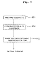
- Fig. 7 shows the outline of the method for producing the optical element according to the present invention.
- a substrate such as a lens is prepared (step S01).
- a buffer film is formed thereon (step S02).
- An optical thin film is formed on the formed buffer film (step S03).
- the optical element is obtained.
- the structure as shown in Fig. 1 was used to prepare a plurality of samples with various film thicknesses of Al 2 O 3 films in each of which the buffer film 3 was the Al 2 O 3 film 2.
- the SiO 2 film 3 had a constant film thickness of 100 nm.
- Fig. 2 shows the optical loss of the entire optical element including the substrate shown in Fig. 1.
- the optical loss is herein represented by (100 - transmittance - reflectance) %.
- the measuring wavelength is 193 nm. It is understood that when the film thickness of the Al 2 O 3 buffer film is 0 nm, i.e., when the SiO 2 optical thin film is directly formed on the CaF 2 substrate, the large loss is exhibited, probably for the following reason. That is, fluorine (F) contained in the substrate and silicon (Si) contained in the optical thin film react with each other by the aid of the large collision energy caused by the sputtering to generate SiF 4 .
- fluorine (F) contained in the substrate and silicon (Si) contained in the optical thin film react with each other by the aid of the large collision energy caused by the sputtering to generate SiF 4 .
- an anti-reflection film of Al 2 O 3 /SiO 2 for a wavelength of 193 was specifically produced.
- An Al 2 O 3 film was formed as the first layer (layer nearest to the substrate) with a film thickness of ⁇ /4 on a CaF 2 substrate.
- ⁇ represents the designed central wavelength of 193 nm.
- the Al 2 O 3 film serves as a high refractive index layer, and it also functions as a buffer film.
- An SiO 2 film was formed to have a film thickness of ⁇ /4 as the second layer.
- the method for forming the film was the ion beam sputtering described above. The entire film formation process was performed in a vacuum chamber at a pressure reduced to be not more than 10 -6 Torr.
- Ar was used as the process gas for the ion source, and the filament was applied with a current and a voltage of 800 V and 40 mA to generate Ar + ion.
- An acceleration voltage of 45 kV was applied to the grid made of carbon.
- Ar which was neutralized by the neutralizer, was radiated onto the target, i.e., toward an Al 2 O 3 target or an SiO 2 target.
- the film formation rate was 0.024 nm/s for Al 2 O 3 and 0.036 nm/s for SiO 2 .
- O 2 was introduced, because the film substance was oxide.
- the film formation was performed at 10 -4 Torr, because the Ar process gas and the O 2 gas were introduced.
- the anti-reflection films of Al 2 O 3 /SiO 2 were formed on both surfaces of the CaF 2 substrate.
- Fig. 3 shows the transmittance of the optical element formed with the film in accordance with the method described above.
- the horizontal axis indicates the measuring wavelength, and the vertical axis indicates the transmittance.
- a good value i.e., a transmittance of 98.6 % was exhibited at a wavelength of 193 nm.
- An Al 2 O 3 buffer film was formed to have a thickness of 8 nm on a CaF 2 substrate having a thickness of 3 mm in accordance with the same method and the condition as those used in Example 1.
- An SiO 2 film was formed to have a thickness of 100 nm on the Al 2 O 3 buffer film to produce an optical element A.
- an SiO 2 film having a thickness of 100 nm was formed on a CaF 2 substrate having a thickness of 3 mm to produce an optical element B in the same manner as in Example 1 except that the Al 2 O 3 buffer film was not formed.
- Fig. 4 shows the change of the transmittance depending on the presence or absence of the buffer film.
- the horizontal axis indicates the wavelength, and the vertical axis indicates the transmittance.
- a solid line indicates the transmittance of the optical element A
- a dotted line indicates the transmittance of the optical element B.
- the wavelength, at which the transmittance of the optical element A exceeds the transmittance of the optical element B ranges from the vicinity of a wavelength of 420 nm. The difference between the both is increased as the wavelength is shorter than the above.
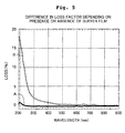
- Fig. 5 shows the change of the loss of the optical element including the substrate depending on the presence or absence of the buffer film.
- the horizontal axis indicates the wavelength, and the vertical axis indicates the loss.
- a solid line indicates the loss of the optical element A
- a dotted line indicates the loss of the optical element B.
- the wavelength, at which the loss of the optical element A is superior to the loss of the optical element B ranges from the vicinity of a wavelength of 780 nm. The difference between the both is increased as the wavelength is longer than the above. According to the results described above, it is understood that the optical element according to the present invention has more excellent optical characteristics than the conventional optical element.
- FIG. 6 conceptually illustrates a scanning type projection exposure apparatus 2000 for exposing a wafer 801 (W as a whole) coated with photoresist 701 with an image of a pattern on a reticle R.
- the optical element produced in Example 1 or 2 can be applied to the exposure apparatus.
- the projection exposure apparatus of the present invention comprises at least a reticle stage 201 which is movable in a direction parallel to the surface of the reticle R while holding the reticle R (mask), a wafer stage 301 which is movable in a direction parallel to the wafer surface while holding the wafer (substrate) W on a surface 301a, an illumination optical system 101 which is provided to irradiate the reticle R (mask) with a vacuum ultraviolet light beam, a light source 100 which is provided to supply the vacuum ultraviolet light beam as the exposure light beam to the illumination optical system 101, and a projection optical system 150 which is provided to project the image of the pattern on the reticle R onto the wafer W.
- the projection optical system 150 is arranged between the reticle R and the wafer W so that the surface P1 on which the reticle R is arranged serves as the object plane, and the surface P2 of the wafer W serves as the image plane.
- the illumination optical system 101 includes an alignment optical system 110 for performing relative positional adjustment for the reticle R and the wafer W.
- a reticle exchange system 200 exchanges and transports the reticle R set to the reticle stage 201.
- the reticle exchange system 200 includes a reticle stage driver (not shown) for moving the reticle stage 201.
- a stage control system 300 is provided with a wafer stage driver (not shown) for moving the wafer stage 301.
- a main control system 400 controls the reticle stage driver and the wafer stage driver by the aid of the stage control system 300 to drive the reticle stage and the wafer stage so that they are synchronously moved with respect to the exposure light beam.
- the projection optical system 150 further includes an alignment optical system 601 to be used for the scanning type exposure apparatus.
- the optical element produced in Example 1 or 2 can be used for the optical lens 90 of the illumination optical system 101 and the projection lens 100 of the projection optical system 150.
- a plurality of projection lenses 100 are arranged in the projection optical system 150.
- the lens, which is disposed on the light-outgoing side, i.e., at the position closest to the wafer W, is the lens according to the present invention.
- the optical thin film may be applied to only the light-incoming plane of the projection lens.
- the optical thin film may be applied to the entire lens.
- the optical elements are used in the exposure apparatus, including, for example, the fly's eye lens, the various relay lenses, the beam splitter, the condenser lens, the beam expander, and the reflecting mirror.
- the present invention is applicable to any element.
- Fig. 6 is illustrative of the scanning type projection exposure apparatus.
- the present invention is not limited thereto.
- the present invention is also applicable to the projection exposure apparatus based on the step-and-repeat system (so-called stepper), the mirror projection aligner, and the proximity type exposure apparatus.
- the optical element equipped with the reflection film can be applied, for example, to a reflecting plate to be used for the exposure apparatus having the projection optical system based on the reflecting system or the cata-dioptric system.
- the projection exposure apparatus and the optical elements used therefor are disclosed in United States Patent No. 5,835,275. This patent document is incorporated herein by reference.
- optical element of the present invention is usable for various apparatuses other than the exposure apparatus, including, for example, spectroscopes, laser repair apparatuses, various inspection apparatuses, and sensors.
- the exposure apparatus of the present invention uses the optical element which has the high transmittance and the low loss. Therefore, it is possible to decrease the loss of illuminance of the exposure light beam until arrival at the substrate as compared with the conventional exposure apparatus.
Landscapes
- Physics & Mathematics (AREA)
- General Physics & Mathematics (AREA)
- Optics & Photonics (AREA)
- Health & Medical Sciences (AREA)
- Engineering & Computer Science (AREA)
- Environmental & Geological Engineering (AREA)
- Epidemiology (AREA)
- Public Health (AREA)
- Toxicology (AREA)
- Exposure Of Semiconductors, Excluding Electron Or Ion Beam Exposure (AREA)
- Exposure And Positioning Against Photoresist Photosensitive Materials (AREA)
- Surface Treatment Of Optical Elements (AREA)
Abstract
Description
Claims (18)
- An optical element (10) having an optical element body (1) which is composed of fluoride, characterized by comprising:;a first layer (2) which is formed on the optical element body and which is composed of a material unreactive with fluorine of the fluoride; anda second layer (3) which is formed on the first layer and which is composed of a material containing silicon.
- The optical element according to claim 1, wherein the first layer is at least one selected from a group consisting of aluminum oxide, hafnium oxide, zirconium oxide, and scandium oxide.
- The optical element according to claim 1, wherein the material containing silicon is silicon oxide.
- The optical element according to claim 1, wherein the fluoride is at least one selected from a group consisting of calcium fluoride, magnesium fluoride, and barium fluoride.
- The optical element according to any one of claims 1 - 4, wherein a film thickness of the first layer is not less than 5 nm.
- The optical element according to claim 1, wherein the first layer is composed of aluminum oxide, and the second layer is composed of silicon oxide.
- An exposure apparatus (2000), for exposing a substrate with an image of a pattern on a mask, which comprises an illumination optical system (101) which illuminates the mask with vacuum ultraviolet light and a projection optical system (150) which includes an optical element (100) and which projects the image of the pattern on the mask onto the substrate, characterized in that:the optical element (100) comprises an optical element body (1) which is composed of fluoride; a first layer (2) which is formed on the optical element body and which is composed of a material unreactive with fluorine of the fluoride; and a second layer (3) which is formed on the first layer and which is composed of a material containing silicon.
- The exposure apparatus according to claim 7, wherein the first layer of the optical element is formed of aluminum oxide, and the second layer is composed of silicon oxide.
- The exposure apparatus according to claim 7 or 8, wherein the vacuum ultraviolet light has a wavelength of not
- An exposure apparatus, for exposing a substrate with an image of a pattern on a mask, which comprises an illumination optical system (101) which includes an optical element (90) and which illuminates the mask with vacuum ultraviolet light and a projection optical system which projects the image of the pattern on the mask onto the substrate, characterized in that:the optical element (90) comprises an optical element body (1) which is composed of fluoride; a first layer (2) which is formed on the optical element body and which is composed of a material unreactive with fluorine of the fluoride; and a second layer (3) which is formed on the first layer and which is composed of a material containing silicon.
- The exposure apparatus according to claim 10, wherein the first layer of the optical element is formed of aluminum oxide, and the second layer is composed of silicon oxide.
- The exposure apparatus according to claim 10 or 11, wherein the vacuum ultraviolet light has a wavelength of not more than 250 nm.
- A method for producing an optical element (10), comprising:forming, on an optical element body (1) composed of fluoride, a first layer (2) composed of a material unreactive with fluorine of the fluoride; andforming, on the first layer, a second layer (3) composed of a material containing silicon.
- The method for producing the optical element according to claim 13, wherein at least one of the first layer and the second layer is formed by means of sputtering.
- The method for producing the optical element according to claim 13, wherein the first layer is at least one selected from a group consisting of aluminum oxide, hafnium oxide, zirconium oxide, and scandium oxide.
- The method for producing the optical element according to claim 14, wherein the material containing silicon is silicon oxide.
- The method for producing the optical element according to any one of claims 13 - 16, wherein the fluoride is at least one selected from a group consisting of calcium fluoride, magnesium fluoride, and barium fluoride.
- The method for producing the optical element according to claim 13, wherein the first layer is formed with a film thickness of not less than 5 nm.
Applications Claiming Priority (2)
| Application Number | Priority Date | Filing Date | Title |
|---|---|---|---|
| JP2000209600 | 2000-07-11 | ||
| JP2000209600 | 2000-07-11 |
Publications (2)
| Publication Number | Publication Date |
|---|---|
| EP1172670A2 true EP1172670A2 (en) | 2002-01-16 |
| EP1172670A3 EP1172670A3 (en) | 2003-07-16 |
Family
ID=18705979
Family Applications (1)
| Application Number | Title | Priority Date | Filing Date |
|---|---|---|---|
| EP01115800A Withdrawn EP1172670A3 (en) | 2000-07-11 | 2001-07-11 | Optical element formed with optical thin film and ultraviolet exposure apparatus |
Country Status (2)
| Country | Link |
|---|---|
| US (1) | US20020005990A1 (en) |
| EP (1) | EP1172670A3 (en) |
Cited By (8)
| Publication number | Priority date | Publication date | Assignee | Title |
|---|---|---|---|---|
| EP1571700A4 (en) * | 2002-12-10 | 2007-09-12 | Nikon Corp | OPTICAL DEVICE AND APPARATUS FOR PROJECTING AMBIENCE USING SUCH AN OPTICAL DEVICE |
| US7366699B1 (en) | 1999-03-05 | 2008-04-29 | Sony Corporation | Electronic money system, electronic money terminal device, and information card |
| US7440206B2 (en) | 2004-04-29 | 2008-10-21 | Mitsubishi Heavy Industries, Ltd. | Optical properties restoration apparatus, the restoration method, and an optical system used in the apparatus |
| US7924397B2 (en) | 2003-11-06 | 2011-04-12 | Taiwan Semiconductor Manufacturing Company, Ltd. | Anti-corrosion layer on objective lens for liquid immersion lithography applications |
| US7993008B2 (en) | 2003-08-26 | 2011-08-09 | Nikon Corporation | Optical element and exposure apparatus |
| US8149381B2 (en) | 2003-08-26 | 2012-04-03 | Nikon Corporation | Optical element and exposure apparatus |
| US8208123B2 (en) | 2003-08-29 | 2012-06-26 | Asml Netherlands B.V. | Lithographic apparatus and device manufacturing method |
| CN101656187B (en) * | 2004-05-31 | 2013-06-19 | 三菱重工业株式会社 | Optical performance recovery device, recovery method and optical system used for the device |
Families Citing this family (5)
| Publication number | Priority date | Publication date | Assignee | Title |
|---|---|---|---|---|
| FR2773261B1 (en) | 1997-12-30 | 2000-01-28 | Commissariat Energie Atomique | METHOD FOR THE TRANSFER OF A THIN FILM COMPRISING A STEP OF CREATING INCLUSIONS |
| JP4006226B2 (en) * | 2001-11-26 | 2007-11-14 | キヤノン株式会社 | Optical element manufacturing method, optical element, exposure apparatus, device manufacturing method, and device |
| US6824654B2 (en) * | 2002-10-01 | 2004-11-30 | Asml Holding N.V. | Method of making a cube |
| FR2922359B1 (en) * | 2007-10-12 | 2009-12-18 | Commissariat Energie Atomique | METHOD FOR MANUFACTURING A MICROELECTRONIC STRUCTURE INVOLVING MOLECULAR COLLAGE |
| US20090244507A1 (en) * | 2008-03-28 | 2009-10-01 | Nikon Corporation | Optical member, light routing unit, and exposure apparatus |
Family Cites Families (4)
| Publication number | Priority date | Publication date | Assignee | Title |
|---|---|---|---|---|
| JPH08220304A (en) * | 1995-02-13 | 1996-08-30 | Tadahiro Omi | Optical article, exposure apparatus or optical system using the same, and method of manufacturing the same |
| JP3689524B2 (en) * | 1996-03-22 | 2005-08-31 | キヤノン株式会社 | Aluminum oxide film and method for forming the same |
| JPH11311704A (en) * | 1998-02-26 | 1999-11-09 | Nikon Corp | UV light mirror |
| EP1152263A4 (en) * | 1999-09-30 | 2003-08-20 | Nikon Corp | OPTICAL DEVICE WITH THIN MULTI-LAYER SYSTEM AND THEIR USE FOR ALIGNMENT |
-
2001
- 2001-07-10 US US09/901,015 patent/US20020005990A1/en not_active Abandoned
- 2001-07-11 EP EP01115800A patent/EP1172670A3/en not_active Withdrawn
Cited By (17)
| Publication number | Priority date | Publication date | Assignee | Title |
|---|---|---|---|---|
| US7366699B1 (en) | 1999-03-05 | 2008-04-29 | Sony Corporation | Electronic money system, electronic money terminal device, and information card |
| US8767173B2 (en) | 2002-12-10 | 2014-07-01 | Nikon Corporation | Optical element and projection exposure apparatus based on use of the optical element |
| EP1571700A4 (en) * | 2002-12-10 | 2007-09-12 | Nikon Corp | OPTICAL DEVICE AND APPARATUS FOR PROJECTING AMBIENCE USING SUCH AN OPTICAL DEVICE |
| US7876418B2 (en) | 2002-12-10 | 2011-01-25 | Nikon Corporation | Optical element and projection exposure apparatus based on use of the optical element |
| US8149381B2 (en) | 2003-08-26 | 2012-04-03 | Nikon Corporation | Optical element and exposure apparatus |
| US10175584B2 (en) | 2003-08-26 | 2019-01-08 | Nikon Corporation | Optical element and exposure apparatus |
| US9046796B2 (en) | 2003-08-26 | 2015-06-02 | Nikon Corporation | Optical element and exposure apparatus |
| US8189170B2 (en) | 2003-08-26 | 2012-05-29 | Nikon Corporation | Optical element and exposure apparatus |
| US7993008B2 (en) | 2003-08-26 | 2011-08-09 | Nikon Corporation | Optical element and exposure apparatus |
| US8208123B2 (en) | 2003-08-29 | 2012-06-26 | Asml Netherlands B.V. | Lithographic apparatus and device manufacturing method |
| US8179516B2 (en) * | 2003-11-06 | 2012-05-15 | Taiwan Semiconductor Manufacturing Company, Ltd. | Protective layer on objective lens for liquid immersion lithography applications |
| US7924397B2 (en) | 2003-11-06 | 2011-04-12 | Taiwan Semiconductor Manufacturing Company, Ltd. | Anti-corrosion layer on objective lens for liquid immersion lithography applications |
| US7813036B2 (en) | 2004-04-29 | 2010-10-12 | Mitsubishi Heavy Industries, Ltd. | Optical properties restoration apparatus, the restoration method, and an optical system used in the apparatus |
| US7733563B2 (en) | 2004-04-29 | 2010-06-08 | Mitsubishi Heavy Industries, Ltd. | Optical properties restoration apparatus, the restoration method, and an optical system used in the apparatus |
| US7453630B2 (en) | 2004-04-29 | 2008-11-18 | Mitsubishi Heavy Industries, Ltd. | Optical properties apparatus, the restoration method, and an optical system used in the apparatus |
| US7440206B2 (en) | 2004-04-29 | 2008-10-21 | Mitsubishi Heavy Industries, Ltd. | Optical properties restoration apparatus, the restoration method, and an optical system used in the apparatus |
| CN101656187B (en) * | 2004-05-31 | 2013-06-19 | 三菱重工业株式会社 | Optical performance recovery device, recovery method and optical system used for the device |
Also Published As
| Publication number | Publication date |
|---|---|
| US20020005990A1 (en) | 2002-01-17 |
| EP1172670A3 (en) | 2003-07-16 |
Similar Documents
| Publication | Publication Date | Title |
|---|---|---|
| US7998645B2 (en) | Method for finishing surface of preliminary polished glass substrate | |
| US7459707B2 (en) | Exposure apparatus, light source apparatus and device fabrication | |
| US20050024610A1 (en) | Exposure apparatus and stage device, and device manufacturing method | |
| JP3495992B2 (en) | Correction apparatus, exposure apparatus, device manufacturing method and device | |
| EP1452921A1 (en) | Projection exposure method and apparatus and device manufacturing method | |
| US20020005990A1 (en) | Optical element formed with optical thin film and exposure apparatus | |
| EP1152263A1 (en) | Optical device with multilayer thin film and aligner with the device | |
| US8064042B2 (en) | Exposure apparatus and device fabrication method | |
| TW201011477A (en) | Mirror, lithographic apparatus and device manufacturing method | |
| US20090004374A1 (en) | Mirror and exposure apparatus having the same | |
| JP2000133588A (en) | Exposure apparatus and method, manufacturing method of the exposure apparatus, and device manufacturing method using the exposure apparatus | |
| JP2003124095A (en) | Projection exposure method and apparatus, and device manufacturing method | |
| JP3352325B2 (en) | Scanning exposure apparatus and device manufacturing method using the same | |
| US6172739B1 (en) | Exposure apparatus and method | |
| US7170683B2 (en) | Reflection element of exposure light and production method therefor, mask, exposure system, and production method of semiconductor device | |
| JP2005209769A (en) | Exposure equipment | |
| US8179520B2 (en) | Optical element, projection optical system, exposure apparatus, and device fabrication method | |
| US7060994B2 (en) | Exposure apparatus and method | |
| JP2002115047A (en) | Method for forming optical thin film, optical thin film, optical element, and exposure apparatus | |
| US7295367B2 (en) | Optical element, optical apparatus, film forming method, film forming apparatus and device fabrication method | |
| JP2000100721A (en) | Scanning exposure method, scanning exposure apparatus, and device manufacturing method | |
| JPH1164778A (en) | Illumination optics | |
| JP4819419B2 (en) | Imaging optical system, exposure apparatus, and device manufacturing method | |
| JP2001118784A (en) | EXPOSURE APPARATUS, METHOD OF CORRECTION OF DENSITY AND DENSITY LINE WIDTH IN THE EXPOSURE APPARATUS AND EXPOSURE METHOD | |
| JP2005257769A (en) | Optical thin film, optical element, and exposure apparatus and exposure method using the same |
Legal Events
| Date | Code | Title | Description |
|---|---|---|---|
| PUAI | Public reference made under article 153(3) epc to a published international application that has entered the european phase |
Free format text: ORIGINAL CODE: 0009012 |
|
| AK | Designated contracting states |
Kind code of ref document: A2 Designated state(s): AT BE CH CY DE DK ES FI FR GB GR IE IT LI LU MC NL PT SE TR |
|
| AX | Request for extension of the european patent |
Free format text: AL;LT;LV;MK;RO;SI |
|
| PUAL | Search report despatched |
Free format text: ORIGINAL CODE: 0009013 |
|
| AK | Designated contracting states |
Designated state(s): AT BE CH CY DE DK ES FI FR GB GR IE IT LI LU MC NL PT SE TR |
|
| AX | Request for extension of the european patent |
Extension state: AL LT LV MK RO SI |
|
| RIC1 | Information provided on ipc code assigned before grant |
Ipc: 7G 02B 1/11 B Ipc: 7G 02B 13/14 B Ipc: 7G 02B 1/10 A |
|
| STAA | Information on the status of an ep patent application or granted ep patent |
Free format text: STATUS: THE APPLICATION HAS BEEN WITHDRAWN |
|
| 18W | Application withdrawn |
Effective date: 20031010 |