EP1170129A2 - Inkjet printhead and method of fabricating an inkjet printhead - Google Patents
Inkjet printhead and method of fabricating an inkjet printhead Download PDFInfo
- Publication number
- EP1170129A2 EP1170129A2 EP01305328A EP01305328A EP1170129A2 EP 1170129 A2 EP1170129 A2 EP 1170129A2 EP 01305328 A EP01305328 A EP 01305328A EP 01305328 A EP01305328 A EP 01305328A EP 1170129 A2 EP1170129 A2 EP 1170129A2
- Authority
- EP
- European Patent Office
- Prior art keywords
- dielectric material
- vias
- dielectric
- layer
- resistive
- Prior art date
- Legal status (The legal status is an assumption and is not a legal conclusion. Google has not performed a legal analysis and makes no representation as to the accuracy of the status listed.)
- Granted
Links
- 238000004519 manufacturing process Methods 0.000 title claims abstract description 13
- 239000003989 dielectric material Substances 0.000 claims abstract description 80
- 239000004020 conductor Substances 0.000 claims abstract description 74
- 238000000034 method Methods 0.000 claims abstract description 54
- 239000000463 material Substances 0.000 claims abstract description 50
- 229920002120 photoresistant polymer Polymers 0.000 claims abstract description 35
- 238000002161 passivation Methods 0.000 claims abstract description 26
- 230000004888 barrier function Effects 0.000 claims description 17
- 238000000151 deposition Methods 0.000 claims description 9
- RYGMFSIKBFXOCR-UHFFFAOYSA-N Copper Chemical compound [Cu] RYGMFSIKBFXOCR-UHFFFAOYSA-N 0.000 claims description 7
- BOTDANWDWHJENH-UHFFFAOYSA-N Tetraethyl orthosilicate Chemical compound CCO[Si](OCC)(OCC)OCC BOTDANWDWHJENH-UHFFFAOYSA-N 0.000 claims description 7
- 229910052802 copper Inorganic materials 0.000 claims description 7
- 239000010949 copper Substances 0.000 claims description 7
- 238000005530 etching Methods 0.000 claims description 7
- 229910052782 aluminium Inorganic materials 0.000 claims description 6
- XAGFODPZIPBFFR-UHFFFAOYSA-N aluminium Chemical compound [Al] XAGFODPZIPBFFR-UHFFFAOYSA-N 0.000 claims description 6
- 238000001312 dry etching Methods 0.000 claims description 4
- 238000010438 heat treatment Methods 0.000 claims description 4
- 238000001039 wet etching Methods 0.000 claims 1
- 239000010410 layer Substances 0.000 description 145
- 238000010304 firing Methods 0.000 description 20
- 239000010409 thin film Substances 0.000 description 14
- 230000036961 partial effect Effects 0.000 description 12
- 238000005240 physical vapour deposition Methods 0.000 description 7
- 238000009413 insulation Methods 0.000 description 5
- XUIMIQQOPSSXEZ-UHFFFAOYSA-N Silicon Chemical group [Si] XUIMIQQOPSSXEZ-UHFFFAOYSA-N 0.000 description 4
- 239000012530 fluid Substances 0.000 description 4
- 238000000623 plasma-assisted chemical vapour deposition Methods 0.000 description 4
- 229910052710 silicon Inorganic materials 0.000 description 4
- 239000010703 silicon Substances 0.000 description 4
- WFKWXMTUELFFGS-UHFFFAOYSA-N tungsten Chemical compound [W] WFKWXMTUELFFGS-UHFFFAOYSA-N 0.000 description 4
- 229910052721 tungsten Inorganic materials 0.000 description 4
- 239000010937 tungsten Substances 0.000 description 4
- VYPSYNLAJGMNEJ-UHFFFAOYSA-N Silicium dioxide Chemical class O=[Si]=O VYPSYNLAJGMNEJ-UHFFFAOYSA-N 0.000 description 3
- 229920000642 polymer Polymers 0.000 description 3
- 238000007639 printing Methods 0.000 description 3
- 239000000758 substrate Substances 0.000 description 3
- 229910052715 tantalum Inorganic materials 0.000 description 3
- GUVRBAGPIYLISA-UHFFFAOYSA-N tantalum atom Chemical compound [Ta] GUVRBAGPIYLISA-UHFFFAOYSA-N 0.000 description 3
- 229910052581 Si3N4 Inorganic materials 0.000 description 2
- RTAQQCXQSZGOHL-UHFFFAOYSA-N Titanium Chemical compound [Ti] RTAQQCXQSZGOHL-UHFFFAOYSA-N 0.000 description 2
- -1 aluminum gold Chemical compound 0.000 description 2
- 238000004891 communication Methods 0.000 description 2
- 238000007641 inkjet printing Methods 0.000 description 2
- 150000002500 ions Chemical class 0.000 description 2
- 230000000873 masking effect Effects 0.000 description 2
- 229910052751 metal Inorganic materials 0.000 description 2
- 239000002184 metal Substances 0.000 description 2
- 239000000203 mixture Substances 0.000 description 2
- 238000000206 photolithography Methods 0.000 description 2
- HBMJWWWQQXIZIP-UHFFFAOYSA-N silicon carbide Chemical compound [Si+]#[C-] HBMJWWWQQXIZIP-UHFFFAOYSA-N 0.000 description 2
- 229910010271 silicon carbide Inorganic materials 0.000 description 2
- 235000012239 silicon dioxide Nutrition 0.000 description 2
- HQVNEWCFYHHQES-UHFFFAOYSA-N silicon nitride Chemical compound N12[Si]34N5[Si]62N3[Si]51N64 HQVNEWCFYHHQES-UHFFFAOYSA-N 0.000 description 2
- 239000000126 substance Substances 0.000 description 2
- 229910052719 titanium Inorganic materials 0.000 description 2
- 239000010936 titanium Substances 0.000 description 2
- 230000004913 activation Effects 0.000 description 1
- 230000006978 adaptation Effects 0.000 description 1
- RVSGESPTHDDNTH-UHFFFAOYSA-N alumane;tantalum Chemical compound [AlH3].[Ta] RVSGESPTHDDNTH-UHFFFAOYSA-N 0.000 description 1
- 230000007797 corrosion Effects 0.000 description 1
- 238000005260 corrosion Methods 0.000 description 1
- 230000003247 decreasing effect Effects 0.000 description 1
- 239000011521 glass Substances 0.000 description 1
- 239000012212 insulator Substances 0.000 description 1
- 238000003475 lamination Methods 0.000 description 1
- 238000002789 length control Methods 0.000 description 1
- 230000000670 limiting effect Effects 0.000 description 1
- 239000000615 nonconductor Substances 0.000 description 1
- 230000006911 nucleation Effects 0.000 description 1
- 238000010899 nucleation Methods 0.000 description 1
- 229920000620 organic polymer Polymers 0.000 description 1
- 239000011241 protective layer Substances 0.000 description 1
- 230000002000 scavenging effect Effects 0.000 description 1
- 239000000377 silicon dioxide Substances 0.000 description 1
- 238000004544 sputter deposition Methods 0.000 description 1
- 238000003860 storage Methods 0.000 description 1
Images


Classifications
-
- B—PERFORMING OPERATIONS; TRANSPORTING
- B41—PRINTING; LINING MACHINES; TYPEWRITERS; STAMPS
- B41J—TYPEWRITERS; SELECTIVE PRINTING MECHANISMS, i.e. MECHANISMS PRINTING OTHERWISE THAN FROM A FORME; CORRECTION OF TYPOGRAPHICAL ERRORS
- B41J2/00—Typewriters or selective printing mechanisms characterised by the printing or marking process for which they are designed
- B41J2/005—Typewriters or selective printing mechanisms characterised by the printing or marking process for which they are designed characterised by bringing liquid or particles selectively into contact with a printing material
- B41J2/01—Ink jet
- B41J2/135—Nozzles
- B41J2/16—Production of nozzles
- B41J2/1621—Manufacturing processes
- B41J2/1626—Manufacturing processes etching
- B41J2/1629—Manufacturing processes etching wet etching
-
- B—PERFORMING OPERATIONS; TRANSPORTING
- B41—PRINTING; LINING MACHINES; TYPEWRITERS; STAMPS
- B41J—TYPEWRITERS; SELECTIVE PRINTING MECHANISMS, i.e. MECHANISMS PRINTING OTHERWISE THAN FROM A FORME; CORRECTION OF TYPOGRAPHICAL ERRORS
- B41J2/00—Typewriters or selective printing mechanisms characterised by the printing or marking process for which they are designed
- B41J2/005—Typewriters or selective printing mechanisms characterised by the printing or marking process for which they are designed characterised by bringing liquid or particles selectively into contact with a printing material
- B41J2/01—Ink jet
- B41J2/135—Nozzles
- B41J2/14—Structure thereof only for on-demand ink jet heads
- B41J2/14016—Structure of bubble jet print heads
- B41J2/14088—Structure of heating means
- B41J2/14112—Resistive element
- B41J2/14129—Layer structure
-
- B—PERFORMING OPERATIONS; TRANSPORTING
- B41—PRINTING; LINING MACHINES; TYPEWRITERS; STAMPS
- B41J—TYPEWRITERS; SELECTIVE PRINTING MECHANISMS, i.e. MECHANISMS PRINTING OTHERWISE THAN FROM A FORME; CORRECTION OF TYPOGRAPHICAL ERRORS
- B41J2/00—Typewriters or selective printing mechanisms characterised by the printing or marking process for which they are designed
- B41J2/005—Typewriters or selective printing mechanisms characterised by the printing or marking process for which they are designed characterised by bringing liquid or particles selectively into contact with a printing material
- B41J2/01—Ink jet
- B41J2/135—Nozzles
- B41J2/16—Production of nozzles
- B41J2/1601—Production of bubble jet print heads
- B41J2/1603—Production of bubble jet print heads of the front shooter type
-
- B—PERFORMING OPERATIONS; TRANSPORTING
- B41—PRINTING; LINING MACHINES; TYPEWRITERS; STAMPS
- B41J—TYPEWRITERS; SELECTIVE PRINTING MECHANISMS, i.e. MECHANISMS PRINTING OTHERWISE THAN FROM A FORME; CORRECTION OF TYPOGRAPHICAL ERRORS
- B41J2/00—Typewriters or selective printing mechanisms characterised by the printing or marking process for which they are designed
- B41J2/005—Typewriters or selective printing mechanisms characterised by the printing or marking process for which they are designed characterised by bringing liquid or particles selectively into contact with a printing material
- B41J2/01—Ink jet
- B41J2/135—Nozzles
- B41J2/16—Production of nozzles
- B41J2/1621—Manufacturing processes
- B41J2/1626—Manufacturing processes etching
- B41J2/1628—Manufacturing processes etching dry etching
-
- B—PERFORMING OPERATIONS; TRANSPORTING
- B41—PRINTING; LINING MACHINES; TYPEWRITERS; STAMPS
- B41J—TYPEWRITERS; SELECTIVE PRINTING MECHANISMS, i.e. MECHANISMS PRINTING OTHERWISE THAN FROM A FORME; CORRECTION OF TYPOGRAPHICAL ERRORS
- B41J2/00—Typewriters or selective printing mechanisms characterised by the printing or marking process for which they are designed
- B41J2/005—Typewriters or selective printing mechanisms characterised by the printing or marking process for which they are designed characterised by bringing liquid or particles selectively into contact with a printing material
- B41J2/01—Ink jet
- B41J2/135—Nozzles
- B41J2/16—Production of nozzles
- B41J2/1621—Manufacturing processes
- B41J2/1631—Manufacturing processes photolithography
-
- B—PERFORMING OPERATIONS; TRANSPORTING
- B41—PRINTING; LINING MACHINES; TYPEWRITERS; STAMPS
- B41J—TYPEWRITERS; SELECTIVE PRINTING MECHANISMS, i.e. MECHANISMS PRINTING OTHERWISE THAN FROM A FORME; CORRECTION OF TYPOGRAPHICAL ERRORS
- B41J2/00—Typewriters or selective printing mechanisms characterised by the printing or marking process for which they are designed
- B41J2/005—Typewriters or selective printing mechanisms characterised by the printing or marking process for which they are designed characterised by bringing liquid or particles selectively into contact with a printing material
- B41J2/01—Ink jet
- B41J2/135—Nozzles
- B41J2/16—Production of nozzles
- B41J2/1621—Manufacturing processes
- B41J2/1632—Manufacturing processes machining
-
- B—PERFORMING OPERATIONS; TRANSPORTING
- B41—PRINTING; LINING MACHINES; TYPEWRITERS; STAMPS
- B41J—TYPEWRITERS; SELECTIVE PRINTING MECHANISMS, i.e. MECHANISMS PRINTING OTHERWISE THAN FROM A FORME; CORRECTION OF TYPOGRAPHICAL ERRORS
- B41J2/00—Typewriters or selective printing mechanisms characterised by the printing or marking process for which they are designed
- B41J2/005—Typewriters or selective printing mechanisms characterised by the printing or marking process for which they are designed characterised by bringing liquid or particles selectively into contact with a printing material
- B41J2/01—Ink jet
- B41J2/135—Nozzles
- B41J2/16—Production of nozzles
- B41J2/1621—Manufacturing processes
- B41J2/164—Manufacturing processes thin film formation
- B41J2/1642—Manufacturing processes thin film formation thin film formation by CVD [chemical vapor deposition]
-
- B—PERFORMING OPERATIONS; TRANSPORTING
- B41—PRINTING; LINING MACHINES; TYPEWRITERS; STAMPS
- B41J—TYPEWRITERS; SELECTIVE PRINTING MECHANISMS, i.e. MECHANISMS PRINTING OTHERWISE THAN FROM A FORME; CORRECTION OF TYPOGRAPHICAL ERRORS
- B41J2/00—Typewriters or selective printing mechanisms characterised by the printing or marking process for which they are designed
- B41J2/005—Typewriters or selective printing mechanisms characterised by the printing or marking process for which they are designed characterised by bringing liquid or particles selectively into contact with a printing material
- B41J2/01—Ink jet
- B41J2/135—Nozzles
- B41J2/16—Production of nozzles
- B41J2/1621—Manufacturing processes
- B41J2/164—Manufacturing processes thin film formation
- B41J2/1646—Manufacturing processes thin film formation thin film formation by sputtering
Abstract
Description
- This invention relates to the manufacturer of printheads used in inkjet printers, and more specifically to an inkjet printhead used in an inkjet print cartridge having improved dimensional control and improved step coverage.
- One type of inkjet printing system uses a piezoelectric transducer to produce a pressure pulse that expels a droplet of ink from a nozzle. A second type of inkjet printing system uses thermal energy to produce a vapor bubble in an ink-filled chamber that expels a droplet of ink. The second type is referred to as thermal inkjet or bubble jet printing systems.
- Conventional thermal inkjet printers include a print cartridge in which small droplets of ink are formed and ejected towards a printing medium. Such print cartridges include inkjet printheads with orifice plates having very small nozzles through which the ink droplets are ejected. Adjacent to the nozzles inside the inkjet printhead are ink chambers, where ink is stored prior to ejection. Ink is delivered to the ink chambers through ink channels that are in fluid communication with an ink supply. The ink supply may be, for example, contained in a reservoir part of the print cartridge.
- Ejection of an ink droplet through a nozzle may be accomplished by quickly heating a volume of ink within the adjacent ink chamber. The rapid expansion of ink vapor forces a drop of ink through the nozzle. This process is commonly known as "firing." The ink in the chamber may be heated with a transducer, such as a resistor, that is aligned adjacent to the nozzle.
- In conventional thermal inkjet printhead devices, thin film resistors are used as heating elements. In such thin film devices, the resistive heating material is typically deposited on a thermally and electrically insulating substrate. A conductive layer is then deposited over the resistive material. The individual heater element (i.e., resistor) is dimensionally defined by conductive trace patterns that are lithographically formed through numerous steps including conventionally masking, ultraviolet exposure, and etching techniques on the conductive and resistive layers. More specifically, the critical width dimension of an individual resistor is controlled by a dry etch process. For example, a reactive ion etch process is used to etch portions of the conductive layer not protected by a photoresist mask. The conductive layer is removed and a portion of the resistive layer is exposed. The resistive width is defined as the width of the exposed resistive layer between the vertical walls of the conductive layer. Conversely, the critical length dimension of an individual resistor is controlled by a subsequent wet etch process. A wet etch process is used to produce a resistor having sloped walls defining the resistor length. Sloped walls of a resistor permit step coverage of later fabricated layers.
- As discussed above, conventional thermal inkjet printhead devices require both dry etch and wet etch processes. The dry etch process determines the width dimension of an individual resistor, while the wet etch process defines both the length dimension and the necessary sloped walls of the individual resistor. As is well known in the art, each process requires numerous steps, thereby increasing both the time to manufacture a printhead device and the cost of manufacturing a printhead device.
- One or more passivation and cavitation layers are fabricated over the conductive and resistive layers and then selectively removed to create a via for electrical connection of a second conductive layer to the conductive traces. The second conductive layer is pattered to define a discrete conductive path from each trace to an exposed bonding pad remote from the resistor. The bonding pad facilitates connection with electrical contacts on the print cartridge. Activation signals are provided from the printer to the resistor via the electrical contacts.
- The printhead substructure is overlaid with an ink barrier layer. The ink barrier layer is etched to define the shape of the desired firing chamber within the ink barrier layer. The firing chamber is situated above, and aligned with, the resistor. The ink barrier layer includes a nozzle print cartridge adjacent to each firing chamber.
- In direct drive thermal inkjet printer designs, the thin film device is selectively driven by the above-described thermal electric integrated circuit part of the printhead substructure. The integrated circuit conducts electrical signals directly from the printer microprocessor to the resistor via the two conductive layers. The resistor increases in temperature and creates super-heated ink bubbles for ejection from the chamber through the nozzle. However, conventional thermal inkjet printhead devices suffer from inconsistent and unreliable ink drop sizes and inconsistent turn on energy required to fire an ink droplet.
- It is desirous to fabricate an inkjet printhead capable of producing ink droplets having consistent and reliable ink drop sizes. In addition, it is desirous to fabricate an inkjet printhead having a consistent low turn on energy (TOE) required to fire an ink droplet, thereby providing greater control of the size of the ink drops.
- The present invention includes an inkjet printhead and a method of fabricating an inkjet printhead. One method of the present invention includes fabricating first and second conductors having a space therebetween. A dielectric material is fabricated on top of the first and second conductors and in the space between the conductors. First and second vias are formed in the dielectric material adjacent the first and second conductors, respectively. A resistive material layer is fabricated on top of the dielectric material such that a first electrical connection is formed with the first conductor and a second electrical connection is formed with the second conductor. In one embodiment of the present invention, the first and second conductors are electrically connected to circuitry capable of providing energy to the resistive material layer such that an ink droplet can be fired in a direction substantially perpendicular to the resistive material layer.
- In another embodiment of the present invention, an inkjet printhead includes first and second conductors having a space formed therebetween. A dielectric material is fabricated between the first and second conductors and a resistive material layer. A first via is formed in the dielectric material between the first conductor and the resistive material layer such that a first electrical connection is formed between the first conductor and the resistive material layer. A second via is formed in the dielectric material between the second conductor and the resistive material layer such that a second electrical connection is formed between the second conductor and the resistive material layer.
- Another method of present invention includes depositing a conducting material layer onto an insulative dielectric. A portion of the conducting material layer is removed, thereby developing a chamber between first and second conductors. A dielectric material is deposited onto the first and second conductors and onto the insulative dielectric in the chamber. A top surface of the dielectric material is planarized. First and second vias are etched through the dielectric material to expose a portion of the first and second conductors, respectively. In one preferred embodiment, the first and second vias are simultaneously etched through a wet or a dry etch process. The side walls of the first and second vias in the dielectric material are etched such that they are sloped at an angle in the range of approximately 10-60 degrees. A resistive material layer is fabricated within the first and second vias and on the planarized dielectric material between the first and second vias. A passivation material layer is deposited onto the dielectric material and the resistive material layer.
- In one embodiment of the present invention, the steps of etching the first and second vias through the dielectric material further include depositing and defining a photoresist mask through standard photolithography techniques. The photoresist mask is subject to a high temperature bake process thereby creating sloped or concave portions of the photoresist mask such that portions of the dielectric material are exposed. The exposed portions of the dielectric material are etched through a dry etch process, thereby creating the first and second vias in the dielectric material having walls sloped in the range of 10-60 degrees. The remaining portion of the photoresist mask is then removed.
- In another embodiment, the vias having sloped walls are formed through a photoresist mask which is deposited and defined, and a dry etch process which changes the selectivity of etch rate between the photoresist mask and the dielectric material resulting in a sloped profile. In yet another embodiment, the vias having sloped walls are formed through a photoresist mask and a wet etch process.
- With reference to the resistive layer, a photoresist mask is deposited and defined onto a portion of the resistive material layer corresponding to a resistor element. The exposed portion of the resistive material layer is etched. The photoresist mask is removed, thereby exposing the resistive element having a length at least as great as the distance between the outermost potions of the first and second vias in the dielectric material.
- In yet another embodiment of the present invention, an inkjet printhead includes an insulative dielectric. First and second conductors are fabricated on the insulative dielectric having a chamber formed therebetween, the first and second conductors each having a width. The inkjet printhead also includes a dielectric material fabricated on the first and second conductors and on the insulative dielectric in the chamber. Further, first and second vias are formed in the dielectric material, thereby exposing a portion of the first and second conductors, respectively. The first and second vias formed in the dielectric material have side walls sloped at an angle in the range of approximately 10-60 degrees. Further, a resistive material layer is formed within the first and second vias and on the dielectric material between the first and second vias. The resistive material layer has a length greater than a distance between the outermost portions of the first and second vias in the dielectric material and has a maximum width equal to the width of the first and second conductors. Further, a passivation material layer is formed on the dielectric material and on the resistive material layer.
- In one embodiment of the inkjet printhead, the conducting material layer includes up to 2.0 percent copper in aluminum, while in other embodiments, the conducting material layer is formed from titanium or tungsten. Further, the dielectric material is fabricated from tetraethylorthosilicate (TEOS) oxide. In another embodiment, the passivation material layer is a silicon-containing layer. In yet another embodiment, the passivation material layer is a dielectric layer.
- In one embodiment, the insulative dielectric is capable of dissipating heat. In another embodiment, the inkjet printhead apparatus includes an ink barrier layer having a chamber formed therein, the chamber located above the resistive layer and between the first and second vias. Further, in yet another embodiment, the inkjet printhead apparatus includes a fill layer, such as a conductive material layer or a dielectric layer, formed in the first and second vias prior to forming the resistive material layer.
- The present invention provides numerous advantages over the prior art. First, the present invention provides a design capable of firing an ink droplet in a direction substantially perpendicular to the resistive element. Second, the dimensions and planarity of the resistive material layer are precisely controlled, which both standardizes and minimizes the turn on energy required to fire an ink droplet. Third, the size of an ink droplet can be standardized for optimal quality and consistency.
- The present invention achieves the above discussed advantages by forming vias in a dielectric material to provide an electrical connection between first and second conductors and a resistive material layer. The present invention further utilizes a single mask and a single etch to fabricate the resistive material layer, rather than using both a dry and a wet etch process as is known in the prior art. The vias of the present invention are formed having desired sloped walls which facilitate enhanced step coverage of subsequent layers. The resistive material layer is precisely designed on top of the dielectric material.
-
- Figure 1 is a perspective view of an inkjet printer print cartridge.
- Figure 2 is an enlarged, cross-sectional, partial view illustrating a thin film printhead substructure.
- Figure 3 is an enlarged, cross-sectional, partial view illustrating a thin film printhead substructure.
- Figures 4 and 5A are enlarged, cross-sectional, partial views illustrating various fabrication steps of the present invention.
- Figure 5B is an enlarged, plan view illustrating a portion of the cross-sectional view shown in Figure 5A.
- Figures 6-9A are enlarged, cross-sectional, partial views illustrating various fabrication steps of the present invention.
- Figure 9B is an enlarged, plane view illustrating a portion of the cross-sectional view shown in Figure 9A.
- Figure 9C is an enlarged, cross-sectional, partial view illustrating a portion of the cross-sectional view shown in Figure 9A.
- Figure 10A is an enlarged, cross-sectional, partial view illustrating a fabrication step of the present invention.
- Figure 10B is an enlarged, plane view illustrating a portion of the cross-sectional view shown in Figure 10A.
- Figure 11 is an enlarged, cross-sectional, partial view illustrating an alternate embodiment of the present invention.
- Figures 12 and 13 are enlarged, cross-sectional, partial views illustrating various fabrication steps of the present invention.
-
- In the following detailed description of the preferred embodiments, reference is made to the accompanying drawings which form a part hereof, and in which is shown by way of illustration specific embodiments in which the invention may be practiced. It is to be understood that other embodiments may be utilized and structural or logical changes may be made without departing from the scope of the present invention. The following detailed description, therefore, is not to be taken in a limiting sense, and the scope of the present invention is defined by a print cartridge claims.
- The present invention is an inkjet printhead and a method of fabricating an inkjet printhead. The present invention provides numerous advantages over the prior art. First, the present invention provides a design capable of firing an ink droplet in a direction substantially perpendicular to the resistive element. Second, the dimensions and planarity of the resistive material layer are precisely controlled, which both standardizes and minimizes the turn on energy required to fire an ink droplet. Third, the size of an ink droplet can be standardized for optimal quality and consistency.
- Exemplary thermal
inkjet print cartridge 50 is illustrated in Figure 1. The inkjet printhead device of the present invention is a portion of thermalinkjet print cartridge 50. Thermalinkjet print cartridge 50 includesbody 52,flexible circuit 56 havingcircuit pads 58,printhead 60 havingorifice plate 62, andminute nozzles 64. Ink is provided toinkjet print cartridge 50 viahousing 54 configured in fluid connection withinkjet print cartridge 50 or via a remote storage source in fluid connection withinkjet print cartridge 50. Whileflexible circuit 56 is shown in Figure 1, it is understood that other electrical circuits known in the art may be utilized in place offlexible circuit 56 without deviating from the present invention. It is only necessary that electrical contacts are in electrical connection with circuitry ofinkjet print cartridge 50.Printhead 60 havingorifice plate 62 is fit into the bottom ofbody 52 and controlled for ejection of ink droplets. Thermalinkjet print cartridge 50 includesminute nozzles 64 through which ink is expelled in a controlled pattern during printing. - Each
nozzle 64 is in fluid communication with firing chamber 66 (shown enlarged in Figure 2) defined inprinthead 60 adjacent to the nozzle. Each firingchamber 66 is constructed adjacent to a part of thinfilm printhead substructure 68 that includes a transistor, preferably a resistor component. The resistive component is selectively driven (heated) with sufficient electrical current to instantly vaporize some of the ink in firingchamber 66, thereby forcing an ink droplet throughnozzle 64. Conductive drive lines for each resistor component are carried uponflexible circuit 56 mounted to the exterior ofprint cartridge body 52. Circuit contact pads 58 (shown enlarged in Figure 1 for illustration) at the ends of the resistor drive lines engage similar pads carried on a matching circuit attached to a printer cartridge (not shown). A signal for firing the transistor is generated by a microprocessor and associated drivers that apply the signal to the drive lines. - As shown in Figure 2, thin
film printhead substructure 68 of the present invention has affixed to itink barrier layer 70, which is shaped to define firingchamber 66.Ink droplet 72 is rapidly heated and fired throughnozzle 64. - Figure 3 is an enlarged, cross-sectional, partial view illustrating thin
film printhead substructure 100. Thinfilm printhead substructure 100 is one example of thinfilm printhead substructure 68. Thinfilm printhead substructure 100 includessubstrate 102, insulatinglayer 104,resistive layer 106,conductive layer 108,passivation layer 110,cavitation layer 112, andink barrier structure 114 definingfiring chamber 116. As shown in Figure 3, relatively thick insulation layer 104 (also referred to as an insulative dielectric) is applied tosubstrate 102. Silicon dioxides are examples of materials which are used to fabricateinsulation layer 104. There are numerous ways to fabricateinsulation layer 104, such as through a plasma enhanced chemical vapor deposition (PECVD) or a thermal oxide process.Insulation layer 104 serves as both a thermal and electrical insulator for the circuit which will be built on its surface. -
Resistive layer 106 is then applied to uniformly cover the surface ofinsulation layer 104. Next,conductive layer 108 is applied over the surface ofresistive layer 106. In prior art structures,resistive layer 106 andconductive layer 108 are formed from tantalum aluminum and aluminum gold, respectively. A metal used to formconductive layer 108 may also be doped or combined with materials such as copper or silicon.Resistive layer 106 andconductive layer 108 can be fabricated though various techniques, such as through a physical vapor deposition (PVD). -
Conductive layer 108 is etched to define conductors 108A and 108B. Conductors 108A and 108B define the critical length and width dimensions of the active region ofresistive layer 106. More specifically, the critical width dimension of the active region ofresistive layer 106 is controlled by a dry etch process. For example, a reactive ion etch process is used to vertically etch portions ofconductive layer 108 which are not protected by a photoresist mask, thereby defining a maximum resistor width as being equal to the width of conductors 108A and 108B. Conversely, the critical length dimension of the active region ofresistive layer 106 is controlled by a wet etch process. A wet etch process is used since it is desirable to produce conductors 108A and 108B having sloped walls, thereby defining the resistor length. Sloped walls of conductive layer 108A enables step coverage of layer fabricated layers. - Conductors 108A and 108B serve as the conductive traces which deliver a signal to the active region of
resistive layer 106 for firing an ink droplet. Thus, the conductive trace or path for the electrical signal impulse that heats the active region ofresistive layer 106 is from conductor 108A through the active region ofresistive layer 106 to conductor 108B. -
Passivation layer 110 is then applied uniformly over the device. There are numerous passivation layer designs incorporating various compositions. In one prior art embodiment, two passivation layers, rather than a single passivation layer are applied. In the prior art example, the two passivation layers comprise a layer of silicon nitride followed by a layer of silicon carbide. More specifically, the silicon nitride layer is deposited onconductive layer 108 andresistive layer 106 and then a silicon carbide is deposited. - After
passivation layer 110 is deposited,cavitation barrier 112 is applied. In the prior art example, the cavitation barrier comprises tantalum. Tantalum may be deposited by a sputtering process, such as a physical vapor deposition (PVD), or other techniques known in the art.Ink barrier layer 114 andorifice layer 115 are then applied to the structure, thereby definingfiring chamber 116. In one embodiment,ink barrier layer 114 is fabricated from a photosensitive polymer andorifice layer 115 is fabricated from plated metal or organic polymers. Firingchamber 116 is shown as a substantially rectangular or square configuration in Figure 3. However, it is understood that firingchamber 116 may include other configurations without varying from the present invention. - Thin
film printhead substructure 100, shown in Figure 3, illustrates one example of a typical prior art printhead. However,printhead substructure 100 requires both a wet and a dry etch process in order to define the functional length and width of the active region ofresistive layer 106, as well as the sloped walls ofconductive layer 108 necessary for adequate step coverage of later fabricated layers. - Figures 4 and 5A are enlarged, cross-sectional, partial views illustrating the initial layers and fabrication steps for
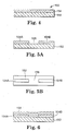
inkjet printhead 150 incorporating the present invention. Figure 5B is an enlarged, plan view illustrating a portion ofinkjet printhead 150 incorporating the present invention. As shown in Figure 4,insulative dielectric 152 is fabricated through any known means, such as a plasma enhanced chemical vapor deposition (PECVD) or a thermal oxide process.Conductive material layer 154 is fabricated on top ofinsulative dielectric 152. In one embodiment,conductive material layer 154 is a resistive layer formed through a physical vapor deposition (PVD) from aluminum and copper. More specifically, in one embodiment,conductive material layer 154 includes up to approximately 10 percent copper in aluminum, preferably up to approximately 2 percent copper in aluminum. Utilizing a small percent of copper in aluminum limits electromigration between adjacent thin film layers. In another preferred embodiment,conductive material layer 154 is formed from titanium or tungsten. A photo imagable masking material such as a photoresist mask is deposited on portions ofconductive material layer 154, thereby exposing other portions ofconductive layer 154. The exposed portions ofconductive layer 154 is removed through a dry etch process known in the art. The photoresist mask is then removed, thereby exposing substantially rectangular-shapedconductors -
Conductors conductors insulative dielectric 152 is fabricated from silicon dioxide. - As shown in Figure 5B,
conductors chamber area 156 betweenconductors Chamber area 156 has a maximum width equal to the distance betweenconductors - Figures 6-9A are enlarged, cross-sectional, partial views illustrating various layers and fabricating steps for
inkjet printhead 150. As shown in Figure 6,dielectric material 158 is deposited ontoinsulative dielectric 152 inchamber 156 and ontoconductors dielectric material 158 fillschamber area 156. The top surface ofdielectric material 158 is then planarized such that the top surface ofdielectric material 158 is level (shown in Figure 7). - In one preferred embodiment, the top surface of
dielectric material 158 is planarized through use of a resistive-etch-back (REB) process. In another embodiment, the top surface ofdielectric material layer 158 is planarized through use of a chemical/mechanical polish (CMP) process. - In one preferred embodiment,
dielectric material 158 is formed from an oxide. More specifically,dielectric material 158 is formed from tetraethylorthosilicate (TEOS) oxide. TEOS oxide provides adequate step coverage, thereby fillingchamber area 156 without voids or gaps. In another preferred embodiment,dielectric material 158 is formed from a silicon-containing material or glass. In yet another preferred embodiment,dielectric material 158 has a thickness in the range of approximately 2,000 to 10,000 angstroms aboveconductors insulative dielectric 152 withinchamber area 156. - As shown in Figures 9A and 9B, vias 160A and 160B are formed through
dielectric material 158, thereby exposing a portion ofconductors dielectric material 158 into three distinct sections, 158A, 158B, and 158C. Whilesections dielectric material 158 are located aboveconductors section 158B ofdielectric material 158 is positioned abovechamber area 156. - Preferable, the present invention utilizes a dry etch procedure in order to define
vias vias vias vias - In another embodiment, vias 160A and 160B can be subdivided into multiple vias having various dielectric barrier walls providing the structure. Thus, if corrosion occurs within a subdivided portion of
vias conductors - In order to produced the desired profile shown in Figure 9C for
vias dielectric material 158 is planarized such that it has a level top surface, as shown in Figure 7.Photoresist mask 162 is then deposited and defined through standard photolithography techniques, as shown in Figure 8.Photoresist mask 162 is subject to a high temperature bake process, thereby creating sloped or concave portions of 162A and162B photoresist mask 162 such that portions ofdielectric material 158 are exposed. The exposed portions ofdielectric material 158 are then etched through a dry etch process, thereby creatingvias vias photoresist mask 162 is removed. - In one preferred embodiment,
photoresist mask 162 is baked at a relatively high temperature, such as greater than 110° Celsius, in order to create sloped or concave portions of 162A and 162B ofphotoresist mask 162. Preferably,photoresist mask 162 is baked at a temperature of 130° Celsius. Sincephotoresist mask 162 is a polymer, the polymer flows and produces a curved or sloped profile or concave section immediately above the desired location ofvias photoresist layer 162 can be controlled through the baking process (i.e., length of time and temperature). - In another embodiment, vias 160A and 160B having sloped walls are formed through a photoresist mask which is deposited and defined, and a dry etch process which changes the selectivity of etch rate between
photoresist mask 162 anddielectric material 158 resulting in a sloped profile as is known in the art. In yet another embodiment, the vias having sloped walls can be formed through a photoresist mask and a wet etch process as is known in the art. - Figures 10A and 10B illustrate
resistive element 164 fabricated withinvias chamber area 156 betweenvias resistive element 164 comes in direct contact withconductors vias conductors resistive element 164 and circuitry external toinkjet printhead 150.Resistive element 164 is fabricated as shown in Figure 10 via conventional means, such as a physical vapor deposition. A photoresist mask covers portions of a resistive material layer to define the shape ofresistive element 164. Definingresistive element 164 through a single photoresist mask and a single etch is an advantage over the prior art because it provides increased dimensional control ofresistive element 164. As shown in Figure 10A,resistive element 164 is fabricated withinvias dielectric material 158 betweenvias resistive element 164 has a thickness in the range of approximately 250 to 1000 angstroms. The sloped walls ofdielectric material 158A permit adequate step coverage. Ifvias - As shown in Figure 10B,
resistive element 164 has a width W. However, it is understood thatresistive element 164 may be fabricated having any one of a variety of configurations, shapes, or sizes, such as a thin trace or a wide trace betweenvias resistive element 164 is that it encloses vias 160A and 160B to ensure a proper electrical connection toconductors resistive element 164 is equal to or greater than the distance between the outer most edges ofvias resistive element 164 which conducts heat to a droplet of ink positioned aboveresistive element 164 corresponds to the distance between the outermost edges ofvias - Figure 11 is an enlarged, cross-sectional, partial view illustrating an alternate embodiment of the present invention. As shown in Figure 11, fill or
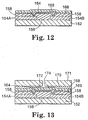
planarization element 166 is fabricated in bothvias resistive element 164 and planarized. In one embodiment, fillelement 166 is formed from a conductive material, such as tungsten. In another embodiment, fillelement 166 is formed from a dielectric material. The addition offill element 66 minimizes the issue of step coverage for passivation layer 168 (shown in Figures 12 and 13). - Figure 12 is an enlarged, cross-sectional view illustrating additional layers and steps of the present invention. As shown in Figure 12,
passivation layer 168 is fabricated on top ofresistive material layer 164 anddielectric material 158.Passivation layer 168 can be formed incorporating various compositions as long as it acts as an insulator layer and/or a protective layer. In one embodiment,passivation layer 168 can be an intermetal dielectric. In another embodiment,passivation layer 168 is a silicon-containing layer, while in yet another embodiment,passivation layer 168 is a dielectric layer. It is desirous to utilize athin passivation layer 168 in order to promote efficiency ofinkjet printhead 150. Therefore, in one preferred embodiment,passivation layer 168 has a thickness of less than approximately 5,000 angstroms aboveresistive material layer 164 betweenvias -
Cavitation layer 169 is fabricated on top ofpassivation layer 168.Cavitation layer 169, which coverspassivation layer 168 andresistive material layer 164, eliminates or minimizes mechanical damage to various elements of the overall structure due to the momentum of collapsing an ink bubble. In one preferred embodiment,cavitation layer 169 comprises tantalum, although other materials, such as, for example, tungsten, may be used. - Figure 13 is an enlarged, cross-sectional view illustrating completed
inkjet printhead 150. As shown in Figure 13,ink barrier layer 170 is fabricated on top ofcavitation layer 169 as is known in the art.Ink barrier layer 170 is fabricated such that firingchamber 172 is developed directly above and in alignment withresistive element 164 betweenvias - In operation, a droplet of ink is positioned within
chamber 172. Electrical current is supplied toresistive element 164 viaconductors resistive element 164 rapidly generates energy in the form of heat. The heat fromresistive element 164 is transferred to a droplet of ink withinchamber 172 until the droplet of ink is "fired" throughnozzle 174. This process is repeated several times in order to produce a desired result. - The present invention provides numerous advantages over the prior art. First, the resistor length of the present invention is defined by the placement of
vias - Second, the resistor structure of the present invention includes a completely flat top surface and does not have the step contour associated with prior art fabrication designs. A flat structure provides consistent bubble nucleation, better scavenging of the firing chamber, and a flatter topology, thereby improving the adhesion and lamination of the barrier structure to the thin film. Third, due to the flat topology of the present structure, the barrier structure is allowed to cover the edge of the resistor. By introducing heat into the floor of the entire firing chamber, ink droplet ejection efficiency is improved.
- Fourth, the present invention utilizes a single mask and a single etch to fabricate a resistive element, rather than using both a dry and a wet etch process as is known in the art.
Vias resistive element 164 andpassivation layer 168. - Although specific embodiments have been illustrated and described herein for purposes of description of the preferred embodiment, it will be appreciated by those of ordinary skill in the art that a wide variety of alternate and/or equivalent implementations calculated to achieve the same purposes may be substituted for the specific embodiments shown and described without departing from the scope of the present invention. Those with skill in the chemical, mechanical, electro-mechanical, electrical, and computer arts will readily appreciate that the present invention may be implemented in a very wide variety of embodiments. This application is intended to cover any adaptations or variations of the preferred embodiments discussed herein. Therefore, it is manifestly intended that this invention be limited only by the claims and the equivalents thereof.
Claims (10)
- A method of fabricating an inkjet printhead (150), the method comprising:depositing a conducting material layer (154) onto an insulative dielectric (152);removing a portion of the conducting material layer to expose the insulative dielectric, thereby forming a chamber (156) between first and second conductors (154A, 154B);depositing a dielectric material (158) onto the first and second conductors and onto the insulative dielectric in the chamber;etching a first via (160A) through the dielectric material to expose a portion of the first conductor such that side walls of the first via are sloped;etching a second via (160B) through the dielectric material to expose a portion of the second conductor such that side walls of the second via are sloped;fabricating a resistive material layer (164) within the first and second vias and on the dielectric material between the first and second vias; anddepositing a passivation material layer (168) onto the dielectric material and the resistive material layer.
- The method of claim 1, wherein the steps of etching the first and second vias through the dielectric material further comprises:depositing and developing a photoresist mask (162) on to the dielectric material;selectively heating exposed sections of the photoresist mask to create first and second concave sections of the photoresist mask, thereby exposing portions of the dielectric material; anddry etching the exposed portions of the dielectric material, thereby creating the first and second vias in the dielectric material having sloped walls.
- The method of claim 1, wherein the steps of etching the first and second vias through the dielectric material further comprises:depositing and developing a photoresist mask onto the dielectric, thereby defining exposed portions of the dielectric material; anddry etching the exposed portions of the dielectric material, thereby creating the first and second vias in the dielectric material having sloped walls.
- The method of claim 1, wherein the steps of etching the first and second vias through the dielectric material further comprises:depositing and developing a photoresist mask onto the dielectric, thereby defining exposed portions of the dielectric material; andwet etching exposed portions of the dielectric material, thereby creating the first and second vias in the dielectric material having sloped walls.
- The method of claim 1, and further comprising:depositing a photoresist mask on to a portion of the resistive material layer corresponding to a resistor element (164);dry etching an exposed portion of the resistive material layer; andremoving the photoresist mask, thereby exposing the resistive element having a length at least as long as a distance between an outer edge of the first and second vias in the dielectric material.
- An inkjet printhead (150) comprising:an insulative dielectric (152);first and second conductors (154A, 154B) fabricated on the insulative dielectric, the first and second conductors having a chamber (156) formed therebetween, the first and second conductors each having a width (W);a dielectric material (158) fabricated on the first and second conductors and on the insulative dielectric in the chamber;a first via (160A) formed in the dielectric material to expose a portion of the first conductor, the first via having sloped side walls;a second via (160B) formed in the dielectric material to expose a portion of the second conductor, the second via having sloped side walls;a resistive material layer (164) formed within the first and second vias and on the dielectric material between the first and second vias, the resistive material layer having a length (L) at least as long as a distance between the first and second vias in the dielectric material;a passivation material layer (168) formed onto the dielectric material and onto the resistive material layer.
- The inkjet printhead apparatus of claim 6, wherein the first and second vias each have sloped walls sloped at an angle in the range of approximately 10-60 degrees.
- The inkjet printhead of claim 6, wherein the first and second conductors include up to approximately 2 percent copper in aluminum.
- The inkjet printhead of claim 6, wherein the dielectric material is fabricated from tetraethylorthosilicate (TEOS) oxide.
- The inkjet printhead of claim 60, and further comprising:an ink barrier layer (170) having a chamber (172) formed therein between the first and second vias, the chamber located above the resistive layer between the first and second vias.
Applications Claiming Priority (2)
| Application Number | Priority Date | Filing Date | Title |
|---|---|---|---|
| US09/611,810 US6481831B1 (en) | 2000-07-07 | 2000-07-07 | Fluid ejection device and method of fabricating |
| US611810 | 2000-07-07 |
Publications (3)
| Publication Number | Publication Date |
|---|---|
| EP1170129A2 true EP1170129A2 (en) | 2002-01-09 |
| EP1170129A3 EP1170129A3 (en) | 2002-01-30 |
| EP1170129B1 EP1170129B1 (en) | 2005-10-12 |
Family
ID=24450490
Family Applications (1)
| Application Number | Title | Priority Date | Filing Date |
|---|---|---|---|
| EP01305328A Expired - Lifetime EP1170129B1 (en) | 2000-07-07 | 2001-06-19 | Inkjet printhead and method of fabricating an inkjet printhead |
Country Status (4)
| Country | Link |
|---|---|
| US (1) | US6481831B1 (en) |
| EP (1) | EP1170129B1 (en) |
| JP (1) | JP2002079679A (en) |
| DE (1) | DE60113926T2 (en) |
Cited By (4)
| Publication number | Priority date | Publication date | Assignee | Title |
|---|---|---|---|---|
| WO2005102709A1 (en) * | 2004-04-23 | 2005-11-03 | Hewlett-Packard Development Company, L.P. | Inkjet print cartridge |
| EP2017083A1 (en) * | 2007-07-16 | 2009-01-21 | Samsung Electronics Co., Ltd. | Inkjet Print Head and Manufacturing Method Thereof |
| WO2015116050A1 (en) * | 2014-01-29 | 2015-08-06 | Hewlett-Packard Development Company, L.P. | Thermal ink jet printhead |
| EP3555925A4 (en) * | 2016-12-15 | 2020-11-18 | Griffith University | Silicon carbide schottky diodes |
Families Citing this family (14)
| Publication number | Priority date | Publication date | Assignee | Title |
|---|---|---|---|---|
| US7083265B2 (en) * | 2001-10-31 | 2006-08-01 | Hewlett-Packard Development Company, L.P. | Circuit routing for printhead having increased corrosion resistance |
| JP3812485B2 (en) * | 2002-04-10 | 2006-08-23 | ソニー株式会社 | Liquid ejection apparatus and printer |
| JP2005067164A (en) * | 2003-08-28 | 2005-03-17 | Sony Corp | Liquid ejection head, liquid ejector, and process for manufacturing liquid ejection head |
| KR100517515B1 (en) * | 2004-01-20 | 2005-09-28 | 삼성전자주식회사 | Method for manufacturing monolithic inkjet printhead |
| US7239006B2 (en) * | 2004-04-14 | 2007-07-03 | International Business Machines Corporation | Resistor tuning |
| US7293359B2 (en) * | 2004-04-29 | 2007-11-13 | Hewlett-Packard Development Company, L.P. | Method for manufacturing a fluid ejection device |
| US7387370B2 (en) * | 2004-04-29 | 2008-06-17 | Hewlett-Packard Development Company, L.P. | Microfluidic architecture |
| US20080147495A1 (en) * | 2006-12-19 | 2008-06-19 | General Electric Company | System and method for providing promotions |
| US20080147496A1 (en) * | 2006-12-19 | 2008-06-19 | General Electric Company | System and method for providing promotions |
| US7862156B2 (en) * | 2007-07-26 | 2011-01-04 | Hewlett-Packard Development Company, L.P. | Heating element |
| US7837886B2 (en) * | 2007-07-26 | 2010-11-23 | Hewlett-Packard Development Company, L.P. | Heating element |
| US8336981B2 (en) * | 2009-10-08 | 2012-12-25 | Hewlett-Packard Development Company, L.P. | Determining a healthy fluid ejection nozzle |
| US20120091121A1 (en) * | 2010-10-19 | 2012-04-19 | Zachary Justin Reitmeier | Heater stack for inkjet printheads |
| US20180102318A1 (en) * | 2016-10-12 | 2018-04-12 | Globalfoundries Inc. | Compound resistor structure for semiconductor device |
Citations (3)
| Publication number | Priority date | Publication date | Assignee | Title |
|---|---|---|---|---|
| EP0603821A2 (en) * | 1992-12-22 | 1994-06-29 | Canon Kabushiki Kaisha | Ink-jet printhead, production method thereof and printing apparatus with the ink-jet printhead |
| EP0674995A2 (en) * | 1994-03-29 | 1995-10-04 | Canon Kabushiki Kaisha | Substrate for ink jet head, ink jet head, ink jet pen, and ink jet apparatus |
| US6079811A (en) * | 1997-01-24 | 2000-06-27 | Lexmark International, Inc. | Ink jet printhead having a unitary actuator with a plurality of active sections |
Family Cites Families (15)
| Publication number | Priority date | Publication date | Assignee | Title |
|---|---|---|---|---|
| US4513298A (en) | 1983-05-25 | 1985-04-23 | Hewlett-Packard Company | Thermal ink jet printhead |
| US4535343A (en) | 1983-10-31 | 1985-08-13 | Hewlett-Packard Company | Thermal ink jet printhead with self-passivating elements |
| US4602421A (en) | 1985-04-24 | 1986-07-29 | The United States Of America As Represented By The Secretary Of The Air Force | Low noise polycrystalline semiconductor resistors by hydrogen passivation |
| US4862197A (en) | 1986-08-28 | 1989-08-29 | Hewlett-Packard Co. | Process for manufacturing thermal ink jet printhead and integrated circuit (IC) structures produced thereby |
| US5364743A (en) * | 1990-12-21 | 1994-11-15 | Xerox Corporation | Process for fabrication of bubble jet using positive resist image reversal for lift off of passivation layer |
| US5075250A (en) * | 1991-01-02 | 1991-12-24 | Xerox Corporation | Method of fabricating a monolithic integrated circuit chip for a thermal ink jet printhead |
| US5159353A (en) | 1991-07-02 | 1992-10-27 | Hewlett-Packard Company | Thermal inkjet printhead structure and method for making the same |
| US5232865A (en) | 1991-07-24 | 1993-08-03 | Micron Technology, Inc. | Method of fabricating vertically integrated oxygen-implanted polysilicon resistor |
| US5159430A (en) | 1991-07-24 | 1992-10-27 | Micron Technology, Inc. | Vertically integrated oxygen-implanted polysilicon resistor |
| JP2750992B2 (en) | 1992-08-12 | 1998-05-18 | 三菱電機株式会社 | Semiconductor device and manufacturing method thereof |
| US5330930A (en) | 1992-12-31 | 1994-07-19 | Chartered Semiconductor Manufacturing Pte Ltd. | Formation of vertical polysilicon resistor having a nitride sidewall for small static RAM cell |
| US6008082A (en) | 1995-09-14 | 1999-12-28 | Micron Technology, Inc. | Method of making a resistor, method of making a diode, and SRAM circuitry and other integrated circuitry |
| US5883650A (en) | 1995-12-06 | 1999-03-16 | Hewlett-Packard Company | Thin-film printhead device for an ink-jet printer |
| US5683930A (en) | 1995-12-06 | 1997-11-04 | Micron Technology Inc. | SRAM cell employing substantially vertically elongated pull-up resistors and methods of making, and resistor constructions and methods of making |
| US5710070A (en) | 1996-11-08 | 1998-01-20 | Chartered Semiconductor Manufacturing Pte Ltd. | Application of titanium nitride and tungsten nitride thin film resistor for thermal ink jet technology |
-
2000
- 2000-07-07 US US09/611,810 patent/US6481831B1/en not_active Expired - Fee Related
-
2001
- 2001-06-19 EP EP01305328A patent/EP1170129B1/en not_active Expired - Lifetime
- 2001-06-19 DE DE60113926T patent/DE60113926T2/en not_active Expired - Lifetime
- 2001-07-06 JP JP2001205523A patent/JP2002079679A/en active Pending
Patent Citations (3)
| Publication number | Priority date | Publication date | Assignee | Title |
|---|---|---|---|---|
| EP0603821A2 (en) * | 1992-12-22 | 1994-06-29 | Canon Kabushiki Kaisha | Ink-jet printhead, production method thereof and printing apparatus with the ink-jet printhead |
| EP0674995A2 (en) * | 1994-03-29 | 1995-10-04 | Canon Kabushiki Kaisha | Substrate for ink jet head, ink jet head, ink jet pen, and ink jet apparatus |
| US6079811A (en) * | 1997-01-24 | 2000-06-27 | Lexmark International, Inc. | Ink jet printhead having a unitary actuator with a plurality of active sections |
Cited By (7)
| Publication number | Priority date | Publication date | Assignee | Title |
|---|---|---|---|---|
| WO2005102709A1 (en) * | 2004-04-23 | 2005-11-03 | Hewlett-Packard Development Company, L.P. | Inkjet print cartridge |
| US7832839B2 (en) | 2004-04-23 | 2010-11-16 | Hewlett-Packard Development Company, L.P. | Inkjet print cartridge |
| EP2017083A1 (en) * | 2007-07-16 | 2009-01-21 | Samsung Electronics Co., Ltd. | Inkjet Print Head and Manufacturing Method Thereof |
| WO2015116050A1 (en) * | 2014-01-29 | 2015-08-06 | Hewlett-Packard Development Company, L.P. | Thermal ink jet printhead |
| US9776402B2 (en) | 2014-01-29 | 2017-10-03 | Hewlett-Packard Development Company, L.P. | Thermal ink jet printhead |
| EP3555925A4 (en) * | 2016-12-15 | 2020-11-18 | Griffith University | Silicon carbide schottky diodes |
| US10971580B2 (en) | 2016-12-15 | 2021-04-06 | Griffith University | Silicon carbide schottky diodes with tapered negative charge density |
Also Published As
| Publication number | Publication date |
|---|---|
| EP1170129A3 (en) | 2002-01-30 |
| US6481831B1 (en) | 2002-11-19 |
| JP2002079679A (en) | 2002-03-19 |
| DE60113926D1 (en) | 2006-02-23 |
| EP1170129B1 (en) | 2005-10-12 |
| DE60113926T2 (en) | 2006-07-20 |
Similar Documents
| Publication | Publication Date | Title |
|---|---|---|
| EP1170129B1 (en) | Inkjet printhead and method of fabricating an inkjet printhead | |
| US6457814B1 (en) | Fluid-jet printhead and method of fabricating a fluid-jet printhead | |
| JP3388240B2 (en) | INK JET PRINT HEAD AND ITS MANUFACTURING METHOD | |
| US7169539B2 (en) | Monolithic ink-jet printhead having a tapered nozzle and method for manufacturing the same | |
| JP2005219500A (en) | Heating element, fluid heating device, inkjet printhead and print cartridge having it and manufacturing method therefor | |
| KR100408268B1 (en) | Bubble-jet type ink-jet printhead and manufacturing method thereof | |
| US6457815B1 (en) | Fluid-jet printhead and method of fabricating a fluid-jet printhead | |
| US7452058B2 (en) | Substantially planar ejection actuators and methods relating thereto | |
| KR100477707B1 (en) | Method of manufacturing Monolithic inkjet printhead | |
| KR100421027B1 (en) | Inkjet printhead and manufacturing method thereof | |
| KR20040055230A (en) | Inkjet printhead and manufacturing method thereof | |
| KR100497389B1 (en) | Inkjet printhead and method of manufacturing thereof | |
| KR100477704B1 (en) | Monolithic inkjet printhead and method of manufacturing thereof | |
| JP2005047270A (en) | Ink jet printing head and its manufacturing method | |
| KR100513717B1 (en) | Bubble-jet type inkjet printhead | |
| KR100503086B1 (en) | Monolithic inkjet printhead and method of manufacturing thereof | |
| KR100484202B1 (en) | Inkjet printhead with reverse heater and method of manufacturing thereof |
Legal Events
| Date | Code | Title | Description |
|---|---|---|---|
| PUAI | Public reference made under article 153(3) epc to a published international application that has entered the european phase |
Free format text: ORIGINAL CODE: 0009012 |
|
| PUAL | Search report despatched |
Free format text: ORIGINAL CODE: 0009013 |
|
| AK | Designated contracting states |
Kind code of ref document: A2 Designated state(s): AT BE CH CY DE DK ES FI FR GB GR IE IT LI LU MC NL PT SE TR Kind code of ref document: A2 Designated state(s): DE FR GB |
|
| AX | Request for extension of the european patent |
Free format text: AL;LT;LV;MK;RO;SI |
|
| AK | Designated contracting states |
Kind code of ref document: A3 Designated state(s): AT BE CH CY DE DK ES FI FR GB GR IE IT LI LU MC NL PT SE TR |
|
| AX | Request for extension of the european patent |
Free format text: AL;LT;LV;MK;RO;SI |
|
| 17P | Request for examination filed |
Effective date: 20020321 |
|
| AKX | Designation fees paid |
Free format text: DE FR GB |
|
| 17Q | First examination report despatched |
Effective date: 20040614 |
|
| GRAP | Despatch of communication of intention to grant a patent |
Free format text: ORIGINAL CODE: EPIDOSNIGR1 |
|
| GRAS | Grant fee paid |
Free format text: ORIGINAL CODE: EPIDOSNIGR3 |
|
| GRAA | (expected) grant |
Free format text: ORIGINAL CODE: 0009210 |
|
| AK | Designated contracting states |
Kind code of ref document: B1 Designated state(s): DE FR GB |
|
| REG | Reference to a national code |
Ref country code: GB Ref legal event code: FG4D |
|
| REF | Corresponds to: |
Ref document number: 60113926 Country of ref document: DE Date of ref document: 20060223 Kind code of ref document: P |
|
| ET | Fr: translation filed | ||
| PLBE | No opposition filed within time limit |
Free format text: ORIGINAL CODE: 0009261 |
|
| STAA | Information on the status of an ep patent application or granted ep patent |
Free format text: STATUS: NO OPPOSITION FILED WITHIN TIME LIMIT |
|
| 26N | No opposition filed |
Effective date: 20060713 |
|
| REG | Reference to a national code |
Ref country code: GB Ref legal event code: 732E Free format text: REGISTERED BETWEEN 20120329 AND 20120404 |
|
| PGFP | Annual fee paid to national office [announced via postgrant information from national office to epo] |
Ref country code: DE Payment date: 20130523 Year of fee payment: 13 Ref country code: GB Payment date: 20130527 Year of fee payment: 13 |
|
| PGFP | Annual fee paid to national office [announced via postgrant information from national office to epo] |
Ref country code: FR Payment date: 20130724 Year of fee payment: 13 |
|
| REG | Reference to a national code |
Ref country code: DE Ref legal event code: R119 Ref document number: 60113926 Country of ref document: DE |
|
| GBPC | Gb: european patent ceased through non-payment of renewal fee |
Effective date: 20140619 |
|
| REG | Reference to a national code |
Ref country code: DE Ref legal event code: R119 Ref document number: 60113926 Country of ref document: DE Effective date: 20150101 |
|
| REG | Reference to a national code |
Ref country code: FR Ref legal event code: ST Effective date: 20150227 |
|
| PG25 | Lapsed in a contracting state [announced via postgrant information from national office to epo] |
Ref country code: DE Free format text: LAPSE BECAUSE OF NON-PAYMENT OF DUE FEES Effective date: 20150101 |
|
| PG25 | Lapsed in a contracting state [announced via postgrant information from national office to epo] |
Ref country code: GB Free format text: LAPSE BECAUSE OF NON-PAYMENT OF DUE FEES Effective date: 20140619 Ref country code: FR Free format text: LAPSE BECAUSE OF NON-PAYMENT OF DUE FEES Effective date: 20140630 |