EP1168619A1 - Boosted switch device for a sampler of an analogue/digital converter, and operating method thereof - Google Patents
Boosted switch device for a sampler of an analogue/digital converter, and operating method thereof Download PDFInfo
- Publication number
- EP1168619A1 EP1168619A1 EP00830430A EP00830430A EP1168619A1 EP 1168619 A1 EP1168619 A1 EP 1168619A1 EP 00830430 A EP00830430 A EP 00830430A EP 00830430 A EP00830430 A EP 00830430A EP 1168619 A1 EP1168619 A1 EP 1168619A1
- Authority
- EP
- European Patent Office
- Prior art keywords
- terminal
- switch device
- switch
- charge storage
- control signal
- Prior art date
- Legal status (The legal status is an assumption and is not a legal conclusion. Google has not performed a legal analysis and makes no representation as to the accuracy of the status listed.)
- Withdrawn
Links
- 238000011017 operating method Methods 0.000 title claims description 5
- 239000003990 capacitor Substances 0.000 claims abstract description 26
- 238000000034 method Methods 0.000 claims description 7
- 238000005070 sampling Methods 0.000 description 9
- 238000006243 chemical reaction Methods 0.000 description 5
- 238000010586 diagram Methods 0.000 description 5
- 230000000694 effects Effects 0.000 description 5
- 230000003111 delayed effect Effects 0.000 description 2
- 238000011161 development Methods 0.000 description 2
- 230000018109 developmental process Effects 0.000 description 2
- 229910052710 silicon Inorganic materials 0.000 description 2
- 239000010703 silicon Substances 0.000 description 2
- 230000002123 temporal effect Effects 0.000 description 2
- 239000002699 waste material Substances 0.000 description 2
- 239000008186 active pharmaceutical agent Substances 0.000 description 1
- 238000013461 design Methods 0.000 description 1
- 238000004519 manufacturing process Methods 0.000 description 1
- 238000012986 modification Methods 0.000 description 1
- 230000004048 modification Effects 0.000 description 1
- 230000001681 protective effect Effects 0.000 description 1
Images

Classifications
-
- H—ELECTRICITY
- H03—ELECTRONIC CIRCUITRY
- H03K—PULSE TECHNIQUE
- H03K17/00—Electronic switching or gating, i.e. not by contact-making and –breaking
- H03K17/16—Modifications for eliminating interference voltages or currents
- H03K17/161—Modifications for eliminating interference voltages or currents in field-effect transistor switches
- H03K17/165—Modifications for eliminating interference voltages or currents in field-effect transistor switches by feedback from the output circuit to the control circuit
-
- G—PHYSICS
- G11—INFORMATION STORAGE
- G11C—STATIC STORES
- G11C27/00—Electric analogue stores, e.g. for storing instantaneous values
- G11C27/02—Sample-and-hold arrangements
-
- H—ELECTRICITY
- H03—ELECTRONIC CIRCUITRY
- H03K—PULSE TECHNIQUE
- H03K17/00—Electronic switching or gating, i.e. not by contact-making and –breaking
- H03K17/06—Modifications for ensuring a fully conducting state
- H03K17/063—Modifications for ensuring a fully conducting state in field-effect transistor switches
Definitions
- the present invention relates to a boosted switch device for a sampler of an analogue/digital converter, and to an operating method thereof.
- analogue/digital conversion systems can be subdivided into two main categories, according to the conversion principle on the basis of which they operate: the first category includes the so-called Nyquist analogue/digital conversion systems, i.e.
- the second category includes the so-called over-sampling analogue/digital conversion systems, which can be schematised with a continuous-time anti-aliasing filter, an over-sampling analogue/digital converter, and a digital channel filter which are connected to one another in cascade.
- both categories carry out the conversion of an analogue signal, i.e. of a signal which is continuous in time and in amplitude, into a sampled data signal, i.e. which is continuous in time and discrete in amplitude, by means of a so-called sampler.
- FIG 1 shows the general circuit diagram of the sampler which is best known and most commonly used in the applications.
- the sampler indicated as a whole by 1, comprises an input terminal 2, at which there is present an input voltage V A to be sampled; an output terminal 4; a sampling capacitor 6 connected between a first and a second node 8, 10; a first switch device 12 controlled by a first control signal F1D, and connected between the input terminal 2 of the sampler 1 and the first node 8; a second switch device 14 controlled by a second control signal F2D, and connected between the first node 8 and a ground line 16 set to a ground potential V GND , typically 0 V; a third switch device 18 controlled by a third control signal F1, and connected between the second node 10 and the ground line 16; and a fourth switch device 20 controlled by a fourth control signal F2, and connected between the output terminal 4 of the sampler 1, and the second node 10.
- the output terminal 4 of the sampler is then typically connected to the virtual ground of an operational amplifier (not shown), with which it forms a switched-capacitor integrator.
- figure 2 shows the temporal development of the four control signals F1, F2, F1D, F2D, which are commonly also known as “phases", and are supplied to the switch devices 12, 14, 18, 20 of the sampler 1.
- the first and the second control signals F1D and F2D are exact replicas respectively of the third and fourth control signals, which are temporally delayed compared with the latter, by a delay T R of approximately a few nanoseconds.
- the first and second control signals F1D and F2D do not overlap one another temporally, in other words the first and second control signals F1D and F2D never assume the same logic level simultaneously, just as the third and fourth control signals F1 and F2 do not overlap one another temporally.
- neither the first and fourth control signals F1D, F2, nor the second and third control signals F2D, F1 overlap one another temporally.
- sampler 1 The operation of the sampler 1 is known, and will thus be described here briefly and only to the extent necessary for understanding of the problem on which the present invention is based.
- the sampler capacitor 6 is connected cyclically and in an alternating manner between the input terminal 2 and the ground line 16, and between the latter and the output terminal 4.
- the first and the fourth control signals F1, F1D assume a high logic level
- the input voltage V A is sampled, and the sample is stored in the sampler capacitor 6
- the second and the third control signal F2, F2D assume a high logic level
- the sample of the input voltage V A which is stored in the sampler capacitor 6 is transferred to the output terminal 4 of the sampler 1, and consequently to the virtual ground of the operational amplifier, with which it forms the aforementioned switched-capacitor integrator.
- the prior art samplers had the disadvantage that they introduced onto the output signal V B unacceptable distortions, generated mainly by the switch devices 12, 14, 18, 20.
- these switch devices are not ideal, but have capacitances, and thus associated charges, which vary strongly according to the input voltage V A , at the instant at which these switch devices open, they introduce onto the output signal V B distortions which detract considerably from the performance of the sampler.
- the distortion of the output signal V B is strongly reduced, for input frequencies lower than 10 kHz, i.e. for harmonics of the input voltage V A with frequencies lower than 10 kHz.
- the first switch device 12 was usually formed by a CMOS transfer-gate switch having the circuit structure shown in figure 3, i.e. formed by an NMOS transistor 22 and by a PMOS transistor 24 having drain terminals connected to one another and to the input terminal 2 of the sampler 1, source terminals connected to one another and to the first node 8, and gate terminals receiving respectively the first control signal F1D and the first negated control signal F1D ⁇ , the latter being generated by means of a logic inverter (not shown).
- a CMOS transfer-gate switch having the circuit structure shown in figure 3, i.e. formed by an NMOS transistor 22 and by a PMOS transistor 24 having drain terminals connected to one another and to the input terminal 2 of the sampler 1, source terminals connected to one another and to the first node 8, and gate terminals receiving respectively the first control signal F1D and the first negated control signal F1D ⁇ , the latter being generated by means of a logic inverter (not shown).
- the switch devices with the circuit structure shown in figure 3 have series resistance which varies considerably according to the input voltage V A , thus causing strong distortions at a high frequency.
- a switch device having the circuit structure shown in figure 4 is proposed, which, for the reasons given hereinafter, is commonly known as "bootstrapped clock-boosted switch".
- the switch device comprises an NMOS transistor 30 having a drain terminal connected to the input terminal 2 of the sampler 1, a source terminal connected to the first node 8 of the sampler 1, and a gate terminal connected to a third node 32; a PMOS transistor 34 having a drain terminal connected to the third node 32, source and bulk terminals connected to one another and to a fourth node 36, and a gate terminal receiving the first negated control signal F1D ⁇ ; and an NMOS transistor 38 having a drain terminal connected to the third node 32, a source terminal connected to the ground line 16, and a gate terminal receiving the second control signal F2D.
- the switch device 12' further comprises an amplifier 40, and a CMOS transfer-gate switch 42, which are connected to one another in series between the input terminal 2 and the fourth node 36.
- the amplifier 40 has a unit gain
- the CMOS transfer-gate switch 42 is formed by an NMOS transistor 44 and a PMOS transistor 46, having drain terminals connected to one another and to the output terminal of the amplifier 40, source terminals connected to one another and to the fourth node 36, and gate terminals receiving respectively the second control signal F2D and the second negated control signal F2D ⁇ , the latter being generated by means of a logic inverter (not shown).
- the switch device 12' further comprises a so-called bootstrap capacitor 48 connected between the fourth node 36 and a fifth node 50; a PMOS transistor 52 having a drain terminal connected to the fifth node 50, a source terminal connected to a supply line 54 set to a supply potential V CC , typically approximately 3 V, and a gate terminal receiving the first negated control signal F1D ⁇ ; and an NMOS transistor 56 having a drain terminal connected to the fifth node 50, a source terminal connected to the ground line 16, and a gate terminal receiving the second control signal F2D.
- the NMOS transistor 30 acts as a switch, and is on when the first control signal F1D is in the high logic state, and is off when the first control signal F1D is in the low logic state, whereas the bootstrap capacitor 48 acts as a floating battery.
- the control signal F2D When the control signal F2D is in the high logic state, and therefore, owing to the non-overlapping condition, the first control signal F1D is in the low logic state, the NMOS transistors 38 and 56 are on, the CMOS switch 42 is closed, and the PMOS transistors 34 and 52 are off.
- the third node 32 is connected to the ground line 16, and therefore keeps the NMOS transistor 30 off, whereas the bootstrap capacitor 48 is connected between the output terminal of the amplifier 40, at which the input voltage V A is present, since the amplifier 40 has a unit gain, and the ground line 16, and therefore the input voltage V A is applied to the terminals of the bootstrap capacitor 48.
- the NMOS transistors 38 and 56 are off, the CMOS switch 42 is open, and the PMOS transistors 34 and 52 are on, such that the bootstrap capacitor 48 is connected between the supply line 60 and the gate terminal of the NMOS transistor 64.
- the fifth node 50 is connected to the supply line 54, and therefore to the fourth node 36, and consequently, a voltage equivalent to V CC +V A is present at the gate terminal of the NMOS transistor 30.
- the bootstrap capacitor 48 is connected cyclically and in an alternating manner between the input terminal 2 and the gate terminal of the NMOS transistor 30, and between the latter and the supply line 54.
- the gate-source voltage V GS and the drain-source voltage V DS of the NMOS transistor 30 during conduction are approximately constant, and equivalent to the supply voltage V CC , independently of the input voltage V A (bootstrapping effect of the gate-source voltage) and the potential of the gate terminal of the NMOS transistor 30 exceeds the supply voltage V CC supplied to the switch device 12' (boosting effect of the gate terminal), and hence the name "bootstrapped clock-boosted switch" of the switch device 12'.
- the series resistance R ON of a MOS device during conduction is, in the first approximation, inversely proportional to the difference between the gate-source voltage V GS and the threshold voltage V TH of the MOS device, if the gate-source voltage V GS is independent from the input voltage V A , the sole cause of distortion is that which is associated with dependence of the threshold voltage V TH on the input voltage V A , which is in any case somewhat small.
- a first limitation of the switch device 12' consists in the fact that the input voltage V A must have a bandwidth which is limited to frequencies which are far smaller than the sampling frequency, otherwise the variations in the input voltage V A from one phase to the next, i.e. from the phase in which the first control signal F1D is in the high logic state and the second control signal F2D is in the low logic state, to the opposite phase, in which the first control signal F1D is in the low logic state, and the second control signal F2D is in the high logic state, would be high, the gate-source voltage V GS of the NMOS transistor 30 would not be constant and equivalent to the supply voltage V CC , and therefore all the advantages of the structure described in the aforementioned article would be lost.
- a second limitation of the switch device 12' consists in the fact that when the first control signal F1D is in the high logic state, the third and fourth nodes 32, 36 go to a voltage which is equivalent to V CC +V A , such that problems of reliability could arise if V CC +V A were greater than the maximum operating voltage which can be withstood by integrated devices, which is determined by the technological process used for manufacture of the integrated devices.
- the maximum operating voltage which can be withstood by integrated devices is equivalent to 4.6 V, and if the supply voltage V CC were equivalent to 3.3 V, as is typically required by the user, in order for V CC +V A not to exceed the maximum operating voltage, it is necessary to limit the maximum input voltage V A to 1.3 V, and this leads to a loss of signal/noise ratio of the A/D converter in which the switch device 12' is inserted.
- the aim of the present invention is to provide a boosted switch device and a sampler, which are free from the above-described disadvantages.
- a further object of the present invention is to provide an operating method of a boosted switch device for a sampler, which makes it possible to eliminate the above-described disadvantages.
- a boosted switch device for a sampler of an analogue/digital converter is provided, as defined in claim 1.
- a sampler for an analogue/digital converter is also provided, as defined in claim 9.
- an operating method of a boosted switch device for a sampler of an analogue/digital converter is also provided, as defined in claim 11.
- the switch device 12" comprises a supply line 60 set to a supply potential V CC , typically approximately 3 V; a ground line 62 set to a ground potential V GND , typically 0 V; an NMOS transistor 64 having a drain terminal connected to the input terminal 2 of the sampler 1, a source terminal connected to the node 8 of the sampler 1, and a gate terminal connected to a first node 66; a bootstrap capacitor 68 connected between a second and a third node 70, 72; a PMOS transistor 74 having a drain terminal connected to the first node 66, source and bulk terminals connected to the second node 70, and a gate terminal receiving the first negated control signal F1D ⁇ ; an NMOS transistor 76 having a drain terminal connected to the first node 66, a source terminal connected to the ground line 62, and a gate terminal receiving the second control signal F2D; an NMOS transistor 78 having a drain terminal connected to the supply line 60, a source terminal connected to the second node 70,
- the switch device 12" operates as follows.
- the NMOS transistor 64 acts as a switch, and is on when the first control signal F1D is in the high logic state, and is off when the first control signal F1D is in the low logic state, whereas the bootstrap capacitor 68 acts as a floating battery.
- the control signal F2D When the control signal F2D is in the high logic state, and therefore, owing to the non-overlapping condition, the first control signal F1D is in the low logic state, the NMOS transistors 76, 78 and 80 are on, the CMOS switch 82 is open, and the PMOS transistor 74 is off.
- the first node 66 is connected to the ground line 62, and therefore keeps the NMOS transistor 64 off, whereas the bootstrap capacitor 68 is connected between the supply line 60 and the ground line 62, and therefore the supply voltage V CC is applied to the terminals of the bootstrap capacitor.
- the source terminal of the NMOS transistor 78 can be taken to a voltage which is equivalent at the most to V CC -V TH , such that the bootstrap capacitor 68 is charged to a voltage equivalent to V CC -V TH .
- the NMOS transistors 76, 78 and 80 are off, the CMOS switch 82 is closed, and the PMOS transistor 74 is on, such that the bootstrap capacitor 68 is connected between the input terminal 2 and the gate terminal of the NMOS transistor 64.
- the third node 72 is connected to the input terminal 2, at which the input voltage V A is present, whereas at the second node 70, and therefore at the gate terminal of the NMOS transistor 64, a voltage equivalent to approximately V CC -V TH +V A is present.
- the gate-source voltage V GS and the gate-drain voltage V GD of the NMOS transistor 64 during conduction are approximately constant, and equivalent to V CC -V TH , independently of the input voltage V A (bootstrapping effect of the gate-source voltage) and the potential of the gate terminal of the NMOS transistor 64 exceeds the supply voltage V CC supplied to the switch device 12" (boosting effect of the gate terminal), with the advantages concerning linearisation of the series resistance R ON of the NMS transistor 64 during conduction, previously described for the switch device 12'.
- the bootstrap capacitor 48 is connected cyclically and in an alternating manner between the input terminal 2 and the ground line 16, and between the supply line 54 and the gate terminal of the NMOS transistor 30, in the switch device 12"
- the bootstrap capacitor 68 is connected cyclically and in an alternating manner between the supply line 60 and the ground line 62, and between the input terminal 2 and the gate terminal of the NMOS transistor 64.
- the switch device 12" maintains the advantages of the switch device 12', but does not have the disadvantages of the latter.
- the variations in the input voltage V A are “seen” instantly on the gate terminal of the NMOS transistor 64, such that the gate-source voltage V GS of the NMOS transistor 64 always remains constant, irrespective of the maximum frequency of the input voltage V A , and therefore it is not necessary to limit the bandwidth thereof, such that it is possible to use the Nyquist sampling frequency, with the resulting benefits from the point of view of waste of power and area on the silicon.
- the switch device 12" when the first control signal F1D is in the high logic state, the first and the second nodes 66 and 70 go to a voltage equivalent to V CC -V TH +V A , such that the problems of reliability, which arise only if V CC -V TH +V A is greater than the maximum operating voltage which can be withstood by integrated devices, are greatly reduced.
Landscapes
- Electronic Switches (AREA)
Abstract
Description
- The present invention relates to a boosted switch device for a sampler of an analogue/digital converter, and to an operating method thereof.
- As is known, broadly speaking, analogue/digital conversion systems can be subdivided into two main categories, according to the conversion principle on the basis of which they operate: the first category includes the so-called Nyquist analogue/digital conversion systems, i.e. which can be schematised with a continuous-time anti-aliasing filter, a switched-capacitor channel filter, and a Nyquist analogue/digital converter, which are connected to one another in cascade, whereas the second category includes the so-called over-sampling analogue/digital conversion systems, which can be schematised with a continuous-time anti-aliasing filter, an over-sampling analogue/digital converter, and a digital channel filter which are connected to one another in cascade.
- However, both categories carry out the conversion of an analogue signal, i.e. of a signal which is continuous in time and in amplitude, into a sampled data signal, i.e. which is continuous in time and discrete in amplitude, by means of a so-called sampler.
- Figure 1 shows the general circuit diagram of the sampler which is best known and most commonly used in the applications.
- In particular, as illustrated in figure 1, the sampler, indicated as a whole by 1, comprises an
input terminal 2, at which there is present an input voltage VA to be sampled; an output terminal 4; asampling capacitor 6 connected between a first and asecond node first switch device 12 controlled by a first control signal F1D, and connected between theinput terminal 2 of thesampler 1 and thefirst node 8; asecond switch device 14 controlled by a second control signal F2D, and connected between thefirst node 8 and aground line 16 set to a ground potential VGND, typically 0 V; athird switch device 18 controlled by a third control signal F1, and connected between thesecond node 10 and theground line 16; and afourth switch device 20 controlled by a fourth control signal F2, and connected between the output terminal 4 of thesampler 1, and thesecond node 10. - The output terminal 4 of the sampler is then typically connected to the virtual ground of an operational amplifier (not shown), with which it forms a switched-capacitor integrator.
- On the other hand, figure 2 shows the temporal development of the four control signals F1, F2, F1D, F2D, which are commonly also known as "phases", and are supplied to the
switch devices sampler 1. In particular, it can be noted that the first and the second control signals F1D and F2D are exact replicas respectively of the third and fourth control signals, which are temporally delayed compared with the latter, by a delay TR of approximately a few nanoseconds. - In addition, in order to guarantee correct operation of the
sampler 1, the first and second control signals F1D and F2D do not overlap one another temporally, in other words the first and second control signals F1D and F2D never assume the same logic level simultaneously, just as the third and fourth control signals F1 and F2 do not overlap one another temporally. In addition, neither the first and fourth control signals F1D, F2, nor the second and third control signals F2D, F1 overlap one another temporally. - The operation of the
sampler 1 is known, and will thus be described here briefly and only to the extent necessary for understanding of the problem on which the present invention is based. - In particular, according to the logic levels assumed by the control signals F1, F2, F1D and F2D, the
sampler capacitor 6 is connected cyclically and in an alternating manner between theinput terminal 2 and theground line 16, and between the latter and the output terminal 4. In detail, when the first and the fourth control signals F1, F1D assume a high logic level, the input voltage VA is sampled, and the sample is stored in thesampler capacitor 6, whereas when the second and the third control signal F2, F2D assume a high logic level, the sample of the input voltage VA which is stored in thesampler capacitor 6 is transferred to the output terminal 4 of thesampler 1, and consequently to the virtual ground of the operational amplifier, with which it forms the aforementioned switched-capacitor integrator. - The use of four control signals having the timings shown in figure 2 has been proposed in "Low-Distortion Switched-Capacitor Filter Design Techniques", Kuang-Lu Lee and Robert G. Mayer, IEEE Journal of Solid-State Circuits, vol. sc-20, No. 6, December 1985, Section III B, pages 1103-1112, in order to overcome the disadvantages of the prior art samplers, in which the first and
second switch devices - In particular, the prior art samplers had the disadvantage that they introduced onto the output signal VB unacceptable distortions, generated mainly by the
switch devices - As demonstrated in the aforementioned article, by using instead the structure shown in figure 1, and the control signals shown in figure 2, the distortion of the output signal VB is strongly reduced, for input frequencies lower than 10 kHz, i.e. for harmonics of the input voltage VA with frequencies lower than 10 kHz.
- However, at high frequencies, and in particular at input frequencies greater than 100 kHz, there is an ever greater increase in other distortions caused mainly by the circuit structure of the
first switch device 12, and on which the solution proposed in the aforementioned article does not have any effect, as explained in depth in "A Cascaded Sigma-Delta Pipeline A/D Converter with 1.25 MHz Signal Bandwidth and 89 dB SNR", Todd L. Brooks, David H. Robertoson, Daniel F. Kelly, Anthony Del Muro and Stephen W. Harston, IEEE Journal Solid-State Circuits, vol. 32, No. 12, December 1997, Section IV B, pages 1896-1905. - In particular, according to the prior art, the
first switch device 12 was usually formed by a CMOS transfer-gate switch having the circuit structure shown in figure 3, i.e. formed by anNMOS transistor 22 and by aPMOS transistor 24 having drain terminals connected to one another and to theinput terminal 2 of thesampler 1, source terminals connected to one another and to thefirst node 8, and gate terminals receiving respectively the first control signal F1D and the first negated control signal
- As explained in the aforementioned article, the switch devices with the circuit structure shown in figure 3 have series resistance which varies considerably according to the input voltage VA, thus causing strong distortions at a high frequency.
- In order to overcome the limitations inherent in the switch devices having the circuit structure shown in figure 3, in the aforementioned article, a switch device having the circuit structure shown in figure 4 is proposed, which, for the reasons given hereinafter, is commonly known as "bootstrapped clock-boosted switch".
- In particular, as shown in this figure, the switch device, indicated as a whole by 12', comprises an
NMOS transistor 30 having a drain terminal connected to theinput terminal 2 of thesampler 1, a source terminal connected to thefirst node 8 of thesampler 1, and a gate terminal connected to athird node 32; aPMOS transistor 34 having a drain terminal connected to thethird node 32, source and bulk terminals connected to one another and to afourth node 36, and a gate terminal receiving the first negated control signal
NMOS transistor 38 having a drain terminal connected to thethird node 32, a source terminal connected to theground line 16, and a gate terminal receiving the second control signal F2D. - The switch device 12' further comprises an
amplifier 40, and aCMOS transfer-gate switch 42, which are connected to one another in series between theinput terminal 2 and thefourth node 36. In particular, theamplifier 40 has a unit gain, whereas theCMOS transfer-gate switch 42 is formed by anNMOS transistor 44 and aPMOS transistor 46, having drain terminals connected to one another and to the output terminal of theamplifier 40, source terminals connected to one another and to thefourth node 36, and gate terminals receiving respectively the second control signal F2D and the second negated control signal
- The switch device 12' further comprises a so-called
bootstrap capacitor 48 connected between thefourth node 36 and afifth node 50; aPMOS transistor 52 having a drain terminal connected to thefifth node 50, a source terminal connected to asupply line 54 set to a supply potential VCC, typically approximately 3 V, and a gate terminal receiving the first negated control signal
NMOS transistor 56 having a drain terminal connected to thefifth node 50, a source terminal connected to theground line 16, and a gate terminal receiving the second control signal F2D. - The operation of the switch device 12' is described fully in the aforementioned article, and is therefore summarised hereinafter only to the extent necessary for understanding of the problem on which the present invention is based.
- In particular, the
NMOS transistor 30 acts as a switch, and is on when the first control signal F1D is in the high logic state, and is off when the first control signal F1D is in the low logic state, whereas thebootstrap capacitor 48 acts as a floating battery. - When the control signal F2D is in the high logic state, and therefore, owing to the non-overlapping condition, the first control signal F1D is in the low logic state, the
NMOS transistors CMOS switch 42 is closed, and thePMOS transistors third node 32 is connected to theground line 16, and therefore keeps theNMOS transistor 30 off, whereas thebootstrap capacitor 48 is connected between the output terminal of theamplifier 40, at which the input voltage VA is present, since theamplifier 40 has a unit gain, and theground line 16, and therefore the input voltage VA is applied to the terminals of thebootstrap capacitor 48. - On the other hand, when the first control signal F1D is in the high logic state, and the second control signal F2D is in the low logic state, the
NMOS transistors CMOS switch 42 is open, and thePMOS transistors bootstrap capacitor 48 is connected between thesupply line 60 and the gate terminal of theNMOS transistor 64. - In particular, the
fifth node 50 is connected to thesupply line 54, and therefore to thefourth node 36, and consequently, a voltage equivalent to VCC+VA is present at the gate terminal of theNMOS transistor 30. - Therefore, depending on the logic levels assumed by the control signals F2D,


bootstrap capacitor 48 is connected cyclically and in an alternating manner between theinput terminal 2 and the gate terminal of theNMOS transistor 30, and between the latter and thesupply line 54. Thus, by this means, the gate-source voltage VGS and the drain-source voltage VDS of theNMOS transistor 30 during conduction, are approximately constant, and equivalent to the supply voltage VCC, independently of the input voltage VA (bootstrapping effect of the gate-source voltage) and the potential of the gate terminal of theNMOS transistor 30 exceeds the supply voltage VCC supplied to the switch device 12' (boosting effect of the gate terminal), and hence the name "bootstrapped clock-boosted switch" of the switch device 12'. - Since the series resistance RON of a MOS device during conduction is, in the first approximation, inversely proportional to the difference between the gate-source voltage VGS and the threshold voltage VTH of the MOS device, if the gate-source voltage VGS is independent from the input voltage VA, the sole cause of distortion is that which is associated with dependence of the threshold voltage VTH on the input voltage VA, which is in any case somewhat small.
- A first limitation of the switch device 12' consists in the fact that the input voltage VA must have a bandwidth which is limited to frequencies which are far smaller than the sampling frequency, otherwise the variations in the input voltage VA from one phase to the next, i.e. from the phase in which the first control signal F1D is in the high logic state and the second control signal F2D is in the low logic state, to the opposite phase, in which the first control signal F1D is in the low logic state, and the second control signal F2D is in the high logic state, would be high, the gate-source voltage VGS of the
NMOS transistor 30 would not be constant and equivalent to the supply voltage VCC, and therefore all the advantages of the structure described in the aforementioned article would be lost. - This consequently involves the need to use a sampling frequency which is far greater than the Nyquist sampling frequency (it should be remembered that according to the known Nyquist theorem, in order to avoid losing information during the sampling, it is sufficient to use a sampling frequency which is equivalent to double the maximum input frequency, i.e. which is equivalent to double the maximum frequency of the harmonics of the input signal VA), with a consequent waste of power and area on the silicon.
- A second limitation of the switch device 12' consists in the fact that when the first control signal F1D is in the high logic state, the third and
fourth nodes - For example, in a technological process at 0.5 µm, the maximum operating voltage which can be withstood by integrated devices is equivalent to 4.6 V, and if the supply voltage VCC were equivalent to 3.3 V, as is typically required by the user, in order for VCC+VA not to exceed the maximum operating voltage, it is necessary to limit the maximum input voltage VA to 1.3 V, and this leads to a loss of signal/noise ratio of the A/D converter in which the switch device 12' is inserted.
- The aim of the present invention is to provide a boosted switch device and a sampler, which are free from the above-described disadvantages.
- A further object of the present invention is to provide an operating method of a boosted switch device for a sampler, which makes it possible to eliminate the above-described disadvantages.
- According to the present invention, a boosted switch device for a sampler of an analogue/digital converter is provided, as defined in
claim 1. - According to the present invention, a sampler for an analogue/digital converter is also provided, as defined in claim 9.
- According to the present invention, an operating method of a boosted switch device for a sampler of an analogue/digital converter is also provided, as defined in claim 11.
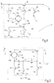
- In order to assist understanding of the present invention, a preferred embodiment is now described, purely by way of non-limiting example, with reference to the attached drawings, in which:
- figure 1 shows a general circuit diagram of a sampler according to the known art;
- figure 2 shows temporal developments of control signals supplied to the sampler in figure 1;
- figure 3 shows the circuit diagram of a first switch device according to the known art, used in the sampler in figure 1;
- figure 4 shows the circuit diagram of a second switch device according to the known art, used in the sampler in figure 1; and
- figure 5 shows the circuit diagram of a boosted switch device according to the present invention, used in the sampler in figure 1.
- In figure 5, 12" indicates as a whole a switch device according to the present invention.
- The
switch device 12" comprises asupply line 60 set to a supply potential VCC, typically approximately 3 V; aground line 62 set to a ground potential VGND, typically 0 V; anNMOS transistor 64 having a drain terminal connected to theinput terminal 2 of thesampler 1, a source terminal connected to thenode 8 of thesampler 1, and a gate terminal connected to afirst node 66; abootstrap capacitor 68 connected between a second and athird node 70, 72; aPMOS transistor 74 having a drain terminal connected to thefirst node 66, source and bulk terminals connected to the second node 70, and a gate terminal receiving the first negated control signal
NMOS transistor 76 having a drain terminal connected to thefirst node 66, a source terminal connected to theground line 62, and a gate terminal receiving the second control signal F2D; anNMOS transistor 78 having a drain terminal connected to thesupply line 60, a source terminal connected to the second node 70, and a gate terminal receiving the second control signal F2D; anNMOS transistor 80 having a drain terminal connected to thethird node 72, a source terminal connected to theground line 62, and a gate terminal receiving the second control signal F2D; and aCMOS transfer-gate switch 82 connected between theinput terminal 2 and thethird node 72, and formed by anNMOS transistor 84 and aPMOS transistor 86, having drain terminals connected to one another and to theinput terminal 2, source terminals connected to one another and to thethird node 72, and gate terminals receiving respectively the first control signal F1D and the first negated control signal
- The
switch device 12" operates as follows. - The
NMOS transistor 64 acts as a switch, and is on when the first control signal F1D is in the high logic state, and is off when the first control signal F1D is in the low logic state, whereas thebootstrap capacitor 68 acts as a floating battery. - When the control signal F2D is in the high logic state, and therefore, owing to the non-overlapping condition, the first control signal F1D is in the low logic state, the
NMOS transistors CMOS switch 82 is open, and thePMOS transistor 74 is off. Thus, thefirst node 66 is connected to theground line 62, and therefore keeps theNMOS transistor 64 off, whereas thebootstrap capacitor 68 is connected between thesupply line 60 and theground line 62, and therefore the supply voltage VCC is applied to the terminals of the bootstrap capacitor. In addition, since thebootstrap capacitor 68 is charged by means of theNMOS transistor 78 having its drain terminal biased to the supply voltage VCC, the source terminal of theNMOS transistor 78 can be taken to a voltage which is equivalent at the most to VCC-VTH, such that thebootstrap capacitor 68 is charged to a voltage equivalent to VCC-VTH. - On the other hand, when the first control signal F1D is in the high logic state, and the second control signal F2D is in the low logic state, the
NMOS transistors CMOS switch 82 is closed, and thePMOS transistor 74 is on, such that thebootstrap capacitor 68 is connected between theinput terminal 2 and the gate terminal of theNMOS transistor 64. - In particular, the
third node 72 is connected to theinput terminal 2, at which the input voltage VA is present, whereas at the second node 70, and therefore at the gate terminal of theNMOS transistor 64, a voltage equivalent to approximately VCC-VTH+VA is present. Thus, by this means, the gate-source voltage VGS and the gate-drain voltage VGD of theNMOS transistor 64 during conduction, are approximately constant, and equivalent to VCC-VTH, independently of the input voltage VA (bootstrapping effect of the gate-source voltage) and the potential of the gate terminal of theNMOS transistor 64 exceeds the supply voltage VCC supplied to theswitch device 12" (boosting effect of the gate terminal), with the advantages concerning linearisation of the series resistance RON of theNMS transistor 64 during conduction, previously described for the switch device 12'. - Thus, unlike the prior art switch device 12', in which the
bootstrap capacitor 48 is connected cyclically and in an alternating manner between theinput terminal 2 and theground line 16, and between thesupply line 54 and the gate terminal of theNMOS transistor 30, in theswitch device 12", thebootstrap capacitor 68 is connected cyclically and in an alternating manner between thesupply line 60 and theground line 62, and between theinput terminal 2 and the gate terminal of theNMOS transistor 64. - By this means, therefore, the
switch device 12" according to the present invention maintains the advantages of the switch device 12', but does not have the disadvantages of the latter. In fact, the variations in the input voltage VA are "seen" instantly on the gate terminal of theNMOS transistor 64, such that the gate-source voltage VGS of theNMOS transistor 64 always remains constant, irrespective of the maximum frequency of the input voltage VA, and therefore it is not necessary to limit the bandwidth thereof, such that it is possible to use the Nyquist sampling frequency, with the resulting benefits from the point of view of waste of power and area on the silicon. - In addition, in the
switch device 12" according to the invention, when the first control signal F1D is in the high logic state, the first and thesecond nodes 66 and 70 go to a voltage equivalent to VCC-VTH+VA, such that the problems of reliability, which arise only if VCC-VTH+VA is greater than the maximum operating voltage which can be withstood by integrated devices, are greatly reduced. In fact, considering again the example previously given, involving a technological process at 0.5 µm, in which the maximum operating voltage which can be withstood by integrated devices is equivalent to 4.6 V, with a supply voltage VCC equivalent to 3.3 V, in order for VCC-VTH+VA not to exceed the maximum operating voltage, it is necessary to limit the maximum input voltage VA to 2.3 V (on the assumption that VTH = 1 V), with a consequent gain in the signal/noise ratio of the A/D converter, in which theswitch device 12" is used, of 77%, compared with that which can be obtained using the prior art switch device 12'. - Finally, it is apparent that modifications and variants can be made to the
switch device 12" described, without departing from the protective context of the present invention, as defined in the attached claims.
Claims (13)
- Boosted switch device (12") comprising an input terminal (2) and an output terminal (8), first switch means (64) arranged between said input and output terminals (2, 8), and having a control terminal (66); a first line (62) set to a first potential (VGND); a second line (60) set to a second potential (VCC); and charge storage means (68); characterised in that it further comprises controlled connection means (74, 76, 78, 80, 82) connecting said charge storage means (68) in an alternating manner between said first and second lines (62, 60) and between said input terminal (2) and said control terminal (66).
- Boosted switch device according to claim 1, characterised in that said controlled connection means (74, 76, 78, 80, 82) connect said charge storage means (68) between said first and second lines (62, 60), when said first switch means (64) assume a first operating condition, and between said input terminal (2) and said control terminal (66), when said first switch means (64) assume a second operating condition.
- Boosted switch device according to claim 2, characterised in that said first operating condition is an opening condition of said first switch means (64), and said second operating condition is a closure condition of said first switch means (64).
- Boosted switch device according to any one of the preceding claims, characterised in that said controlled connection means (74, 76, 78, 80, 82) comprise second switch means (74) having a first terminal connected to said control terminal (66) of said first switch means (64), a second terminal connected to a first terminal (70) of said charge storage means (68), and a control terminal receiving a first control signal (

- Boosted switch device according to claim 4, characterised in that said first, second, third, fourth and fifth switch means (64, 74, 76, 78, 80) comprise respective MOS transistors, and said sixth switch means (82) comprise a CMOS switch receiving said first control signal (


- Boosted switch device according to claim 4 or claim 5, characterised in that said second and third control signals (F2D, F1D) do not overlap one another temporally.
- Boosted switch device according to any one of the preceding claims, characterised in that said charge storage means comprise a capacitor (68).
- Boosted switch device according to any one of the preceding claims, characterised in that said first line is a ground line (62) set to a ground potential (VGND), and said second line is a supply line (60) set to a supply potential (VCC).
- Sampler (1), characterised in that it comprises a boosted switch device (12") according to any one of the preceding claims.
- Sampler according to claim 9, characterised in that it further comprises an input terminal (2) connected to said input terminal (2) of said boosted switch device (12"), and further charge storage means (6) connected to said input terminal (2) of said sampler (2) via said boosted switch device (12").
- Operating method of a boosted switch device (12") comprising an input terminal (2) and an output terminal (8), first switch means (64) arranged between said input and output terminals (2, 8), and having a control terminal (66); a first line (62) set to a first potential (VGND); a second line (60) set to a second potential (VCC); and charge storage means (66); said method being characterised in that it comprises the step of:- connecting said charge storage means (68) in an alternating manner between said first and second lines (62, 60), and between said input terminal (2) and said control terminal (66).
- Method according to claim 11, characterised in that said connecting step comprises the steps of:- connecting said charge storage means (68) between said first and second lines (62, 60), when said first switch means (64) assume a first operating condition; and- connecting said charge storage means (68) between said input terminal (2) and said control terminal (66), when said first switch means (64) assume a second operating condition.
- Method according to claim 12, characterised in that said first operating condition is a opening condition of said first switch means (64), and said second operating condition is a closure condition of said first switch means (64).
Priority Applications (2)
| Application Number | Priority Date | Filing Date | Title |
|---|---|---|---|
| EP00830430A EP1168619A1 (en) | 2000-06-19 | 2000-06-19 | Boosted switch device for a sampler of an analogue/digital converter, and operating method thereof |
| US09/884,872 US6518901B2 (en) | 2000-06-19 | 2001-06-18 | Boosted switch device for a sampler of an analog/digital converter, and operating method thereof |
Applications Claiming Priority (1)
| Application Number | Priority Date | Filing Date | Title |
|---|---|---|---|
| EP00830430A EP1168619A1 (en) | 2000-06-19 | 2000-06-19 | Boosted switch device for a sampler of an analogue/digital converter, and operating method thereof |
Publications (1)
| Publication Number | Publication Date |
|---|---|
| EP1168619A1 true EP1168619A1 (en) | 2002-01-02 |
Family
ID=8175372
Family Applications (1)
| Application Number | Title | Priority Date | Filing Date |
|---|---|---|---|
| EP00830430A Withdrawn EP1168619A1 (en) | 2000-06-19 | 2000-06-19 | Boosted switch device for a sampler of an analogue/digital converter, and operating method thereof |
Country Status (2)
| Country | Link |
|---|---|
| US (1) | US6518901B2 (en) |
| EP (1) | EP1168619A1 (en) |
Cited By (3)
| Publication number | Priority date | Publication date | Assignee | Title |
|---|---|---|---|---|
| EP1494357A1 (en) * | 2003-07-03 | 2005-01-05 | STMicroelectronics S.r.l. | Boosted sampling circuit and relative method of driving |
| WO2005117260A1 (en) * | 2004-05-28 | 2005-12-08 | Koninklijke Philips Electronics N.V. | High voltage switch using low voltage cmos transistors |
| FR2871630A1 (en) * | 2004-06-11 | 2005-12-16 | Commissariat Energie Atomique | METHOD FOR CONTROLLING AN ANALOG SWITCH |
Families Citing this family (13)
| Publication number | Priority date | Publication date | Assignee | Title |
|---|---|---|---|---|
| ITMI20030154A1 (en) * | 2003-01-30 | 2004-07-31 | St Microelectronics Srl | COMMANDED SWITCH OF THE TYPE WITH SWITCHED CAPACITY. |
| US7015742B2 (en) * | 2003-06-20 | 2006-03-21 | Media Tek Inc. | Switched capacitor circuit capable of eliminating clock feedthrough by complementary control signals for digital tuning VCO |
| US7034736B1 (en) | 2004-11-02 | 2006-04-25 | Analog Devices, Inc. | Processing systems and methods that reduce even-order harmonic energy |
| CN101001085B (en) * | 2006-12-30 | 2010-05-12 | 深圳市芯海科技有限公司 | Signal sampling hold circuit |
| US7894151B2 (en) * | 2008-02-15 | 2011-02-22 | Broadcom Corporation | “Flat analog” AFE coupled with an all digital architecture compensation read channel |
| US8502594B2 (en) * | 2008-12-31 | 2013-08-06 | Linear Technology Corporation | Bootstrap transistor circuit |
| US7940091B1 (en) * | 2009-03-02 | 2011-05-10 | Linear Technology Corporation | Bootstrapped switch for sampling voltages beyond the supply voltage |
| CN102098034B (en) * | 2009-12-15 | 2014-07-30 | 北京中星微电子有限公司 | Bootstrap sampling circuit |
| US8674863B2 (en) * | 2011-06-07 | 2014-03-18 | Microchip Technology Incorporated | Distributed bootstrap switch |
| US8593181B2 (en) * | 2011-08-04 | 2013-11-26 | Analog Devices, Inc. | Input switches in sampling circuits |
| US9218513B2 (en) * | 2012-12-21 | 2015-12-22 | Sequans Communications | Circuit and method with improved mixer linearity |
| US10601435B2 (en) * | 2018-05-23 | 2020-03-24 | Mediatek Inc. | Initial booting bootstrap circuit and associated analog-to-digital converter |
| JP7742547B2 (en) * | 2021-02-22 | 2025-09-22 | パナソニックIpマネジメント株式会社 | Gate drive circuit, gate drive device, high frequency power supply device and system |
Citations (1)
| Publication number | Priority date | Publication date | Assignee | Title |
|---|---|---|---|---|
| US6072355A (en) * | 1998-01-22 | 2000-06-06 | Burr-Brown Corporation | Bootstrapped CMOS sample and hold circuitry and method |
Family Cites Families (4)
| Publication number | Priority date | Publication date | Assignee | Title |
|---|---|---|---|---|
| US5500612A (en) * | 1994-05-20 | 1996-03-19 | David Sarnoff Research Center, Inc. | Constant impedance sampling switch for an analog to digital converter |
| US5945872A (en) * | 1997-11-06 | 1999-08-31 | Analog Devices, Inc. | Two-phase boosted CMOS switch drive technique and circuit |
| US6310565B1 (en) * | 2000-02-03 | 2001-10-30 | Lucent Technologies Inc. | Sampling switch having an independent “on” impedance |
| US6323697B1 (en) * | 2000-06-06 | 2001-11-27 | Texas Instruments Incorporated | Low distortion sample and hold circuit |
-
2000
- 2000-06-19 EP EP00830430A patent/EP1168619A1/en not_active Withdrawn
-
2001
- 2001-06-18 US US09/884,872 patent/US6518901B2/en not_active Expired - Lifetime
Patent Citations (1)
| Publication number | Priority date | Publication date | Assignee | Title |
|---|---|---|---|---|
| US6072355A (en) * | 1998-01-22 | 2000-06-06 | Burr-Brown Corporation | Bootstrapped CMOS sample and hold circuitry and method |
Cited By (6)
| Publication number | Priority date | Publication date | Assignee | Title |
|---|---|---|---|---|
| EP1494357A1 (en) * | 2003-07-03 | 2005-01-05 | STMicroelectronics S.r.l. | Boosted sampling circuit and relative method of driving |
| US6977544B2 (en) | 2003-07-03 | 2005-12-20 | Stmicroelectronics S.R.L. | Boosted sampling circuit and relative method of driving |
| WO2005117260A1 (en) * | 2004-05-28 | 2005-12-08 | Koninklijke Philips Electronics N.V. | High voltage switch using low voltage cmos transistors |
| FR2871630A1 (en) * | 2004-06-11 | 2005-12-16 | Commissariat Energie Atomique | METHOD FOR CONTROLLING AN ANALOG SWITCH |
| EP1608069A3 (en) * | 2004-06-11 | 2006-04-26 | Commissariat A L'energie Atomique | Method for controling an analog switch |
| US7274222B2 (en) | 2004-06-11 | 2007-09-25 | Commissariat A L'energie Atomique | Control method for an analogue switch |
Also Published As
| Publication number | Publication date |
|---|---|
| US20020021162A1 (en) | 2002-02-21 |
| US6518901B2 (en) | 2003-02-11 |
Similar Documents
| Publication | Publication Date | Title |
|---|---|---|
| US6518901B2 (en) | Boosted switch device for a sampler of an analog/digital converter, and operating method thereof | |
| US6060937A (en) | Two-phase bootstrapped CMOS switch drive technique and circuit | |
| US6323697B1 (en) | Low distortion sample and hold circuit | |
| EP0875904B1 (en) | A sample-and-hold circuit | |
| EP0060026B1 (en) | Gain stage with operational amplifier and switched capacitor resistor equivalent circuit | |
| US5945872A (en) | Two-phase boosted CMOS switch drive technique and circuit | |
| US6897701B2 (en) | Method and structure for improving the linearity of MOS switches | |
| EP0308007B1 (en) | A circuit arrangement for storing sampled analogue electrical currents | |
| US6977544B2 (en) | Boosted sampling circuit and relative method of driving | |
| US4931668A (en) | MIS transistor driven inverter circuit capable of individually controlling rising portion and falling portion of output waveform | |
| US7049877B2 (en) | Switched level-shift circuit | |
| Ong et al. | A method for reducing the variation in" on" resistance of a MOS sampling switch | |
| EP0308008A2 (en) | A method of and a circuit arrangement for processing sampled analogue electrical signals | |
| US6781434B2 (en) | Low charge-dump transistor switch | |
| US6429692B1 (en) | High speed data sampling with reduced metastability | |
| Munoz et al. | Analogue switch for very low-voltage applications | |
| WO2009153921A1 (en) | Analog switch | |
| US5767708A (en) | Current integrator circuit with conversion of an input current into a capacitive charging current | |
| US7372319B1 (en) | Constant boosted voltage generator circuit for feedback switches in a switched capacitor circuit | |
| JPH09284096A (en) | Switched capacitor circuit | |
| US6833753B2 (en) | Method and system for signal dependent boosting in sampling circuits | |
| US6404262B1 (en) | Switched capacitor integrator using unity gain buffers | |
| EP0101947B1 (en) | Driving circuit | |
| KR900002804B1 (en) | Conservation circuit for high potential | |
| CN116346111A (en) | A Gate Voltage Bootstrap Switching Circuit Based on PMOS Transistor |
Legal Events
| Date | Code | Title | Description |
|---|---|---|---|
| PUAI | Public reference made under article 153(3) epc to a published international application that has entered the european phase |
Free format text: ORIGINAL CODE: 0009012 |
|
| AK | Designated contracting states |
Kind code of ref document: A1 Designated state(s): AT BE CH CY DE DK ES FI FR GB GR IE IT LI LU MC NL PT SE Kind code of ref document: A1 Designated state(s): DE FR GB IT |
|
| AX | Request for extension of the european patent |
Free format text: AL;LT;LV;MK;RO;SI |
|
| 17P | Request for examination filed |
Effective date: 20020610 |
|
| AKX | Designation fees paid |
Free format text: DE FR GB IT |
|
| 17Q | First examination report despatched |
Effective date: 20060718 |
|
| GRAP | Despatch of communication of intention to grant a patent |
Free format text: ORIGINAL CODE: EPIDOSNIGR1 |
|
| STAA | Information on the status of an ep patent application or granted ep patent |
Free format text: STATUS: THE APPLICATION IS DEEMED TO BE WITHDRAWN |
|
| 18D | Application deemed to be withdrawn |
Effective date: 20080327 |