EP0308007B1 - A circuit arrangement for storing sampled analogue electrical currents - Google Patents
A circuit arrangement for storing sampled analogue electrical currents Download PDFInfo
- Publication number
- EP0308007B1 EP0308007B1 EP88201933A EP88201933A EP0308007B1 EP 0308007 B1 EP0308007 B1 EP 0308007B1 EP 88201933 A EP88201933 A EP 88201933A EP 88201933 A EP88201933 A EP 88201933A EP 0308007 B1 EP0308007 B1 EP 0308007B1
- Authority
- EP
- European Patent Office
- Prior art keywords
- current
- output
- input
- circuit arrangement
- transistor
- Prior art date
- Legal status (The legal status is an assumption and is not a legal conclusion. Google has not performed a legal analysis and makes no representation as to the accuracy of the status listed.)
- Expired - Lifetime
Links
Images


Classifications
-
- G—PHYSICS
- G11—INFORMATION STORAGE
- G11C—STATIC STORES
- G11C27/00—Electric analogue stores, e.g. for storing instantaneous values
-
- G—PHYSICS
- G11—INFORMATION STORAGE
- G11C—STATIC STORES
- G11C27/00—Electric analogue stores, e.g. for storing instantaneous values
- G11C27/02—Sample-and-hold arrangements
- G11C27/024—Sample-and-hold arrangements using a capacitive memory element
- G11C27/028—Current mode circuits, e.g. switched current memories
-
- H—ELECTRICITY
- H03—ELECTRONIC CIRCUITRY
- H03F—AMPLIFIERS
- H03F3/00—Amplifiers with only discharge tubes or only semiconductor devices as amplifying elements
- H03F3/45—Differential amplifiers
- H03F3/45071—Differential amplifiers with semiconductor devices only
- H03F3/45076—Differential amplifiers with semiconductor devices only characterised by the way of implementation of the active amplifying circuit in the differential amplifier
Landscapes
- Engineering & Computer Science (AREA)
- Power Engineering (AREA)
- Analogue/Digital Conversion (AREA)
- Amplifiers (AREA)
- Filters That Use Time-Delay Elements (AREA)
- Charge And Discharge Circuits For Batteries Or The Like (AREA)
Description
- The invention relates to a circuit arrangement for storing sampled analogue electrical currents.
- For processing analogue signals using circuitry which can be easily integrated the switched capacitor technique has been used. Since it is difficult to integrate large valued resistors because of the area occupied and further the correlation between resistor and capacitor values produced by integration is not good causing the resultant time constants to be poorly defined, the technique of using the equivalent resistance of a capacitor which is switched into and out of circuit to cause processing to take place by means of manipulation of charge packets has been used for analogue signal processing where integration has been required.
- Although they are widely used, switched capacitor circuits have certain disadvantages. It is necessary to produce capacitors which are linear, that is their capacitance should not change significantly with the signal level. This has been achieved in CMOS integrated circuits by providing two polysilicon layers for the plates of the capacitors. However standard CMOS processes used for the integration of digital circuits do not employ a double polysilicon layer. Consequently switched capacitor circuits which are formed on the same chip as digital circuits require additional processing steps. In switched capacitor circuits the double polysilicon layer switched capacitors together with the required compensation capacitors for the operational amplifiers can account for a significant proportion of the total silicon area. This tends to produce relatively large chips. Further in most switched capacitor systems, each amplifier and switch must be individually designed and optimised for its particular environment in order for the circuit to perform adequately.
- Our co-pending Application GB-A-2213011 (PHB33385) discloses a method of processing sampled analogue electrical signals comprising the steps of
- a) converting each sample into a current, if it is not already in that form;
- b) combining, in predetermined proportions, the input sample current in the present sample period with current(s) derived from input sample current(s) in one or more preceding sample periods, and
- c) deriving the processed output signal from the combined current produced by step b) in successive sample periods.
- This method is based on the realisation that the quantity manipulated can be current rather than, as is the case with switched capacitor circuits, charge. The choice of manipulated quantity variable to be current rather than charge characterises the method. Thus in a switched capacitor circuit the signal processing is achieved by adding, subtracting or storing electrical charges whereas in the method set out hereinbefore, referred to hereinafter as switched current signal processing, the signal processing is achieved by scaling, adding, subtracting or storing electrical current samples. Considerable similarities exist in the processing of the electrical quantities although the actual electrical quantity manipulated is different. In particular all the mathematics concerned with the application of Z-transforms to switched capacitor circuits is equally valid for those employing current as the manipulated quantity.
- The choice of current as the manipulated quantity enables a number of advantages to be obtained. The technique does not require high quality linear capacitors. As a direct consequence, it may be possible to dispense with the second polysilicon layer used in switched capacitor circuits to fabricate linear capacitors. In that case standard CMOS processes used for the integration of digital circuits may be used for the implementation of circuits employing the method. This gives true VLSI compatability. Since the large area double polysilicon layer switched capacitors are not required and the only requirement for capacitors for the new method is for capacitors which have a small value and have a monotomic charge/voltage relationship which need not be linear and which may be realised as gate oxide or diffusion capacitors. Thus, for a given function the implementation will be smaller than its switched capacitor counterpart. Further reduction in the chip area may also result from the use of smaller geometry MOS processes. Circuits designed in older, coarser, processes may be able to take advantage of developments in mask making and etching technologies by geometric shrinkage of the layout. Geometric shrinkage is not generally feasible in switched capacitor circuits since circuit parameters such as amplifier settling time and switch resistance can change detrimentally even though the channel width/length ratio of the MOS devices is held constant.
- In a switched capacitor system, each amplifier and switch must be individually designed and optimised for its particular environment in order for the circuit to perform adequately. In contrast with the switched current signal processing method, the nature of operation allows the two basic circuit elements required, that is a family of low input impedance high output impedance current mirrors and analogue current memory, to be designed once only for each IC process. It will, of course, be necessary to design a separate current mirror for each scaling factor. Thus once a particular system configuration has been converged upon, the time spent on circuit design for implementation in the new technique may be significantly reduced compared with that required for a switched capacitor approach. The independent cellular nature of the circuitry enabled by the switched current signal processing method opens the way for semi-custom design procedures to be applied.
- The principal disadvantage of this method is a consequence of its discrete time operation. As in a switched capacitor signal processing system or any system in which signal sampling is performed, some form of anti-aliasing filtering is required before the first sample and hold operation. Apart from representing an increase in complexity of total circuit function, the VLSI compatability of the technique is threatened if the anti-alias filter requires a second polysilicon layer or other process modification for its monolithic implementation.
- In order to implement the method disclosed in our co-pending Application G-A-2213011 (PHB33385) a circuit arrangement for storing a sampled analogue current is required and consequently it is an object of the invention to enable the provision of such a circuit arrangement.
- The invention provides a circuit arrangement for storing sampled analogue electrical currents comprising a current input, a current output, first and second switches controlled by first and second non-overlapping clock signals, and first and second current storage cells, wherein the current input is coupled to the first storage cell by means of the first switch and the first storage cells is coupled to the second storage cell by means of the second switch, the output of the second storage cell being coupled to the current output.
- The output of the arrangement can be considered valid whenever the second switch is open. Clearly the output current may have a changing value when the second switch is closed as it will take a finite time for the current in the second storage cell to settle where there is a difference in currents in successive sampling periods.
- Each storage cell may comprise a field effect transistor having a capacitor connected between its gate and source electrodes. Thus provided that the sampling frequency is sufficiently high the gate-source voltage of the transistors will be held constant by the charge on the capacitor and so maintain the output current constant.
- In each storage cell the field effect transistor may form an output branch of a current mirror circuit. The first and second switches may be arranged to isolate the input and output branches of the current mirrors, the output branch of the first current mirror being connected to the input branch of the second current mirror.
- The provision of the switches between the current branches of the current mirrors enables the isolation of the two branches whilst providing a current path for the output of the first storage cell when the second switch is open.
- At least one of the current mirror circuits may have a non-unity current ratio between its input and output branches. The second current mirror may have a plurality of output branches.
- This enables the arrangement to have a current gain which differs from unity and to have a fan-out capability to enable various circuit functions to be implemented.
- An embodiment of the invention will now be described, by way of example, with reference to the accompanying drawings, in which:-
- Figure 1 is a circuit diagram of an embodiment of a circuit arrangement according to the invention for storing sampled analogue signals,
- Figure 2 shows clock signals for controlling the switches in the embodiment of Figure 1,
- Figure 3 shows in block schematic form an integrator in which a circuit arrangement according to the invention is incorporated,
- Figure 4 is a first transistor level embodiment of the integrator shown in Figure 3,
- Figure 5 is a second transistor level embodiment of the integrator shown in Figure 3 having provision for signals of both positive and negative polarity,
- Figure 6 shows curves illustrating the response of the integrator shown in Figure 5, and,
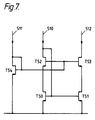
- Figure 7 shows an embodiment of a current mirror suitable for use in the integrator shown in Figure 3, 4 or 5.
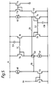
- The circuit arrangement shown in Figure 1 has a
current input 1 which is connected to the input branch of a first current mirror circuit formed by two p-channel field effect transistors (FETs) T4 and T8. The gate electrodes of FETs T4 and T8 are coupled by a switch S1 controlled by a clock signal ØA which is shown in Figure 2. A capacitor CA is connected between the gate and source electrodes of FET T8 and is isolated from the gate of FET T4 by the switch S1. The drain of FET T8 which forms the output branch of the first current mirror circuit is connected to the drain electrode of an n-channel FET T9 which forms the input branch of a second current mirror circuit whose output branch is formed by an n-channel FET T12 whose drain electrode is connected to thecurrent output 6. The gate electrodes of FETs T9 and T12 are coupled by a switch S2 controlled by a clock signal ØB which is shown in Figure 2. A capacitor CB is connected between the gate and source electrodes of FET T12 and is isolated from the gate of FET T9 by the switch S2. - In operation an input current sample is fed to input 1 during sample period Pn and during clock ØA switch S1 is closed and hence the input current applied to the drain of FET T4 is mirrored at the drain of FET T8. At the same time the capacitor CA becomes charged to the gate/source voltage of FET T8. At the end of the period ØA in the sample period Pn the switch S1 opens but the current through FET T8 is maintained due to the charge on capacitor CA. When the non-overlapping clock signal ØB occurs during sample period Pn the switch S2 is closed and the drain current of FET T12 mirrors that of the FET T9. At the same time the capacitor CB is charged to the gate/source potential of FET T12. At the end of the period ØB in the sample period Pn the switch S2 opens but the current through FET T12 is maintained due to the charge on capacitor CB. Thus from the end of the clock period ØB in sample period Pn until the beginning of the clock period ØB in sample period Pn+1 the output current provided by the circuit arrangement is equal to the input current during the clock period ØA in sample period Pn.
- Thus if we define the true state of the current to be that during each ØA clock in each sample period then the relationship between the input Ii and output Io currents can be written

- Clearly an input current could be stored for more than one sample period by cascading the circuit arrangement shown in Figure 1. Alternatively if a new input sample is not to be applied in every sample period then appropriate choice of clock signal waveforms ØA and ØB could provide a greater than one sample period storage. Further by selective feedback of the output current to the input greater than one sample period storage could be achieved. That is a recirculating memory may be formed by connecting the
output 6 to theinput 1. - The circuit arrangement shown in Figure 1 can be used to provide a one sample period delay of the input current or to provide a multiple sample period delay by cascading a plurality of such arrangements. A less than one sample period delay could be achieved by providing a second output branch on the current mirror formed by FETs T4 and T8 and appropriately clocking the second output branch, for example using clock ØB.
- If it is desired to make the input and output current equal then both current mirrors can have a unity current ratio or they could have non-unity but complementary current ratios. If the desired output current is to be a multiple or submultiple of the input current then this can be achieved by appropriate choice of the current ratios of the current mirrors.
- The choice of current ratios can be achieved in conventional fashion by choice of dimensions of the FETs or choice of source degeneration resistor values.
- Figure 3 shows an integrator comprising a circuit arrangement as shown in Figure 1 which in the subsequent description with reference to Figures 3 to 5 will be referred to as a
current memory 54, a firstcurrent mirror circuit 52, a secondcurrent mirror circuit 55 and a summingnode 53. The integrator has aninput 51 for receiving an input signal in the form of a sampled current and anoutput 56 at which the integrated input becomes available. - In operation, current samples are fed to the
input 51 and the input current sample is reproduced at the output of thecurrent mirror 52. Assuming that the integrator is reset to zero, when the first current pulse occurs it is stored in thecurrent memory 54. The input current sample applied to theinput 51 in the next sample period will then be summed with the current at the output of thecurrent mirror 55. The current at the output of thecurrent mirror 55 will be that stored in thecurrentmemory 54 during the previous sample period. The summed current at the summingnode 53 is then fed to the input ofcurrent memory 54. Thus during the first sample period the output of the integrator will be at zero. During the second sample period, the output of thecurrent memory 54 will be equal to the current applied during the first sample period and hence the output of the integrator will also be equal to the current applied during the first sample period. Also, during the second sample period the input of thecurrent memory 54 will receive the sum of the current during the second sampling period and the current during the first sampling period derived from the output of thecurrent memory 54 and hence during the third sampling period the output of the integrator, which is assumed equal to the output of thecurrent memory 54, will be equal to the current during the first sampling period plus the current during the second sampling period. Thus this arrangement will continuously add the sample currents in successive sample periods and produce at the output the sum of the currents in each of the sampling periods that have occurred since the integrator was reset. This assumes that the gains of bothcurrent mirrors current mirror 55 is set to be less than one. If it is assumed that the gain of thecurrent mirror 52 is equal to α and the gain of thecurrent mirror 55 is equal to β and that n sampling periods have elapsed since the integrator was set to zero, then the current output of the integrator during the nth period

- Figure 6 shows the response of the integrator shown in Figure 3 where α is set to 0.5 and in the first case β is set to 1 and in the second case β is set to 0.8. The first case illustrates an ideal integrator and the second a lossy integrator.
- Figure 4 is a transistor level circuit diagram of an integrator of the form shown in Figure 3. As shown in Figure 4 the
current mirror 52 is formed from two field effect transistors (FETs) T1 and T2. The output of thecurrent mirror 52, which is formed by the drain of transistor T2, is connected to the summingjunction 53. The source of transistor T4 is the input of thecurrent memory 54. The current memory comprises the transistors T4, T8, T6, and T9; the capacitors CA and CB; and two switches S1 and S2. The switches S1 and S2 are operated by pulses ØA and ØB from the clock generator 9. These pulses are non-overlapping and occur at the sampling rate, that is there is a ØA and a ØB pulse in each sample period. Assuming that the integrator is reset, the input signal current applied in one sampling period to theinput 51 is mirrored at the output of transistor T2 applied to the summingjunction 53 and hence to the input of thecurrent memory 54. During a first portion ØA of the sample period, the switch S1 is closed and hence the transistor T8 will mirror the current applied to the transistor T4. At the same time the capacitor CA will charge to the gate source potential of the transistor T8 and also of the transistor T4. When the switch S1 is opened at the end of the first portion ØA the charge on the capacitor CA maintains the gate source potential of transistor T8 and hence the current flowing through it. During a second non-overlapping portion ØB of the sample periodd the switch S2 is closed and the transistors T9 and T6 then form a current mirror, transistor T9 being the input branch and transistor T6 the output branch. During the period ØB when the switch S2 is closed, the output current produced by transistor T6 mirrors the input current applied to transistor T9 and at the same time the capacitor CB is charged to the gate-source potential of the transistor T6. Consequently, when the switch S2 opens, the current through transistor T6 is maintained by the voltage stored on the capacitor CB. Thus the output for period (n-1) is held on transistor T6 until the period ØB in the sampling period n. The gate-source potential of transistor T12 is also determined by the charge on capacitor CB and the output current of the integrator is derived from the current through transistor T12. This will be proportional to the current through transistor T6, The constant of proportionality depending on the dimensions of transistors T6 and T12. - In the embodiment shown in Figure 4, the
current mirror 52 is formed by transistors T1 and T2; thecurrent memory 54 is formed by transistors T4, T8, T6, T9, capacitors CA and CB, and switches S1 and S2; and thecurrent mirror 55 is formed by the capacitor CB and transistors T6 and T12. During the period ØB the transistor T9 also forms a part of thecurrent mirror 55. - The circuit shown in Figure 4 is suitable only for currents which are uni-directional. In order to cater for signals which have positive and negative values with respect to a reference and thus give rise to bi-directional input currents, the input current is added to a bias current Ibias which allows the input current to have a peak to peak range of ±Ibias, assuming that the circuits are designed to handle a peak current of 2Ibias, while presenting a unidirectional current to the
input 51. The arrangement shown in Figure 5 is similar to that shown in Figure 4 but is provided with additional sources of bias current to enable a bi-directional input current superimposed on a bias current to be processed and an output to be produced having a similar form i.e. a bi-directional signal current superimposed on the bias current Ibias. In Figure 5, those components having the same function as components in Figure 4 have been given the same reference signs. - The circuit shown in Figure 5 has a
current source 60 connected between the drain of transistor T2 and the positive supply rail. Thecurrent source 60 provides a current α Ibias, where α is the gain of the current mirror comprising transistors T1 and T2. Consequently if an input current Ibias + i is applied to input 51 a current

junction 53 overline 70. A further current source 61 is connected between the negative supply rail and the summingjunction 53. Since the current α i is bi-directional it is necessary to superimpose it on a bias current to prevent the diode connected transistor T4 at the input of the current memory from being reverse biassed. The current source 61 is arranged to produce a current Ibias which is added to the current α i on theline 70. Thecurrent memory 54 comprises first and second switched current mirrors formed by transistors T4 and T8 and T9 and T6, respectively. The second current mirror formed by transistors T9 and T6 also form thecurrent mirror 55 and is arranged so that trasistor T6 produces the current β Imem and that transistor T12 produces the current Imem. The current Imem is equal to io + Ibias where io is the integrated input current. - Since the current Imem includes the bias current and hence the current β Imem includes β Ibias it is necessary to subtract the current β Ibias from the current produced by transistor T6 and fed back over
line 72 to the summingjunction 53 to prevent the bias current from being integrated as well as the signal current. Consequently acurrent source 62 is connected between the positive supply rail and the drain of transistor T6, thecurrent source 62 being arranged to produce the current β Ibias which is subtracted from the current produced by transistor T6. - It should be noted that the current ratio between transistors T9 and T12 is 1:1 and hence the current produced by transistor T12 is equal to Imem and consequently is io + Ibias. The current mirror formed by transistors T13 and T14 is arranged to have a 1:1 current ratio and is provided merely to invert the direction of the output current to match that of the input current. Its presence is optional depending on the function required and consequently the output current may be taken from the drain of transistor T12 if inversion of the output current with respect to the input is required.
- For best performance, the
current mirrors - The current mirror circuit shown in Figure 7 has an input on
line 510. The current mirror is formed by two cascoded transistors T50 and T52 in the input branch and two further cascoded transistors T51 and T53 in the output branch, the output being derived fromline 512. A further branch comprising a transistor T54 and having an input online 511 is provided to produce a bias current for the transistors T52 and T53. The transistor T54 has a gate width to length ratio of a quarter of that of the transistors T52 and T53. It is possible to extend the cascoding of the transistors in the branches of the current mirror. A third cascoded transistor may be connected, in which case a further bias branch is required to bias the third transistors in the input and output branches. The transistor in the further bias branch having a gate width to length ratio of 1/9th of that of the third transistors. These biassing arrangement give a maximum dynamic range for the input signals to the current mirror. If a maximum dynamic range is not required the cascoded transistors may be fed from a fixed biassed potential. A further modification which may be made to the current mirrors to improve their performance is dynamic element matching by means of which the input and output branches are continuously interchanged at a given clocking rate and an average output current derived. This technique may be used to compensate for mismatching in the transistors between the two branches of the current mirror. Dynamic element matching has been described in an article entitled "Dynamic Element Matching puts Trimless Converters on Chip" by Rudy van de Plassche in "Electronics"dated 16th June 1983. - The invention has been described with application to both an ideal and a lossy integrator, however the field of application of the invention extends beyond this particular type of circuit. For example, any signal processing circuit which can be fabricated by means of switched capacitor techniques will have an equivalent arrangement using the technique according to the invention which is referred to herein as the switched current technique. Thus the manipulation of charges in a switched capacitor type circuit can be replaced by the manipulation of currents in a switched current type circuit. Just as charges can be added and subtracted on a sampled basis, so can currents be added and subtracted on a sampled basis.
- From reading the present disclosure, other modifications will be apparent to persons skilled in the art. Such modifications may involve other features which are already known in the design, manufacture and use of sampled analogue electrical signal processing systems and devices and component parts thereof and which may be used instead of or in addition to features already described herein. Although claims have been formulated in this application to particular combinations of features, it should be understood that the scope of the disclosure of the present application also includes any novel feature or any novel combination of features disclosed herein either explicitly or implicitly or any generalisation thereof, whether or not it relates to the same invention as presently claimed in any claim and whether or not it mitigates any or all of the same technical problems as does the present invention. The applicants hereby give notice that new claims may be formulated to such features and/or combinations of such features during the prosecution of the present application or of any further application derived therefrom.
Claims (6)
- A circuit arrangement for storing sampled analogue electrical currents comprising a current input, a current output, first and second switches controlled by first and second non-overlapping clock signals, and first and second current storage cells, wherein the current input is coupled to the first storage cell by means of the first switch and the first storage cell is coupled to the second storage cell by means of the second switch, the output of the second storage cell being coupled to the current output.
- A circuit arrangement as claimed in Claim 1, in which each storage cell comprises a field effect transistor having a capacitor connected between its gate and source electrodes.
- A circuit arrangement as claimed in Claim 2, in which in each storage cell the field effect transistor forms an output branch of a current mirror circuit.
- A circuit arrangement as claimed in Claim 3, in which the first and second switches are arranged to isolate the input and output branches of the current mirrors, the output branch of the first current mirror being connected to the input branch of the second current mirror.
- A circuit arrangement as claimed in Claim 3 or Claim 4, in which at least one of the current mirror circuits has a non-unity current ratio between its input and output branches.
- A circuit arrangement as claimed in any of Claims 3 to 5, in which the second current mirror has a plurality of output branches.
Applications Claiming Priority (2)
| Application Number | Priority Date | Filing Date | Title |
|---|---|---|---|
| GB8721759 | 1987-09-16 | ||
| GB8721759A GB2209895B (en) | 1987-09-16 | 1987-09-16 | A circuit arrangement for storing sampled analogue electrical currents |
Publications (3)
| Publication Number | Publication Date |
|---|---|
| EP0308007A2 EP0308007A2 (en) | 1989-03-22 |
| EP0308007A3 EP0308007A3 (en) | 1990-09-05 |
| EP0308007B1 true EP0308007B1 (en) | 1994-01-19 |
Family
ID=10623864
Family Applications (1)
| Application Number | Title | Priority Date | Filing Date |
|---|---|---|---|
| EP88201933A Expired - Lifetime EP0308007B1 (en) | 1987-09-16 | 1988-09-07 | A circuit arrangement for storing sampled analogue electrical currents |
Country Status (6)
| Country | Link |
|---|---|
| US (1) | US4866368A (en) |
| EP (1) | EP0308007B1 (en) |
| JP (1) | JP2835347B2 (en) |
| KR (1) | KR950014095B1 (en) |
| DE (1) | DE3887240T2 (en) |
| GB (1) | GB2209895B (en) |
Families Citing this family (24)
| Publication number | Priority date | Publication date | Assignee | Title |
|---|---|---|---|---|
| GB2225885A (en) * | 1988-12-08 | 1990-06-13 | Philips Electronic Associated | Integrator circuit |
| GB2225912B (en) * | 1988-12-08 | 1993-09-08 | Philips Electronic Associated | Current mirror circuit |
| GB2225910A (en) * | 1988-12-08 | 1990-06-13 | Philips Electronic Associated | Processing sampled analogue electrical signals |
| GB2228351A (en) * | 1989-02-17 | 1990-08-22 | Philips Electronic Associated | Circuit arrangement for processing sampled analogue electrical signals |
| GB2231423A (en) * | 1989-05-10 | 1990-11-14 | Philips Electronic Associated | Integrator circuit |
| GB2231424A (en) * | 1989-05-10 | 1990-11-14 | Philips Electronic Associated | Integrator circuit |
| GB2235799A (en) * | 1989-09-06 | 1991-03-13 | Philips Electronic Associated | Differentiator circuit |
| JP2768070B2 (en) * | 1991-08-02 | 1998-06-25 | 日本電気株式会社 | Phase comparator |
| US5205647A (en) * | 1991-10-09 | 1993-04-27 | Acrison, Inc. | Fluid mixing apparatus and method of mixing |
| GB9204763D0 (en) * | 1992-03-05 | 1992-04-15 | Philips Electronics Uk Ltd | Signal processing arrangements |
| DE4216712A1 (en) * | 1992-05-20 | 1993-11-25 | Siemens Ag | Switchable current source circuit and use of such in a phase detector arrangement |
| KR100299597B1 (en) * | 1993-02-12 | 2001-10-22 | 요트.게.아. 롤페즈 | Integrated circuit with cascode current mirror |
| GB9500648D0 (en) * | 1995-01-13 | 1995-03-08 | Philips Electronics Uk Ltd | Switched current differentiator |
| US5760616A (en) * | 1995-09-05 | 1998-06-02 | Lucent Technologies, Inc. | Current copiers with improved accuracy |
| DE19545556A1 (en) * | 1995-12-06 | 1997-06-12 | Siemens Ag | Field effect transistor |
| FR2774232B1 (en) * | 1998-01-26 | 2000-02-25 | Alsthom Cge Alcatel | DEVICE FOR GENERATING LOW NOISE CURRENT PULSES, PHASE COMPARATOR, SYNTHESIZER AND USE THEREOF |
| GB9812739D0 (en) * | 1998-06-12 | 1998-08-12 | Koninkl Philips Electronics Nv | Active matrix electroluminescent display devices |
| GB0421535D0 (en) * | 2004-09-28 | 2004-10-27 | Imp College Innovations Ltd | Sample and hold circuits |
| US7187215B2 (en) * | 2005-01-12 | 2007-03-06 | Agilent Technologies | High dynamic range current-mode track-and-hold circuit |
| KR100757431B1 (en) * | 2006-02-28 | 2007-09-11 | 엘지전자 주식회사 | Analog switch circuit and method for minimizing on-resistance of a sampling switch |
| DE102007036973A1 (en) * | 2007-02-24 | 2008-09-04 | Fraunhofer-Gesellschaft zur Förderung der angewandten Forschung e.V. | A pixel cell, a method of operating a pixel cell, a method of determining a position of a maximum of an envelope of an analog amplitude modulated signal, a device for determining a charge amount, apparatus and method for determining an amount of charge on a capacitive element, apparatus and method, and setting a circuit node a predetermined voltage, apparatus and method for charge-based analog / digital conversion and apparatus and method for charge-based signal processing |
| DE102010001154A1 (en) * | 2010-01-22 | 2011-07-28 | Robert Bosch GmbH, 70469 | Device and method for generating a current pulse |
| US20130154714A1 (en) * | 2011-12-20 | 2013-06-20 | Conexant Systems, Inc. | Current-mode sample and hold for dead time control of switched mode regulators |
| US10009971B2 (en) * | 2015-07-23 | 2018-06-26 | Cree, Inc. | Lighting apparatus using multiple LED strings with current mirror circuitry and methods of operating same |
Family Cites Families (9)
| Publication number | Priority date | Publication date | Assignee | Title |
|---|---|---|---|---|
| JPS55163694A (en) * | 1979-06-01 | 1980-12-19 | Fujitsu Ltd | Sample holding circuit |
| US4323796A (en) * | 1980-01-30 | 1982-04-06 | Motorola, Inc. | Low transient feedthru FET sample and hold gate |
| US4458200A (en) * | 1982-11-01 | 1984-07-03 | Gte Laboratories Incorporated | Reference voltage source |
| US4585951A (en) * | 1983-10-24 | 1986-04-29 | Motorola, Inc. | Precision triangle waveform generator |
| NL8401311A (en) * | 1984-04-24 | 1985-11-18 | Philips Nv | LOAD-COUPLED SEMICONDUCTOR WITH DYNAMIC CONTROL. |
| US4583037A (en) * | 1984-08-23 | 1986-04-15 | At&T Bell Laboratories | High swing CMOS cascode current mirror |
| DE3685501T2 (en) * | 1985-02-04 | 1993-01-28 | Sony Corp | SCAN AND STOP CIRCUIT. |
| US4604584A (en) * | 1985-06-10 | 1986-08-05 | Motorola, Inc. | Switched capacitor precision difference amplifier |
| IT1184820B (en) * | 1985-08-13 | 1987-10-28 | Sgs Microelettronica Spa | SINGLE POWER STABILIZED CURRENT GENERATOR, ESPECIALLY FOR MOS TYPE INTEGRATED CIRCUITS |
-
1987
- 1987-09-16 GB GB8721759A patent/GB2209895B/en not_active Expired - Lifetime
-
1988
- 1988-09-07 EP EP88201933A patent/EP0308007B1/en not_active Expired - Lifetime
- 1988-09-07 DE DE3887240T patent/DE3887240T2/en not_active Expired - Fee Related
- 1988-09-14 US US07/244,439 patent/US4866368A/en not_active Expired - Lifetime
- 1988-09-14 JP JP63228866A patent/JP2835347B2/en not_active Expired - Fee Related
- 1988-09-16 KR KR1019880011963A patent/KR950014095B1/en not_active IP Right Cessation
Also Published As
| Publication number | Publication date |
|---|---|
| DE3887240D1 (en) | 1994-03-03 |
| JP2835347B2 (en) | 1998-12-14 |
| EP0308007A3 (en) | 1990-09-05 |
| DE3887240T2 (en) | 1994-07-21 |
| JPH01102797A (en) | 1989-04-20 |
| GB2209895A (en) | 1989-05-24 |
| KR890005754A (en) | 1989-05-16 |
| GB8721759D0 (en) | 1987-10-21 |
| EP0308007A2 (en) | 1989-03-22 |
| KR950014095B1 (en) | 1995-11-21 |
| US4866368A (en) | 1989-09-12 |
| GB2209895B (en) | 1991-09-25 |
Similar Documents
| Publication | Publication Date | Title |
|---|---|---|
| EP0308007B1 (en) | A circuit arrangement for storing sampled analogue electrical currents | |
| EP0047409B1 (en) | Offset compensation for switched capacitor integrators | |
| US5644257A (en) | Sampling circuit charge management | |
| EP0308008B1 (en) | A method of and a circuit arrangement for processing sampled analogue electrical signals | |
| EP0078674B1 (en) | Programmable transversal filter and method of filtering a signal | |
| EP0090349A1 (en) | Voltage comparator circuit | |
| JP2916505B2 (en) | Comparison circuit | |
| EP0608936A2 (en) | Current memory | |
| US5331322A (en) | Current cell for digital-to-analog converter | |
| US5059832A (en) | Switched current integrator circuit | |
| US5012133A (en) | Circuit arrangement for processing sampled analog electrical signals | |
| US3696305A (en) | High speed high accuracy sample and hold circuit | |
| US20020186054A1 (en) | Sample and hold circuit | |
| EP3588775A1 (en) | Dynamic amplifier with common mode voltage control | |
| US5625304A (en) | Voltage comparator requiring no compensating offset voltage | |
| US5767708A (en) | Current integrator circuit with conversion of an input current into a capacitive charging current | |
| JP3869010B2 (en) | Current memory | |
| US6404262B1 (en) | Switched capacitor integrator using unity gain buffers | |
| US6191622B1 (en) | Time interleaved common mode feedback circuit with process compensated bias | |
| EP0435600A2 (en) | Integrated sample and hold circuits | |
| Hoei | High accuracy CMOS switched-current ladder filters | |
| JPH04261209A (en) | Integration circuit of current changeover system | |
| JPH06216672A (en) | Amplifier for transversal filter | |
| JPS58150193A (en) | Condenser memory circuit | |
| JPH0252307B2 (en) |
Legal Events
| Date | Code | Title | Description |
|---|---|---|---|
| PUAI | Public reference made under article 153(3) epc to a published international application that has entered the european phase |
Free format text: ORIGINAL CODE: 0009012 |
|
| AK | Designated contracting states |
Kind code of ref document: A2 Designated state(s): DE FR GB IT NL |
|
| PUAL | Search report despatched |
Free format text: ORIGINAL CODE: 0009013 |
|
| AK | Designated contracting states |
Kind code of ref document: A3 Designated state(s): DE FR GB IT NL |
|
| 17P | Request for examination filed |
Effective date: 19910304 |
|
| RAP3 | Party data changed (applicant data changed or rights of an application transferred) |
Owner name: N.V. PHILIPS' GLOEILAMPENFABRIEKEN Owner name: PHILIPS ELECTRONICS UK LIMITED |
|
| 17Q | First examination report despatched |
Effective date: 19920702 |
|
| GRAA | (expected) grant |
Free format text: ORIGINAL CODE: 0009210 |
|
| AK | Designated contracting states |
Kind code of ref document: B1 Designated state(s): DE FR GB IT NL |
|
| PG25 | Lapsed in a contracting state [announced via postgrant information from national office to epo] |
Ref country code: NL Effective date: 19940119 |
|
| REF | Corresponds to: |
Ref document number: 3887240 Country of ref document: DE Date of ref document: 19940303 |
|
| ITF | It: translation for a ep patent filed |
Owner name: ING. C. GREGORJ S.P.A. |
|
| ET | Fr: translation filed | ||
| NLV1 | Nl: lapsed or annulled due to failure to fulfill the requirements of art. 29p and 29m of the patents act | ||
| PLBE | No opposition filed within time limit |
Free format text: ORIGINAL CODE: 0009261 |
|
| STAA | Information on the status of an ep patent application or granted ep patent |
Free format text: STATUS: NO OPPOSITION FILED WITHIN TIME LIMIT |
|
| 26N | No opposition filed | ||
| ITPR | It: changes in ownership of a european patent |
Owner name: CAMBIO RAGIONE SOCIALE;PHILIPS ELECTRONICS N.V. |
|
| REG | Reference to a national code |
Ref country code: FR Ref legal event code: CD |
|
| REG | Reference to a national code |
Ref country code: FR Ref legal event code: CD |
|
| REG | Reference to a national code |
Ref country code: GB Ref legal event code: IF02 |
|
| REG | Reference to a national code |
Ref country code: GB Ref legal event code: 746 Effective date: 20040811 |
|
| PGFP | Annual fee paid to national office [announced via postgrant information from national office to epo] |
Ref country code: FR Payment date: 20040927 Year of fee payment: 17 |
|
| PGFP | Annual fee paid to national office [announced via postgrant information from national office to epo] |
Ref country code: GB Payment date: 20040929 Year of fee payment: 17 |
|
| REG | Reference to a national code |
Ref country code: FR Ref legal event code: D6 |
|
| PGFP | Annual fee paid to national office [announced via postgrant information from national office to epo] |
Ref country code: DE Payment date: 20041115 Year of fee payment: 17 |
|
| PG25 | Lapsed in a contracting state [announced via postgrant information from national office to epo] |
Ref country code: IT Free format text: LAPSE BECAUSE OF NON-PAYMENT OF DUE FEES;WARNING: LAPSES OF ITALIAN PATENTS WITH EFFECTIVE DATE BEFORE 2007 MAY HAVE OCCURRED AT ANY TIME BEFORE 2007. THE CORRECT EFFECTIVE DATE MAY BE DIFFERENT FROM THE ONE RECORDED. Effective date: 20050907 Ref country code: GB Free format text: LAPSE BECAUSE OF NON-PAYMENT OF DUE FEES Effective date: 20050907 |
|
| PG25 | Lapsed in a contracting state [announced via postgrant information from national office to epo] |
Ref country code: DE Free format text: LAPSE BECAUSE OF NON-PAYMENT OF DUE FEES Effective date: 20060401 |
|
| GBPC | Gb: european patent ceased through non-payment of renewal fee |
Effective date: 20050907 |
|
| PG25 | Lapsed in a contracting state [announced via postgrant information from national office to epo] |
Ref country code: FR Free format text: LAPSE BECAUSE OF NON-PAYMENT OF DUE FEES Effective date: 20060531 |
|
| REG | Reference to a national code |
Ref country code: FR Ref legal event code: ST Effective date: 20060531 |