EP1168431A3 - Process for the manufacture of a wiring for contact holes - Google Patents
Process for the manufacture of a wiring for contact holes Download PDFInfo
- Publication number
- EP1168431A3 EP1168431A3 EP01115187A EP01115187A EP1168431A3 EP 1168431 A3 EP1168431 A3 EP 1168431A3 EP 01115187 A EP01115187 A EP 01115187A EP 01115187 A EP01115187 A EP 01115187A EP 1168431 A3 EP1168431 A3 EP 1168431A3
- Authority
- EP
- European Patent Office
- Prior art keywords
- wiring
- contact holes
- layer
- manufacture
- gecu
- Prior art date
- Legal status (The legal status is an assumption and is not a legal conclusion. Google has not performed a legal analysis and makes no representation as to the accuracy of the status listed.)
- Withdrawn
Links
Classifications
-
- H—ELECTRICITY
- H10—SEMICONDUCTOR DEVICES; ELECTRIC SOLID-STATE DEVICES NOT OTHERWISE PROVIDED FOR
- H10W—GENERIC PACKAGES, INTERCONNECTIONS, CONNECTORS OR OTHER CONSTRUCTIONAL DETAILS OF DEVICES COVERED BY CLASS H10
- H10W20/00—Interconnections in chips, wafers or substrates
- H10W20/01—Manufacture or treatment
- H10W20/031—Manufacture or treatment of conductive parts of the interconnections
- H10W20/056—Manufacture or treatment of conductive parts of the interconnections by filling conductive material into holes, grooves or trenches
-
- H—ELECTRICITY
- H10—SEMICONDUCTOR DEVICES; ELECTRIC SOLID-STATE DEVICES NOT OTHERWISE PROVIDED FOR
- H10P—GENERIC PROCESSES OR APPARATUS FOR THE MANUFACTURE OR TREATMENT OF DEVICES COVERED BY CLASS H10
- H10P14/00—Formation of materials, e.g. in the shape of layers or pillars
- H10P14/40—Formation of materials, e.g. in the shape of layers or pillars of conductive or resistive materials
- H10P14/42—Formation of materials, e.g. in the shape of layers or pillars of conductive or resistive materials using a gas or vapour
- H10P14/44—Physical vapour deposition [PVD]
-
- H—ELECTRICITY
- H10—SEMICONDUCTOR DEVICES; ELECTRIC SOLID-STATE DEVICES NOT OTHERWISE PROVIDED FOR
- H10W—GENERIC PACKAGES, INTERCONNECTIONS, CONNECTORS OR OTHER CONSTRUCTIONAL DETAILS OF DEVICES COVERED BY CLASS H10
- H10W20/00—Interconnections in chips, wafers or substrates
- H10W20/40—Interconnections external to wafers or substrates, e.g. back-end-of-line [BEOL] metallisations or vias connecting to gate electrodes
- H10W20/41—Interconnections external to wafers or substrates, e.g. back-end-of-line [BEOL] metallisations or vias connecting to gate electrodes characterised by their conductive parts
- H10W20/44—Conductive materials thereof
- H10W20/4403—Conductive materials thereof based on metals, e.g. alloys, metal silicides
- H10W20/4405—Conductive materials thereof based on metals, e.g. alloys, metal silicides the principal metal being aluminium
- H10W20/4407—Aluminium alloys
Landscapes
- Internal Circuitry In Semiconductor Integrated Circuit Devices (AREA)
Abstract
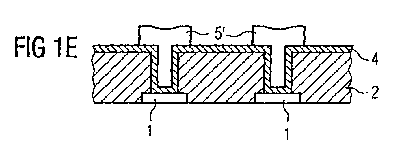
Die Erfindung betrifft ein Verfahren zur Herstellung einer
Verdrahtung für Kontaktlöcher, wobei zum Ausbilden einer Al-GeCu-haltigen
zweiten Verdrahtungsschicht (5) an der Oberfläche
einer Isolationsschicht (2) ein Niedertemperatur-PVD-Verfahren
zum Auffüllen von Kontaktlöchern (3) verwendet
wird. Auf Grund der dabei ausgebildeten relativ kleinen Korngrößen
und Ausscheidungen kann diese Schicht in einem nachfolgenden
Strukturierungsschritt unmittelbar strukturiert
werden, wodurch man eine äußerst zuverlässige Verdrahtung auf
kostengünstige Art und Weise mit einfacher Integrierbarkeit
in bestehende Prozess-Abläufe erhält.
Applications Claiming Priority (2)
| Application Number | Priority Date | Filing Date | Title |
|---|---|---|---|
| DE10032792A DE10032792A1 (en) | 2000-06-28 | 2000-06-28 | Method of making via hole wiring |
| DE10032792 | 2000-06-28 |
Publications (2)
| Publication Number | Publication Date |
|---|---|
| EP1168431A2 EP1168431A2 (en) | 2002-01-02 |
| EP1168431A3 true EP1168431A3 (en) | 2003-05-07 |
Family
ID=7647954
Family Applications (1)
| Application Number | Title | Priority Date | Filing Date |
|---|---|---|---|
| EP01115187A Withdrawn EP1168431A3 (en) | 2000-06-28 | 2001-06-22 | Process for the manufacture of a wiring for contact holes |
Country Status (4)
| Country | Link |
|---|---|
| US (1) | US6602788B2 (en) |
| EP (1) | EP1168431A3 (en) |
| DE (1) | DE10032792A1 (en) |
| TW (1) | TW515043B (en) |
Families Citing this family (5)
| Publication number | Priority date | Publication date | Assignee | Title |
|---|---|---|---|---|
| US6815340B1 (en) * | 2002-05-15 | 2004-11-09 | Advanced Micro Devices, Inc. | Method of forming an electroless nucleation layer on a via bottom |
| US20070032060A1 (en) * | 2005-08-05 | 2007-02-08 | Ta-Hung Yang | Method for forming conductive wiring and interconnects |
| KR20080054042A (en) * | 2006-12-12 | 2008-06-17 | 동부일렉트로닉스 주식회사 | Method of manufacturing metal pattern of semiconductor device |
| US20090221144A1 (en) * | 2008-03-03 | 2009-09-03 | National Applied Research Laboratories | Manufacturing method for nano scale Ge metal structure |
| US11101130B2 (en) * | 2018-12-27 | 2021-08-24 | Raytheon Company | Method of filling grooves and holes in a substrate |
Citations (4)
| Publication number | Priority date | Publication date | Assignee | Title |
|---|---|---|---|---|
| US5776827A (en) * | 1993-08-27 | 1998-07-07 | Yamaha Corporation | Wiring-forming method |
| US5789317A (en) * | 1996-04-12 | 1998-08-04 | Micron Technology, Inc. | Low temperature reflow method for filling high aspect ratio contacts |
| US5856026A (en) * | 1994-08-05 | 1999-01-05 | International Business Machines Corporation | High aspect ratio low resistivity lines/vias by surface diffusion |
| US6110829A (en) * | 1997-10-23 | 2000-08-29 | Advanced Micro Devices, Inc. | Ultra-low temperature Al fill for sub-0.25 μm generation of ICs using an Al-Ge-Cu alloy |
Family Cites Families (7)
| Publication number | Priority date | Publication date | Assignee | Title |
|---|---|---|---|---|
| US4970176A (en) * | 1989-09-29 | 1990-11-13 | Motorola, Inc. | Multiple step metallization process |
| JPH04209572A (en) * | 1990-12-07 | 1992-07-30 | Nec Corp | Semiconductor device |
| US5358616A (en) * | 1993-02-17 | 1994-10-25 | Ward Michael G | Filling of vias and contacts employing an aluminum-germanium alloy |
| US5691571A (en) * | 1994-12-28 | 1997-11-25 | Nec Corporation | Semiconductor device having fine contact hole with high aspect ratio |
| US6225218B1 (en) * | 1995-12-20 | 2001-05-01 | Semiconductor Energy Laboratory Co., Ltd. | Semiconductor device and its manufacturing method |
| DE69736717T2 (en) * | 1996-12-12 | 2007-09-13 | Asahi Kasei Kabushiki Kaisha | METHOD FOR PRODUCING A SEMICONDUCTOR DEVICE |
| US5980657A (en) * | 1998-03-10 | 1999-11-09 | Micron Technology, Inc. | Alloy for enhanced filling of high aspect ratio dual damascene structures |
-
2000
- 2000-06-28 DE DE10032792A patent/DE10032792A1/en not_active Withdrawn
-
2001
- 2001-06-22 EP EP01115187A patent/EP1168431A3/en not_active Withdrawn
- 2001-06-27 TW TW090115546A patent/TW515043B/en not_active IP Right Cessation
- 2001-06-28 US US09/894,942 patent/US6602788B2/en not_active Expired - Fee Related
Patent Citations (4)
| Publication number | Priority date | Publication date | Assignee | Title |
|---|---|---|---|---|
| US5776827A (en) * | 1993-08-27 | 1998-07-07 | Yamaha Corporation | Wiring-forming method |
| US5856026A (en) * | 1994-08-05 | 1999-01-05 | International Business Machines Corporation | High aspect ratio low resistivity lines/vias by surface diffusion |
| US5789317A (en) * | 1996-04-12 | 1998-08-04 | Micron Technology, Inc. | Low temperature reflow method for filling high aspect ratio contacts |
| US6110829A (en) * | 1997-10-23 | 2000-08-29 | Advanced Micro Devices, Inc. | Ultra-low temperature Al fill for sub-0.25 μm generation of ICs using an Al-Ge-Cu alloy |
Non-Patent Citations (1)
| Title |
|---|
| KIKUTA K ET AL: "ALUMINUM-GERMANIUM-COPPER MULTILEVEL DAMASCENE PROCESS USING LOW-TEMPERATURE REFLOW SPUTTERING AND CHEMICAL MECHANICAL POLISHING", IEEE TRANSACTIONS ON ELECTRON DEVICES, IEEE INC. NEW YORK, US, VOL. 43, NR. 5, PAGE(S) 739-744, ISSN: 0018-9383, XP000596269 * |
Also Published As
| Publication number | Publication date |
|---|---|
| TW515043B (en) | 2002-12-21 |
| US6602788B2 (en) | 2003-08-05 |
| EP1168431A2 (en) | 2002-01-02 |
| DE10032792A1 (en) | 2002-01-17 |
| US20020006720A1 (en) | 2002-01-17 |
Similar Documents
| Publication | Publication Date | Title |
|---|---|---|
| EP0973050A3 (en) | Method for manufacturing planar waveguide structures and waveguide structure | |
| ATE320915T1 (en) | SURFACE TREATED ELECTRICALLY CONDUCTIVE METAL PART AND METHOD FOR PRODUCING THE SAME | |
| EP1182699A3 (en) | Process for forming a thick dielectric region in a semiconductor substrate | |
| EP1091420A3 (en) | Method for the production of contact structures in solar cells | |
| EP0987754A3 (en) | Method of producing a trench capacitor with insulation collar | |
| EP1239266A3 (en) | Process for manufacturing a sensorhousing, sensor and the use thereof | |
| DE19713014A1 (en) | Quartz glass component for use in semiconductor manufacturing | |
| EP1128428A3 (en) | Method of manufacturing a semiconductor device | |
| EP0981155A3 (en) | Method for manufacturing a semiconductor isolation layer and semiconductor device comprising said semiconductor isolation layer | |
| EP1584708A3 (en) | Process for the treatment of laser-structured plastic surfaces | |
| EP1168431A3 (en) | Process for the manufacture of a wiring for contact holes | |
| DE102004017411A1 (en) | In situ metal barrier deposition for sputter etching on a connection structure | |
| EP0865081A3 (en) | Process for fabricating electronic elements | |
| EP1168443A3 (en) | Process for the manufacture of a dielectric antifuse structure | |
| DE2621139A1 (en) | INTEGRATED CIRCUIT AND METHOD FOR MANUFACTURING IT | |
| EP1536466A3 (en) | Carrier substrate for semiconductor multilayer strcuture and method of manufacturing semiconductor chips | |
| EP1107322A3 (en) | High-temperature superconductor device and manufacturing method | |
| EP1275520A3 (en) | Process of production of a flexible rubber blanket sleeve | |
| EP0889506A3 (en) | Etching process | |
| EP1049191A3 (en) | Procedure for the production of electronical elements with strip lines | |
| EP1193742A3 (en) | Method for fabricating integrated circuits, corresponding circuits, particularly tunnel contacts | |
| EP1453155A3 (en) | Method for producing slip ring brushes and such a produced slip ring brush | |
| DE10345460A1 (en) | A method of making a hole trench storage capacitor in a semiconductor substrate and hole trench storage capacitor | |
| EP1360143B1 (en) | Method for producing surface micromechanical structures, and sensor | |
| EP0993029A3 (en) | Process for the fabrication of crystalline semiconductor layers |
Legal Events
| Date | Code | Title | Description |
|---|---|---|---|
| PUAI | Public reference made under article 153(3) epc to a published international application that has entered the european phase |
Free format text: ORIGINAL CODE: 0009012 |
|
| 17P | Request for examination filed |
Effective date: 20010622 |
|
| AK | Designated contracting states |
Kind code of ref document: A2 Designated state(s): AT BE CH CY DE DK ES FI FR GB GR IE IT LI LU MC NL PT SE TR |
|
| AX | Request for extension of the european patent |
Free format text: AL;LT;LV;MK;RO;SI |
|
| PUAL | Search report despatched |
Free format text: ORIGINAL CODE: 0009013 |
|
| AK | Designated contracting states |
Designated state(s): AT BE CH CY DE DK ES FI FR GB GR IE IT LI LU MC NL PT SE TR |
|
| AX | Request for extension of the european patent |
Extension state: AL LT LV MK RO SI |
|
| 17Q | First examination report despatched |
Effective date: 20030923 |
|
| AKX | Designation fees paid |
Designated state(s): DE FR GB IE IT |
|
| GRAP | Despatch of communication of intention to grant a patent |
Free format text: ORIGINAL CODE: EPIDOSNIGR1 |
|
| STAA | Information on the status of an ep patent application or granted ep patent |
Free format text: STATUS: THE APPLICATION IS DEEMED TO BE WITHDRAWN |
|
| 18D | Application deemed to be withdrawn |
Effective date: 20091006 |