EP1168040A2 - Optical modulation system - Google Patents
Optical modulation system Download PDFInfo
- Publication number
- EP1168040A2 EP1168040A2 EP01303047A EP01303047A EP1168040A2 EP 1168040 A2 EP1168040 A2 EP 1168040A2 EP 01303047 A EP01303047 A EP 01303047A EP 01303047 A EP01303047 A EP 01303047A EP 1168040 A2 EP1168040 A2 EP 1168040A2
- Authority
- EP
- European Patent Office
- Prior art keywords
- light
- combined signals
- optical modulation
- predetermined frequency
- electrical signal
- Prior art date
- Legal status (The legal status is an assumption and is not a legal conclusion. Google has not performed a legal analysis and makes no representation as to the accuracy of the status listed.)
- Granted
Links
- 230000003287 optical effect Effects 0.000 title claims abstract description 81
- 238000010586 diagram Methods 0.000 description 8
- 239000000835 fiber Substances 0.000 description 5
- 238000004891 communication Methods 0.000 description 3
- 230000003247 decreasing effect Effects 0.000 description 3
- 230000000694 effects Effects 0.000 description 3
- 239000006185 dispersion Substances 0.000 description 2
- 238000000034 method Methods 0.000 description 2
- 239000004065 semiconductor Substances 0.000 description 2
- 238000001228 spectrum Methods 0.000 description 2
- 229910003327 LiNbO3 Inorganic materials 0.000 description 1
- 229910012463 LiTaO3 Inorganic materials 0.000 description 1
- 238000010521 absorption reaction Methods 0.000 description 1
- 239000013078 crystal Substances 0.000 description 1
- 238000005516 engineering process Methods 0.000 description 1
- 238000004519 manufacturing process Methods 0.000 description 1
- 230000009022 nonlinear effect Effects 0.000 description 1
- 238000000926 separation method Methods 0.000 description 1
- 230000003595 spectral effect Effects 0.000 description 1
Images


Classifications
-
- G—PHYSICS
- G02—OPTICS
- G02F—OPTICAL DEVICES OR ARRANGEMENTS FOR THE CONTROL OF LIGHT BY MODIFICATION OF THE OPTICAL PROPERTIES OF THE MEDIA OF THE ELEMENTS INVOLVED THEREIN; NON-LINEAR OPTICS; FREQUENCY-CHANGING OF LIGHT; OPTICAL LOGIC ELEMENTS; OPTICAL ANALOGUE/DIGITAL CONVERTERS
- G02F1/00—Devices or arrangements for the control of the intensity, colour, phase, polarisation or direction of light arriving from an independent light source, e.g. switching, gating or modulating; Non-linear optics
- G02F1/01—Devices or arrangements for the control of the intensity, colour, phase, polarisation or direction of light arriving from an independent light source, e.g. switching, gating or modulating; Non-linear optics for the control of the intensity, phase, polarisation or colour
- G02F1/03—Devices or arrangements for the control of the intensity, colour, phase, polarisation or direction of light arriving from an independent light source, e.g. switching, gating or modulating; Non-linear optics for the control of the intensity, phase, polarisation or colour based on ceramics or electro-optical crystals, e.g. exhibiting Pockels effect or Kerr effect
- G02F1/0305—Constructional arrangements
- G02F1/0311—Structural association of optical elements, e.g. lenses, polarizers, phase plates, with the crystal
-
- G—PHYSICS
- G02—OPTICS
- G02F—OPTICAL DEVICES OR ARRANGEMENTS FOR THE CONTROL OF LIGHT BY MODIFICATION OF THE OPTICAL PROPERTIES OF THE MEDIA OF THE ELEMENTS INVOLVED THEREIN; NON-LINEAR OPTICS; FREQUENCY-CHANGING OF LIGHT; OPTICAL LOGIC ELEMENTS; OPTICAL ANALOGUE/DIGITAL CONVERTERS
- G02F1/00—Devices or arrangements for the control of the intensity, colour, phase, polarisation or direction of light arriving from an independent light source, e.g. switching, gating or modulating; Non-linear optics
- G02F1/01—Devices or arrangements for the control of the intensity, colour, phase, polarisation or direction of light arriving from an independent light source, e.g. switching, gating or modulating; Non-linear optics for the control of the intensity, phase, polarisation or colour
- G02F1/03—Devices or arrangements for the control of the intensity, colour, phase, polarisation or direction of light arriving from an independent light source, e.g. switching, gating or modulating; Non-linear optics for the control of the intensity, phase, polarisation or colour based on ceramics or electro-optical crystals, e.g. exhibiting Pockels effect or Kerr effect
- G02F1/0327—Operation of the cell; Circuit arrangements
-
- G—PHYSICS
- G02—OPTICS
- G02F—OPTICAL DEVICES OR ARRANGEMENTS FOR THE CONTROL OF LIGHT BY MODIFICATION OF THE OPTICAL PROPERTIES OF THE MEDIA OF THE ELEMENTS INVOLVED THEREIN; NON-LINEAR OPTICS; FREQUENCY-CHANGING OF LIGHT; OPTICAL LOGIC ELEMENTS; OPTICAL ANALOGUE/DIGITAL CONVERTERS
- G02F2/00—Demodulating light; Transferring the modulation of modulated light; Frequency-changing of light
- G02F2/02—Frequency-changing of light, e.g. by quantum counters
-
- G—PHYSICS
- G02—OPTICS
- G02F—OPTICAL DEVICES OR ARRANGEMENTS FOR THE CONTROL OF LIGHT BY MODIFICATION OF THE OPTICAL PROPERTIES OF THE MEDIA OF THE ELEMENTS INVOLVED THEREIN; NON-LINEAR OPTICS; FREQUENCY-CHANGING OF LIGHT; OPTICAL LOGIC ELEMENTS; OPTICAL ANALOGUE/DIGITAL CONVERTERS
- G02F2201/00—Constructional arrangements not provided for in groups G02F1/00 - G02F7/00
- G02F2201/17—Multi-pass arrangements, i.e. arrangements to pass light a plurality of times through the same element, e.g. by using an enhancement cavity
-
- G—PHYSICS
- G02—OPTICS
- G02F—OPTICAL DEVICES OR ARRANGEMENTS FOR THE CONTROL OF LIGHT BY MODIFICATION OF THE OPTICAL PROPERTIES OF THE MEDIA OF THE ELEMENTS INVOLVED THEREIN; NON-LINEAR OPTICS; FREQUENCY-CHANGING OF LIGHT; OPTICAL LOGIC ELEMENTS; OPTICAL ANALOGUE/DIGITAL CONVERTERS
- G02F2203/00—Function characteristic
- G02F2203/05—Function characteristic wavelength dependent
- G02F2203/055—Function characteristic wavelength dependent wavelength filtering
Definitions
- the present invention relates to a system that uses high-frequency signals to modulate optical signals, and particularly to a reciprocating optical modulation system that can generate an optical signal having a frequency that is a number of times higher than that of the applied electrical signal.
- Optical modulation by high-frequency signals is generally accomplished by inputting an optical carrier wave and a high-frequency electrical signal to an optical modulator and performing intensity modulation or phase modulation or other such modulation.
- the high-frequency electrical signal is multiplied to form an even higher-frequency signal that is used for the optical modulation.
- the maximum modulation frequency is determined by the upper limit of the electrical signal.
- an electrical signal that is multiplied or amplified or other such signal is limited by the maximum characteristic of the electrical circuit. There is therefore a need to overcome this drawback.
- phase-modulation configuration that uses a high modulation index
- a stripline resonator is used as the modulator electrodes, making it difficult to change the modulation frequency.
- the amplifier would place an upper limit on the high-frequency electrical signal.
- an object of the present invention is to provide a reciprocating optical modulation system that can readily generate high-order sidebands even with a high-frequency electrical signal having a smaller amplitude than that of the prior art phase modulation configuration described above that uses high modulation-index setting.
- the present invention provides a reciprocating optical modulation system, the system comprising: means that, taking n as a predetermined integer of 1 or more, modulates light of a predetermined frequency to produce an nth order sideband group thereof; means that modulates the nth order sideband group to produce an (n+1)th order sideband group; and means that selects at least part of the (n+1)th order sideband group.
- “(n+1)th order sideband” refers to a sideband (n+1)-times the modulation frequency that is frequency-separated from the carrier wave
- the "(n+1)th order sideband group” refers to two sidebands located symmetrically with respect to the carrier wave.
- the reciprocating optical modulation system of the present invention also includes a light path that is shortened by being folded by a reflection means.
- the system also includes a plurality of modulation means, to which at least one of sideband groups of a different order is input, a configuration that can reduce the cost of the system by decreasing the number of modulators used.
- the present invention also provides a reciprocating optical modulation system comprising first reflection means that prior to modulation passes light of the predetermined frequency and reflects light of other frequencies; and second reflection means that with respect to the predetermined integer n of 1 or more, passes (n+1)th sidebands and reflects other light
- a reciprocating optical modulation system comprising first reflection means that prior to modulation passes light of the predetermined frequency and reflects light of other frequencies; and second reflection means that with respect to the predetermined integer n of 1 or more, passes (n+1)th sidebands and reflects other light
- One example of the system configuration comprises a laser light source, the first reflection means comprised of a narrow-bandpass filter, an optical modulator, and the second reflection means comprised of a band-limiting filter.
- This reciprocating optical modulation system can further includes a laser light source and an optical modulator, wherein the first reflection means is comprised of a narrow-bandpass filter, and the second reflection means is comprised of a band-limiting filter.
- the invention also provides a reciprocating optical modulation system that further includes means for converting part of the optical output into electrical signals, and means for re-inputting the electrical signals to the modulation signal of the phase modulator.
- the system also includes means that uses a nonlinear element for combining a portion of the light input to the system with sideband output from the system, and means for extracting from the mixed signals electrical signals of a predetermined frequency band.
- the light that is input has a frequency f 0 .
- a narrow-bandpass filter 1 passes this input light of frequency f 0 , but reflects light having a frequency that deviates even slightly from that frequency.
- the narrow-bandpass filter 1 is therefore used as a reflection means.
- An intensity modulator 2 can modulate left or right oriented light with a modulation frequency fm.
- a band-limiting filter 3 reflects light of up to n order sideband frequency, for example up to third order, and passes other light. Therefore, the band-limiting filter 3, too, is used as a reflection means.
- the carrier wave portion of the light passes through the narrow-bandpass filter 1, leaving just the sideband depicted in Figure 2(d), which is reflected and further modulated, resulting in the spectrum of Figure 2(e).
- this modulation process produces first-order and third-order sidebands.
- the third-order sideband, shown in Figure 2(g) passes through the band-limiting filter 3, while the first-order sideband shown in Figure 2(f) is reflected thereby. In this way, the third-order sideband is output from the band-limiting filter 3.
- Modulators that can be used for the purposes of the present invention include resonance type modulators and traveling wave type modulators.
- a traveling wave modulator has electrodes at both ends, meaning that a modulation signal can be input from either end, enabling the same modulation to be imparted to the light whichever way the light is traveling.
- FIG 3 is a block diagram showing a variation of the system configuration shown in Figure 1. Specifically, a phase modulator 2b has been added to the system of Figure 1.
- the optical output can be intensity-modulated by supplying the phase modulator 2b with an additional modulation signal.
- the phase modulator 2b can be made to perform amplitude modulation by a change in the interference conditions effected by changing the phase of the light reflected in an optical resonator comprising the narrow-bandpass filter 1 and the band-limiting filter 3.
- FIG 4 is a block diagram of a modulation system configuration used to verify the principle of the present invention.
- Reflection by a fiber grating (FBG) 7 and a fiber grating (FBG) 8 causes the light input to be passed through the phase modulator 2b a plurality of times, generating a high-order sideband.
- a laser light source 5 is a 10-milliwatt semiconductor laser that operates at a wavelength of 1550 nanometers.
- An isolator 6 is of a commercially available type manufactured by Newport Company.
- the fiber gratings 7 and 8 are also of a commercially available type, made by M Company. This type of the fiber gratings is described, for example, in "Trends in the Development of Fiber Grating Technology," by S.
- the modulator 2 is a commercially available traveling wave type phase modulator manufactured by Sumitomo Osaka Cement Co., Ltd., that can handle high-frequency electrical signal inputs having a frequency of up to 40 GHz. With a modulation system thus configured, it was possible to obtain a -32 dBm sideband with a carrier frequency separation of 210 GHz, from the input of a 30 GHz, 27.8 dBm modulation signal.
- FIG. 5 shows the arrangement of a first embodiment of the modulation system of the present invention.
- This modulation system is provided with an isolator 6 to suppress the effect of light returning back from the narrow-bandpass filter 1, a dispersion compensator 10 for preventing the efficiency of the reciprocating modulation from decreasing even at high-order sideband frequencies, and an optical amplifier 9 for obtaining a high output.
- the compensator 10 compensates for dispersion arising in the other components. It is possible to dispense with the compensator 10 by equipping the other system components with this function.
- the intensity of the optical output generally fluctuates.
- the output can be kept stable by, for example, using a photodiode in a photodetector/amplifier 11 to convert the optical output to an electrical signal that is fed back to the phase modulator 2b.
- a modulator can be used that attenuates the carrier wave, leaving both sidebands, such as the modulator described in "Optical Subcarrier Generation Using Integrated LN Phase Modulator," by Shimozu, et al., C-3-20, 2000 General Meeting of The Institute of Electronics, Information and Communication Engineers, p. 199.
- a semiconductor-based absorption modulator, a Mach-Zehender interference type intensity modulator or an electro-optic-effect phase modulator can be used for the modulator 2.
- Modulation index can be readily improved by using resonance type intensity and phase modulators that perform the modulation by using electrodes that resonate at the modulation frequency. As can be readily understood, this means that sufficient modulation can be obtained using just a small amount of high-frequency power.
- the properties of a resonance type modulator are described in "60 GHz Band Resonance Type LiNbO 3 Optical Modulator," by Sasaki, et al., C-3-125, 2000 General Meeting of The Institute of Electronics, Information and Communication Engineers, p. 279.
- supplying another modulation signal to the phase modulator 2b enables intensity-modulation of the optical output.
- the intensity of the optical output generally fluctuates, it can be kept stable by, for example, using a photodiode in the photodetector/amplifier 11 to convert the optical output to an electrical signal that is used as feedback to the phase modulator.
- Figure 6 is a simplified representation of a second embodiment of the modulation system of the invention.
- light emitted by a laser light source 5 is modulated by a reciprocating optical modulator 4, which has optical filter properties, producing double sidebands having frequencies equivalent to n times the modulation frequency fm (where n is a predetermined positive integer 1, 3, 5...), which are applied to a photodetector 12.
- the photodetector 12 is a nonlinear element, and the result of this nonlinearity is an electrical signal having a frequency that is n times the frequency differential of the two sidebands, i.e. 2 x fm.
- FIG. 7 shows a simplified representation of a third embodiment of the modulation system of this invention.
- light from a laser light source 5 is modulated by a reciprocating optical modulator 4, which has optical filter properties, producing a sideband having a frequency equivalent to n times the modulation frequency (where n is a predetermined positive integer 1, 3, 5).
- This sideband signal and light from the laser light source 5 are applied to a photodetector 12. Owing to the nonlinear effect of the photodetector 12, this gives rise to an electrical signal having a frequency that is the frequency differential between the sideband and the light from the laser light source 5.
- a filter 13 is used to select a signal of a predetermined frequency.
- the modulation system of the present invention comprises means that, taking n as a predetermined integer of 1 or more, modulates light of a predetermined frequency to produce a group of nth order sidebands thereof; means for modulating the nth order sideband group to produce an (n+1)th order sideband group; and means for selecting at least part of the (n+1)th order sideband group.
- the system also includes a configuration in which reflection means are used to fold the light path, making it possible to configure the system with a short light path.
- the system also includes a configuration with a plurality of modulation means, at least one of which receives the input of a group of sidebands of different orders, which makes it possible to reduce the manufacturing cost by decreasing the number of modulators used.
- the modulation system includes first and second reflection means, with the first reflection means transmitting pre-modulation light of the predetermined frequency and reflecting light of other frequencies; and the second reflection means, with respect to the predetermined integer n of 1 or more, transmitting (n+1)th sidebands and reflecting other light.
- the system can be configured with a laser light source, the first reflection means comprising a narrow-bandpass filter, an optical modulator, and the second reflection means comprising a band-limiting filter, reducing the cost.
- the first reflection means comprises, a narrow-bandpass filter, and the second reflection means comprises an optical modulator, facilitates the modulation of optical signals.
- the reciprocating optical modulation system also includes one having means for converting part of the optical output into electrical signals, and means for re-applying the electrical signals to the modulation signal of the phase modulator, which makes it possible to readily obtain a stable optical signal.
- the system also includes means that uses a nonlinear element for combining a portion of the light input to the system with sideband signals output from the system, and means for extracting electrical signals of a predetermined frequency band from the signals thus combined.
Landscapes
- Physics & Mathematics (AREA)
- Nonlinear Science (AREA)
- General Physics & Mathematics (AREA)
- Optics & Photonics (AREA)
- Chemical & Material Sciences (AREA)
- Engineering & Computer Science (AREA)
- Ceramic Engineering (AREA)
- Crystallography & Structural Chemistry (AREA)
- Optical Modulation, Optical Deflection, Nonlinear Optics, Optical Demodulation, Optical Logic Elements (AREA)
- Optical Communication System (AREA)
Abstract
Description
- The present invention relates to a system that uses high-frequency signals to modulate optical signals, and particularly to a reciprocating optical modulation system that can generate an optical signal having a frequency that is a number of times higher than that of the applied electrical signal.
- Optical modulation by high-frequency signals is generally accomplished by inputting an optical carrier wave and a high-frequency electrical signal to an optical modulator and performing intensity modulation or phase modulation or other such modulation. In the case of this method, in order to obtain a sideband having a frequency that is at least as high as that of the applied high-frequency electrical signal, the high-frequency electrical signal is multiplied to form an even higher-frequency signal that is used for the optical modulation. However, even when the high-frequency electrical signal is thus multiplied, the maximum modulation frequency is determined by the upper limit of the electrical signal. Thus, in terms of frequency, an electrical signal that is multiplied or amplified or other such signal is limited by the maximum characteristic of the electrical circuit. There is therefore a need to overcome this drawback.
- There have been reports of attempts to produce a sideband with a frequency higher than that of the applied high-frequency signal, using phase modulation with a high modulation index. One reference ("Generation of Ultrashort Optical Pulses Using Domain-Inverted External Phase Modulator," by T. Kobayashi, OYO BUTURI, voL 67 No. 9 (1998), pp. 1056-1060) describes applying a 16.26 GHz electrical signal to an optical modulator having a waveguide formed of an electro-optical crystal of LiTaO3 on which a stripline resonator was disposed. With a modulation index set at 87 radial, the spectral bandwidth was around 2.9 THz.
- However, with the above type of phase-modulation configuration that uses a high modulation index, in order to increase the amplitude of the high-frequency electrical signal so as to obtain the high modulation index, a stripline resonator is used as the modulator electrodes, making it difficult to change the modulation frequency. Although it is easy to think of a configuration in which using a resonator as the modulator electrodes can be avoided by amplifying the electrical signal, thereby making it possible to readily change the modulation frequency, it is well known that the amplifier would place an upper limit on the high-frequency electrical signal.
- In view of the above, an object of the present invention is to provide a reciprocating optical modulation system that can readily generate high-order sidebands even with a high-frequency electrical signal having a smaller amplitude than that of the prior art phase modulation configuration described above that uses high modulation-index setting.
- To attain the above object, the present invention provides a reciprocating optical modulation system, the system comprising: means that, taking n as a predetermined integer of 1 or more, modulates light of a predetermined frequency to produce an nth order sideband group thereof; means that modulates the nth order sideband group to produce an (n+1)th order sideband group; and means that selects at least part of the (n+1)th order sideband group. Here, "(n+1)th order sideband" refers to a sideband (n+1)-times the modulation frequency that is frequency-separated from the carrier wave, and the "(n+1)th order sideband group" refers to two sidebands located symmetrically with respect to the carrier wave.
- The reciprocating optical modulation system of the present invention also includes a light path that is shortened by being folded by a reflection means. The system also includes a plurality of modulation means, to which at least one of sideband groups of a different order is input, a configuration that can reduce the cost of the system by decreasing the number of modulators used.
- The present invention also provides a reciprocating optical modulation system comprising first reflection means that prior to modulation passes light of the predetermined frequency and reflects light of other frequencies; and second reflection means that with respect to the predetermined integer n of 1 or more, passes (n+1)th sidebands and reflects other light One example of the system configuration comprises a laser light source, the first reflection means comprised of a narrow-bandpass filter, an optical modulator, and the second reflection means comprised of a band-limiting filter. This reciprocating optical modulation system can further includes a laser light source and an optical modulator, wherein the first reflection means is comprised of a narrow-bandpass filter, and the second reflection means is comprised of a band-limiting filter. The reciprocating optical modulation system can further includes a phase modulator, wherein the first reflection means is comprised of a narrow-bandpass filter, and the second reflection means is comprised of a band-limiting filter.
- The invention also provides a reciprocating optical modulation system that further includes means for converting part of the optical output into electrical signals, and means for re-inputting the electrical signals to the modulation signal of the phase modulator. In another example, the system also includes means that uses a nonlinear element for combining a portion of the light input to the system with sideband output from the system, and means for extracting from the mixed signals electrical signals of a predetermined frequency band.
- Further features of the invention, its nature and various advantages will be more apparent from the accompanying drawings and following detailed description of the invention, in which:-
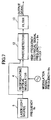
- Figure 1 is a block diagram of the basic configuration of a reciprocating optical modulation system of the present invention,
- Figures 2(a) to 2(g) are drawings for explaining what happens up until light of frequency f0 is modulated and the third order sideband signal is output,
- Figure 3 is a block diagram showing a variation in the basic system configuration shown in Figure 1,
- Figure 4 is a block diagram of a modulator system used to verify the principle of the present invention,
- Figure 5 is a block diagram of a first embodiment of the reciprocating optical modulation system of the invention,
- Figure 6 is a block diagram of a second embodiment of the reciprocating optical modulation system of the invention, and
- Figure 7 is a block diagram of a third embodiment of the reciprocating optical modulation system of the invention.
-
- The invention will now be described with reference to the accompanying drawings. In Figure 1, the light that is input has a frequency f0. A narrow-
bandpass filter 1 passes this input light of frequency f0, but reflects light having a frequency that deviates even slightly from that frequency. The narrow-bandpass filter 1 is therefore used as a reflection means. Anintensity modulator 2 can modulate left or right oriented light with a modulation frequency fm. A band-limitingfilter 3 reflects light of up to n order sideband frequency, for example up to third order, and passes other light. Therefore, the band-limitingfilter 3, too, is used as a reflection means. - With the configuration described above, light of frequency f0 that is input after passing through the narrow-
bandpass filter 1 is modulated, resulting in the sideband of Figure 2(b). For simplicity, it is assumed that the modulation is linear and that only first-order sidebands are generated on each side. In Figure 2, solid lines are used to denote sidebands generated by modulation, while dotted lines denote the wavelength position of the light prior to the modulation. The band-limitingfilter 3 reflects the modulated light back through theintensity modulator 2. This subjects the sidebands to modulation, creating the spectrum of Figure 2(c). The carrier wave portion of the light passes through the narrow-bandpass filter 1, leaving just the sideband depicted in Figure 2(d), which is reflected and further modulated, resulting in the spectrum of Figure 2(e). Thus, this modulation process produces first-order and third-order sidebands. The third-order sideband, shown in Figure 2(g), passes through the band-limitingfilter 3, while the first-order sideband shown in Figure 2(f) is reflected thereby. In this way, the third-order sideband is output from the band-limitingfilter 3. - The above description has been made with reference to the
intensity modulator 2. However, the same effect is also obtained with a phase modulator. Modulators that can be used for the purposes of the present invention include resonance type modulators and traveling wave type modulators. A traveling wave modulator has electrodes at both ends, meaning that a modulation signal can be input from either end, enabling the same modulation to be imparted to the light whichever way the light is traveling. - Figure 3 is a block diagram showing a variation of the system configuration shown in Figure 1. Specifically, a
phase modulator 2b has been added to the system of Figure 1. The optical output can be intensity-modulated by supplying thephase modulator 2b with an additional modulation signal. Thephase modulator 2b can be made to perform amplitude modulation by a change in the interference conditions effected by changing the phase of the light reflected in an optical resonator comprising the narrow-bandpass filter 1 and the band-limitingfilter 3. - Figure 4 is a block diagram of a modulation system configuration used to verify the principle of the present invention. Reflection by a fiber grating (FBG) 7 and a fiber grating (FBG) 8 causes the light input to be passed through the
phase modulator 2b a plurality of times, generating a high-order sideband. Alaser light source 5 is a 10-milliwatt semiconductor laser that operates at a wavelength of 1550 nanometers. Anisolator 6 is of a commercially available type manufactured by Newport Company. Thefiber gratings 7 and 8 are also of a commercially available type, made by M Company. This type of the fiber gratings is described, for example, in "Trends in the Development of Fiber Grating Technology," by S. Inoue, C-3-67, 2000 General Meeting of The Institute of Electronics, Information and Communication Engineers, pp. 246-247. Themodulator 2 is a commercially available traveling wave type phase modulator manufactured by Sumitomo Osaka Cement Co., Ltd., that can handle high-frequency electrical signal inputs having a frequency of up to 40 GHz. With a modulation system thus configured, it was possible to obtain a -32 dBm sideband with a carrier frequency separation of 210 GHz, from the input of a 30 GHz, 27.8 dBm modulation signal. - Figure 5 shows the arrangement of a first embodiment of the modulation system of the present invention. This modulation system is provided with an
isolator 6 to suppress the effect of light returning back from the narrow-bandpass filter 1, adispersion compensator 10 for preventing the efficiency of the reciprocating modulation from decreasing even at high-order sideband frequencies, and anoptical amplifier 9 for obtaining a high output. Thecompensator 10 compensates for dispersion arising in the other components. It is possible to dispense with thecompensator 10 by equipping the other system components with this function. - The intensity of the optical output generally fluctuates. However, the output can be kept stable by, for example, using a photodiode in a photodetector/
amplifier 11 to convert the optical output to an electrical signal that is fed back to thephase modulator 2b. This is because the fluctuations in the intensity of the optical output are caused by variations in the phase of the light arising from variations in the light path. Instead of thephase modulator 2b, a modulator can be used that attenuates the carrier wave, leaving both sidebands, such as the modulator described in "Optical Subcarrier Generation Using Integrated LN Phase Modulator," by Shimozu, et al., C-3-20, 2000 General Meeting of The Institute of Electronics, Information and Communication Engineers, p. 199. A semiconductor-based absorption modulator, a Mach-Zehender interference type intensity modulator or an electro-optic-effect phase modulator can be used for themodulator 2. - Modulation index can be readily improved by using resonance type intensity and phase modulators that perform the modulation by using electrodes that resonate at the modulation frequency. As can be readily understood, this means that sufficient modulation can be obtained using just a small amount of high-frequency power. The properties of a resonance type modulator are described in "60 GHz Band Resonance Type LiNbO3 Optical Modulator," by Sasaki, et al., C-3-125, 2000 General Meeting of The Institute of Electronics, Information and Communication Engineers, p. 279.
- In the above-described modulator, as long as the
optical amplifier 9 is between the narrow-bandpass filter 1 and the band-limitingfilter 3, the precise position has no particular significance. Similarly, there is no particular significance attached to the order in which themodulator 2,optical amplifier 9,compensator 10 andphase modulator 2b are arranged, because the same effect is obtainable even if a different order is used. - As mentioned above, supplying another modulation signal to the
phase modulator 2b enables intensity-modulation of the optical output. As has also been described above, while the intensity of the optical output generally fluctuates, it can be kept stable by, for example, using a photodiode in the photodetector/amplifier 11 to convert the optical output to an electrical signal that is used as feedback to the phase modulator. - Next, an example of harmonic generation using the reciprocating optical modulation system of the present invention will be described. Figure 6 is a simplified representation of a second embodiment of the modulation system of the invention. In Figure 6, light emitted by a
laser light source 5 is modulated by a reciprocatingoptical modulator 4, which has optical filter properties, producing double sidebands having frequencies equivalent to n times the modulation frequency fm (where n is a predeterminedpositive integer photodetector 12. Thephotodetector 12 is a nonlinear element, and the result of this nonlinearity is an electrical signal having a frequency that is n times the frequency differential of the two sidebands, i.e. 2 x fm. - Figure 7 shows a simplified representation of a third embodiment of the modulation system of this invention. With respect to Figure 7, light from a
laser light source 5 is modulated by a reciprocatingoptical modulator 4, which has optical filter properties, producing a sideband having a frequency equivalent to n times the modulation frequency (where n is a predeterminedpositive integer laser light source 5 are applied to aphotodetector 12. Owing to the nonlinear effect of thephotodetector 12, this gives rise to an electrical signal having a frequency that is the frequency differential between the sideband and the light from thelaser light source 5. Afilter 13 is used to select a signal of a predetermined frequency. Again, it can readily be understood that there is no need to provide a light path to apply the light from thesource 5 to thephotodetector 12 in case there is a leakage of light from thesource 5 that has passed through amodulator 4. - Below is described the effectiveness of the system of the present invention having the configuration explained in the foregoing. The modulation system of the present invention comprises means that, taking n as a predetermined integer of 1 or more, modulates light of a predetermined frequency to produce a group of nth order sidebands thereof; means for modulating the nth order sideband group to produce an (n+1)th order sideband group; and means for selecting at least part of the (n+1)th order sideband group. By thus easing constraints with respect to electrical circuit performance, this makes it possible to obtain high-order sidebands in a planned way.
- The system also includes a configuration in which reflection means are used to fold the light path, making it possible to configure the system with a short light path. The system also includes a configuration with a plurality of modulation means, at least one of which receives the input of a group of sidebands of different orders, which makes it possible to reduce the manufacturing cost by decreasing the number of modulators used.
- In another configuration, the modulation system includes first and second reflection means, with the first reflection means transmitting pre-modulation light of the predetermined frequency and reflecting light of other frequencies; and the second reflection means, with respect to the predetermined integer n of 1 or more, transmitting (n+1)th sidebands and reflecting other light. This enables a reciprocating optical modulation system to be readily configured using a filter that is transparent to a portion of the light to form an optical resonator.
- The system can be configured with a laser light source, the first reflection means comprising a narrow-bandpass filter, an optical modulator, and the second reflection means comprising a band-limiting filter, reducing the cost. Another arrangement in which the first reflection means comprises, a narrow-bandpass filter, and the second reflection means comprises an optical modulator, facilitates the modulation of optical signals.
- The reciprocating optical modulation system also includes one having means for converting part of the optical output into electrical signals, and means for re-applying the electrical signals to the modulation signal of the phase modulator, which makes it possible to readily obtain a stable optical signal. In another arrangement that enables the system to multiply high-frequency signals, the system also includes means that uses a nonlinear element for combining a portion of the light input to the system with sideband signals output from the system, and means for extracting electrical signals of a predetermined frequency band from the signals thus combined.
Claims (24)
- A reciprocating optical modulation system comprising: means that, taking n as a predetermined integer of 1 or more, modulates light of a predetermined frequency to produce an nth order sideband group thereof; means that modulates said nth order sideband group to produce an (n+1)th order sideband group; and means that selects at least part of said (n+1)th order sideband group.
- An optical modulation system according to claim 1, wherein said system includes a light path that is folded by reflection means.
- An optical modulation system according to claim 1, wherein said system includes a plurality of modulation means, to which at least one of a group of sidebands of different orders is input.
- An optical modulation system according to claim 2, wherein said system includes a plurality of modulation means, to which at least one of a group of sidebands of different order is input.
- An optical modulation system according to claim 3, wherein said system includes first reflection means that passes light of said predetermined frequency prior to modulation and reflects light of other frequencies; and second reflection means that with respect to the predetermined integer n of 1 or more, passes (n+1)th sidebands and reflects other light.
- An optical modulation system according to claim 4, wherein said system includes first reflection means that passes light of said predetermined frequency prior to modulation and reflects light of other frequencies; and second reflection means that with respect to the predetermined integer n of 1 or more, passes (n+1)th sidebands and reflects other light.
- An optical modulation system according to claim 5, wherein said system further includes a laser light source and an optical modulator, said first reflection means is comprised of a narrow-bandpass filter that passes light of said predetermined frequency prior to modulation and reflects light of other frequencies, and said second reflection means is comprised of a band-limiting filter that with respect to the predetermined integer n of 1 or more, passes (n+1)th sidebands and reflects other light.
- An optical modulation system according to claim 6, wherein said system further includes a laser light source and an optical modulator, said first reflection means is comprised of a narrow-bandpass filter that passes light of said predetermined frequency prior to modulation and reflects light of other frequencies, and said second reflection means is comprised of a band-limiting filter that with respect to the predetermined integer n of 1 or more, passes (n+1)th sidebands and reflects other light.
- An optical modulation system according to claim 5, wherein said system further includes a laser light source, an optical modulator and a phase modulator, said first reflection means is comprised of a narrow-bandpass filter that passes light of said predetermined frequency prior to modulation and reflects light of other frequencies, and said second reflection means is comprised of a band-limiting filter that with respect to the predetermined integer n of 1 or more, passes (n+1)th sidebands and reflects other light.
- An optical modulation system according to claim 6, wherein said system further includes a laser light source, an optical modulator and a phase modulator, said first reflection means is comprised of a narrow-bandpass filter that passes light of said predetermined frequency prior to modulation and reflects light of other frequencies, and said second reflection means is comprised of a band-limiting filter that with respect to the predetermined integer n of 1 or more, passes (n+1)th sidebands and reflects other light.
- An optical modulation system according to claim 9, wherein said system further includes means for converting part of an optical output from the system into an electrical signal, and means for re-inputting the electrical signal to the modulation signal of the phase modulator.
- An optical modulation system according to claim 10, wherein said system further includes means for converting part of an optical output from the system into an electrical signal, and means for re-inputting the electrical signal to the modulation signal of the phase modulator.
- An optical modulation system according to claim 1, wherein said system includes means that uses a nonlinear element for combining a portion of a light input to the system with sideband output from the system into a combined signals, and means for extracting from the combined signals an electrical signal of a predetermined frequency band.
- An optical modulation system according to claim 2, wherein said system includes means that uses a nonlinear element for combining a portion of a light input to the system with sideband output from the system into a combined signals, and means for extracting from the combined signals an electrical signal of a predetermined frequency band.
- An optical modulation system according to claim 3, wherein said system includes means that uses a nonlinear element for combining a portion of a light input to the system with sideband output from the system into a combined signals, and means for extracting from the combined signals an electrical signal of a predetermined frequency band.
- An optical modulation system according to claim 4, wherein said system includes means that uses a nonlinear element for combining a portion of a light input to the system with sideband output from the system into a combined signals, and means for extracting from the combined signals an electrical signal of a predetermined frequency band.
- An optical modulation system according to claim 5, wherein said system includes means that uses a nonlinear element for combining a portion of a light input to the system with sideband output from the system into a combined signals, and means for extracting from the combined signals an electrical signal of a predetermined frequency band.
- An optical modulation system according to claim 6, wherein said system includes means that uses a nonlinear element for combining a portion of a light input to the system with sideband output from the system into a combined signals, and means for extracting from the combined signals an electrical signal of a predetermined frequency band.
- An optical modulation system according to claim 7, wherein said system includes means that uses a nonlinear element for combining a portion of a light input to the system with sideband output from the system into a combined signals, and means for extracting from the combined signals an electrical signal of a predetermined frequency band.
- An optical modulation system according to claim 8, wherein said system includes means that uses a nonlinear element for combining a portion of a light input to the system with sideband output from the system into a combined signals, and means for extracting from the combined signals an electrical signal of a predetermined frequency band.
- An optical modulation system according to claim 9, wherein said system includes means that uses a nonlinear element for combining a portion of a light input to the system with sideband output from the system into a combined signals, and means for extracting from the combined signals an electrical signal of a predetermined frequency band.
- An optical modulation system according to claim 10, wherein said system includes means that uses a nonlinear element for combining a portion of a light input to the system with sideband output from the system into a combined signals, and means for extracting from the combined signals an electrical signal of a predetermined frequency band.
- An optical modulation system according to claim 11, wherein said system includes means that uses a nonlinear element for combining a portion of a light input to the system with sideband output from the system into a combined signals, and means for extracting from the combined signals an electrical signal of a predetermined frequency band.
- An optical modulation system according to claim 12, wherein said system includes means that uses a nonlinear element for combining a portion of a light input to the system with sideband output from the system into a combined signals, and means for extracting from the combined signals an electrical signal of a predetermined frequency band.
Applications Claiming Priority (2)
| Application Number | Priority Date | Filing Date | Title |
|---|---|---|---|
| JP2000188507 | 2000-06-22 | ||
| JP2000188507A JP3343241B2 (en) | 2000-06-22 | 2000-06-22 | Multiplier light modulator |
Publications (3)
| Publication Number | Publication Date |
|---|---|
| EP1168040A2 true EP1168040A2 (en) | 2002-01-02 |
| EP1168040A3 EP1168040A3 (en) | 2003-08-27 |
| EP1168040B1 EP1168040B1 (en) | 2013-01-23 |
Family
ID=18688285
Family Applications (1)
| Application Number | Title | Priority Date | Filing Date |
|---|---|---|---|
| EP01303047A Expired - Lifetime EP1168040B1 (en) | 2000-06-22 | 2001-03-30 | Optical modulation system using "reciprocal" modulation |
Country Status (4)
| Country | Link |
|---|---|
| US (1) | US6600588B2 (en) |
| EP (1) | EP1168040B1 (en) |
| JP (1) | JP3343241B2 (en) |
| CA (1) | CA2342525C (en) |
Cited By (1)
| Publication number | Priority date | Publication date | Assignee | Title |
|---|---|---|---|---|
| EP1168042A3 (en) * | 2000-06-23 | 2003-08-27 | Communications Research Laboratory, Independent Administrative Institution | Optical frequency converter using reciprocating modulation |
Families Citing this family (8)
| Publication number | Priority date | Publication date | Assignee | Title |
|---|---|---|---|---|
| WO2003079064A1 (en) * | 2002-03-19 | 2003-09-25 | Dicos Technologies Inc. | Interference filter with locally different finesses |
| JP4674361B2 (en) * | 2004-06-08 | 2011-04-20 | 独立行政法人情報通信研究機構 | Optoelectric oscillator |
| JP4635168B2 (en) * | 2004-04-12 | 2011-02-16 | 独立行政法人情報通信研究機構 | Multi-wavelength batch optical modulation method and multi-wavelength batch optical modulator |
| JP3874119B2 (en) * | 2004-06-30 | 2007-01-31 | 独立行政法人情報通信研究機構 | Modulated optical signal generator and FSK modulated signal generator |
| US7212331B2 (en) * | 2005-03-31 | 2007-05-01 | National Institute Of Information And Communications Technology, Incorporated Administrative Agency | Reciprocating optical modulator |
| JP4759665B2 (en) * | 2005-08-10 | 2011-08-31 | 独立行政法人情報通信研究機構 | Reciprocating frequency modulation system |
| JP5786565B2 (en) * | 2011-08-31 | 2015-09-30 | 富士通株式会社 | Optical multiplexer and optical network system |
| US20150139253A1 (en) * | 2013-11-19 | 2015-05-21 | Phase Sensitive Innovations, Inc. | Recycled-carrier modulation |
Family Cites Families (5)
| Publication number | Priority date | Publication date | Assignee | Title |
|---|---|---|---|---|
| US4588296A (en) * | 1981-10-07 | 1986-05-13 | Mcdonnell Douglas Corporation | Compact optical gyro |
| US5040865A (en) * | 1990-04-20 | 1991-08-20 | Hughes Aircraft Company | Frequency multiplying electro-optic modulator configuration and method |
| JPH09321700A (en) * | 1996-05-29 | 1997-12-12 | Yuseisho Tsushin Sogo Kenkyusho | Method and device for generating electromagnetic wave |
| JPH10206919A (en) * | 1997-01-28 | 1998-08-07 | Nippon Hoso Kyokai <Nhk> | Method and apparatus for continuously changing optical frequency over a wide wavelength range |
| US5917179A (en) * | 1997-05-12 | 1999-06-29 | California Institute Of Technology | Brillouin opto-electronic oscillators |
-
2000
- 2000-06-22 JP JP2000188507A patent/JP3343241B2/en not_active Expired - Fee Related
-
2001
- 2001-03-29 CA CA002342525A patent/CA2342525C/en not_active Expired - Fee Related
- 2001-03-30 EP EP01303047A patent/EP1168040B1/en not_active Expired - Lifetime
- 2001-03-30 US US09/820,664 patent/US6600588B2/en not_active Expired - Fee Related
Non-Patent Citations (1)
| Title |
|---|
| None |
Cited By (2)
| Publication number | Priority date | Publication date | Assignee | Title |
|---|---|---|---|---|
| EP1168042A3 (en) * | 2000-06-23 | 2003-08-27 | Communications Research Laboratory, Independent Administrative Institution | Optical frequency converter using reciprocating modulation |
| US6707586B2 (en) | 2000-06-23 | 2004-03-16 | Communications Research Laboratory, Independent Administrative Institution | Optical frequency converter using reciprocating modulation |
Also Published As
| Publication number | Publication date |
|---|---|
| CA2342525C (en) | 2006-03-21 |
| US20010055141A1 (en) | 2001-12-27 |
| CA2342525A1 (en) | 2001-12-22 |
| US6600588B2 (en) | 2003-07-29 |
| EP1168040A3 (en) | 2003-08-27 |
| EP1168040B1 (en) | 2013-01-23 |
| JP3343241B2 (en) | 2002-11-11 |
| JP2002006277A (en) | 2002-01-09 |
Similar Documents
| Publication | Publication Date | Title |
|---|---|---|
| US6535328B2 (en) | Methods and devices based on brillouin selective sideband amplification | |
| US6046841A (en) | All-optical wavelength conversion system comprising an optical discriminator | |
| JP2917333B2 (en) | Optical transmission method and optical transmission device | |
| JP3516032B2 (en) | Optical frequency converter | |
| US5040865A (en) | Frequency multiplying electro-optic modulator configuration and method | |
| CN106027152B (en) | A method of 8 frequency multiplication of Dare modulator is increased based on Mach and generates 120GHz millimeter wave | |
| CN1120377A (en) | Generating Optical Signals Using RF Components | |
| US6707586B2 (en) | Optical frequency converter using reciprocating modulation | |
| CA2342525C (en) | Reciprocating optical modulation system | |
| Zhang et al. | Stimulated Brillouin scattering-based microwave photonic filter with a narrow and high selective passband | |
| CN110989210A (en) | Tunable optical frequency comb generation device and method based on EAM and pulse signal | |
| US5432631A (en) | Dual-wavelength source of high-repetition rate, transform-limited optical pulses | |
| US20090003838A1 (en) | Optical Data Communication System Having Reduced Pulse Distortion and Method of Operating the Same | |
| US20070104492A1 (en) | System for and method of single slideband modulation for analog optical link | |
| Arya et al. | Performance improved tunable millimeter‐wave signal generation employing UFBG based AOTF with bit walk‐off effect compensation | |
| Raghuwanshi et al. | Generation of arbitrary microwave waveforms based on a dual-parallel Mach–Zehnder modulator driven by a single sinusoidal RF signal | |
| CN116626953A (en) | A Microwave Photonic Filter Based on Stimulated Brillouin Scattering Effect | |
| CN101738817B (en) | Device for generating millimeter wave through direct modulation and direct wave detection based on triangular Bragg grating | |
| EP4290306B1 (en) | A highly-coherent frequency-agile laser system, notably for use with, or in, cold atom quantum devices | |
| JP4674361B2 (en) | Optoelectric oscillator | |
| Mohammed et al. | A new technique for creating flattened optical frequency comb generator by utilizing multi-stages of optical modulators | |
| CN111917484A (en) | Microwave photon filter with negative tap coefficient and photoelectric oscillator | |
| JPH06118460A (en) | Optical phase modulation circuit | |
| Zeng | All-optical microwave signal processing based on optical phase modulation | |
| Kawanishi | Numerical analysis of tunable deley-line with an SSB modulator |
Legal Events
| Date | Code | Title | Description |
|---|---|---|---|
| PUAI | Public reference made under article 153(3) epc to a published international application that has entered the european phase |
Free format text: ORIGINAL CODE: 0009012 |
|
| AK | Designated contracting states |
Kind code of ref document: A2 Designated state(s): AT BE CH CY DE DK ES FI FR GB GR IE IT LI LU MC NL PT SE TR |
|
| AX | Request for extension of the european patent |
Free format text: AL;LT;LV;MK;RO;SI |
|
| PUAL | Search report despatched |
Free format text: ORIGINAL CODE: 0009013 |
|
| AK | Designated contracting states |
Designated state(s): AT BE CH CY DE DK ES FI FR GB GR IE IT LI LU MC NL PT SE TR |
|
| AX | Request for extension of the european patent |
Extension state: AL LT LV MK RO SI |
|
| RIC1 | Information provided on ipc code assigned before grant |
Ipc: 7G 02F 2/02 A |
|
| 17P | Request for examination filed |
Effective date: 20031114 |
|
| 17Q | First examination report despatched |
Effective date: 20031217 |
|
| AKX | Designation fees paid |
Designated state(s): DE FR GB |
|
| RAP1 | Party data changed (applicant data changed or rights of an application transferred) |
Owner name: NATIONAL INSTITUTE OF INFORMATION AND COMMUNICATIO |
|
| RAP1 | Party data changed (applicant data changed or rights of an application transferred) |
Owner name: NATIONAL INSTITUTE OF INFORMATION ANDCOMMUNICATION |
|
| RAP1 | Party data changed (applicant data changed or rights of an application transferred) |
Owner name: NATIONAL INSTITUTE OF INFORMATION AND C |
|
| REG | Reference to a national code |
Ref country code: DE Ref legal event code: R079 Ref document number: 60147618 Country of ref document: DE Free format text: PREVIOUS MAIN CLASS: G02F0002020000 Ipc: G02F0001030000 |
|
| RIC1 | Information provided on ipc code assigned before grant |
Ipc: G02F 2/02 20060101ALN20120719BHEP Ipc: G02F 1/03 20060101AFI20120719BHEP |
|
| GRAP | Despatch of communication of intention to grant a patent |
Free format text: ORIGINAL CODE: EPIDOSNIGR1 |
|
| RIC1 | Information provided on ipc code assigned before grant |
Ipc: G02F 1/03 20060101AFI20120813BHEP Ipc: G02F 2/02 20060101ALN20120813BHEP |
|
| GRAS | Grant fee paid |
Free format text: ORIGINAL CODE: EPIDOSNIGR3 |
|
| GRAA | (expected) grant |
Free format text: ORIGINAL CODE: 0009210 |
|
| AK | Designated contracting states |
Kind code of ref document: B1 Designated state(s): DE FR GB |
|
| REG | Reference to a national code |
Ref country code: GB Ref legal event code: FG4D |
|
| REG | Reference to a national code |
Ref country code: DE Ref legal event code: R096 Ref document number: 60147618 Country of ref document: DE Effective date: 20130321 |
|
| PLBE | No opposition filed within time limit |
Free format text: ORIGINAL CODE: 0009261 |
|
| STAA | Information on the status of an ep patent application or granted ep patent |
Free format text: STATUS: NO OPPOSITION FILED WITHIN TIME LIMIT |
|
| 26N | No opposition filed |
Effective date: 20131024 |
|
| REG | Reference to a national code |
Ref country code: DE Ref legal event code: R097 Ref document number: 60147618 Country of ref document: DE Effective date: 20131024 |
|
| PGFP | Annual fee paid to national office [announced via postgrant information from national office to epo] |
Ref country code: DE Payment date: 20140328 Year of fee payment: 14 |
|
| PGFP | Annual fee paid to national office [announced via postgrant information from national office to epo] |
Ref country code: FR Payment date: 20140319 Year of fee payment: 14 |
|
| PGFP | Annual fee paid to national office [announced via postgrant information from national office to epo] |
Ref country code: GB Payment date: 20140319 Year of fee payment: 14 |
|
| REG | Reference to a national code |
Ref country code: DE Ref legal event code: R119 Ref document number: 60147618 Country of ref document: DE |
|
| GBPC | Gb: european patent ceased through non-payment of renewal fee |
Effective date: 20150330 |
|
| REG | Reference to a national code |
Ref country code: FR Ref legal event code: ST Effective date: 20151130 |
|
| PG25 | Lapsed in a contracting state [announced via postgrant information from national office to epo] |
Ref country code: DE Free format text: LAPSE BECAUSE OF NON-PAYMENT OF DUE FEES Effective date: 20151001 Ref country code: GB Free format text: LAPSE BECAUSE OF NON-PAYMENT OF DUE FEES Effective date: 20150330 |
|
| PG25 | Lapsed in a contracting state [announced via postgrant information from national office to epo] |
Ref country code: FR Free format text: LAPSE BECAUSE OF NON-PAYMENT OF DUE FEES Effective date: 20150331 |