JP4635168B2 - Multi-wavelength batch optical modulation method and multi-wavelength batch optical modulator - Google Patents
Multi-wavelength batch optical modulation method and multi-wavelength batch optical modulator Download PDFInfo
- Publication number
- JP4635168B2 JP4635168B2 JP2004117067A JP2004117067A JP4635168B2 JP 4635168 B2 JP4635168 B2 JP 4635168B2 JP 2004117067 A JP2004117067 A JP 2004117067A JP 2004117067 A JP2004117067 A JP 2004117067A JP 4635168 B2 JP4635168 B2 JP 4635168B2
- Authority
- JP
- Japan
- Prior art keywords
- optical
- light
- wavelength
- filter
- channel
- Prior art date
- Legal status (The legal status is an assumption and is not a legal conclusion. Google has not performed a legal analysis and makes no representation as to the accuracy of the status listed.)
- Expired - Fee Related
Links
Images


Classifications
-
- H—ELECTRICITY
- H04—ELECTRIC COMMUNICATION TECHNIQUE
- H04B—TRANSMISSION
- H04B10/00—Transmission systems employing electromagnetic waves other than radio-waves, e.g. infrared, visible or ultraviolet light, or employing corpuscular radiation, e.g. quantum communication
- H04B10/50—Transmitters
- H04B10/501—Structural aspects
- H04B10/503—Laser transmitters
- H04B10/505—Laser transmitters using external modulation
-
- H—ELECTRICITY
- H04—ELECTRIC COMMUNICATION TECHNIQUE
- H04B—TRANSMISSION
- H04B10/00—Transmission systems employing electromagnetic waves other than radio-waves, e.g. infrared, visible or ultraviolet light, or employing corpuscular radiation, e.g. quantum communication
- H04B10/50—Transmitters
- H04B10/501—Structural aspects
- H04B10/506—Multiwavelength transmitters
Landscapes
- Physics & Mathematics (AREA)
- Electromagnetism (AREA)
- Engineering & Computer Science (AREA)
- Computer Networks & Wireless Communication (AREA)
- Signal Processing (AREA)
- Optics & Photonics (AREA)
- Optical Modulation, Optical Deflection, Nonlinear Optics, Optical Demodulation, Optical Logic Elements (AREA)
Description
この発明は、複数の周波数帯の光の変調を、それぞれの変調信号で変調するが、この変調を単一の光変調器で行なう多波長一括光変調方法および多波長一括光変調器に関している。 The present invention relates to a multi-wavelength collective optical modulation method and a multi-wavelength collective optical modulator that modulates light of a plurality of frequency bands with respective modulation signals, and performs the modulation with a single optical modulator.
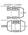
光ファイバ通信の分野では大容量化を図るために、波長多重システムが用いられている。波長多重システムでは、図10に示すように波長ごとに光源と光変調器を用意する必要があり、送信部分が複雑になるという問題がある。 In the field of optical fiber communication, a wavelength division multiplexing system is used to increase the capacity. In the wavelength multiplexing system, as shown in FIG. 10, it is necessary to prepare a light source and an optical modulator for each wavelength, and there is a problem that a transmission part becomes complicated.
この問題を解決する提案としては、例えば特許文献1に開示されているような多波長成分を一括して発生させる多波長光源がある。しかし、この多波長光源を用いる場合も、光変調器は波長多重チャネル数だけ必要である。
As a proposal for solving this problem, there is a multi-wavelength light source that collectively generates multi-wavelength components as disclosed in
また、特許文献2には、多波長一括光変調装置が開示されている。これを図11に示す。この装置では、入力された光信号を波長合分波手段により、それぞれの光搬送波の信号に分け、その光搬送波の数に応じた光強度変調器と、その個数に等しい光回帰手段を用いて光変調装置を構成している。この場合も、多数の光強度変調器を用いることになり、装置構成が複雑になるという問題があった。
また、非特許文献3には、光変調器を用いた光周波数コムの発生器が報告されているが、これは、1波長の光についてのものであり、この点において本発明とは異なっている。
Further, Non-Patent
この発明は、従来なかった形態の光変調器を提案しており、複数の周波数帯の光の変調を、単一の光変調器で行なうものである。 The present invention proposes an optical modulator of an unconventional form, in which light in a plurality of frequency bands is modulated by a single optical modulator.
この発明により、単一あるいは少数の光変調器で、複数あるいは多数の光信号を、それぞれの変調信号で変調することができる多波長一括光変調および多波長一括光変調器を実現する。 According to the present invention, a multi-wavelength collective optical modulator and a multi-wavelength collective optical modulator capable of modulating a plurality or a large number of optical signals with respective modulation signals with a single or a small number of optical modulators are realized.
まず、本発明の原理を説明する。
図1(a)は、本発明の単位構成となる光変調器の模式図である。光ファイバの光路1上には、入力側の反射手段としてFBG3(ファイバブラッグ格子)が設けられ、また、出力側の反射手段としてFBG4が設けられている。これらの反射手段の中間の位置には、光強度変調手段として光変調器2が設けられている。この光変調器2は、変調信号の波長よりも短い変調電極を持った共振型の強度変調器であるとする。また、FBG4は、図1(c)に示すような反射帯域をもち、FBG3は、図1(b)に示すように、2つの反射帯域とそれに挟まれた1つの透過帯域をもっている。FBG4の反射帯域の幅と、FBG3の2つの反射帯域に渡る幅は、等しいものとする。
First, the principle of the present invention will be described.
Fig.1 (a) is a schematic diagram of the optical modulator used as the unit structure of this invention. On the
光路1には、上記の透過帯域内の波長を持ったレーザ光を入射する。このレーザ光は、FBG3を通過後に、光強度変調手段で変調され、側帯波を伴った信号になり、FBG4で反射される。この反射により、側帯波を伴った信号は光変調器2でさらに変調され、光搬送波と、1次と2次の側帯波を伴って、FBG3に達する。ここで、光搬送波は、光路の入射部の方に進み共振器の外部に棄却される。側帯波は再び、反射され変調されることにより、1次、2次、および3次の側帯波と僅かな強度ながら光搬送波の信号成分を持った光信号がFBG4に達する。ここで、もし、3次の側帯波がFBG4の反射帯域の外に位置している場合は、この3次の側帯波のみがFBG4を通過して共振器の外部に出力される。このような反射により次回に光信号がFBG4に戻るときにも、1次、2次、および3次の側帯波と僅かな強度ながら光搬送波の信号成分を持った光信号であり、3次の側帯波成分が共振器から出力される。このように、最短で出力される光信号は、反射を3回繰り返した後に出力される場合は、3次の側帯波が出力される。
Laser light having a wavelength within the above transmission band is incident on the
ここで、図2(a)に示すように、光パルスが強度変調器で変調される場合を考える。変調信号が正弦波の場合には、その尖頭値を結ぶ線は正弦波になることが知られている。また、横軸にパルスの位置をとり、縦軸に同じ時点での変調電極の電位をとると、正弦波が得られることも知られている。これを、共振器の中を光パルスが伝搬する場合にプロットすると、図2(b)のようになることが分かる。図2(b)においては、光パルスが、変調電極の電位がピークの時に最初に光変調器を通過し、2度目、3度目に光変調器を通過する際も変調電極の電位はピークのときである。この場合は、最も強い3次の側帯波が得られる事が分かる。この様に、変調信号の周期は、光パルスが光変調器からFBG3あるいはFBG4までの往復に要する時間の自然数分の1に等しいことが望ましいことがわかる。特に、変調信号の周期が、その往復に要する時間の奇数(あるいは偶数)分の1に等しい場合には、往路と復路とでは光波がうける変調信号は逆相(あるいは同相)になるようにする事が望ましい。
Here, as shown in FIG. 2A, consider a case where an optical pulse is modulated by an intensity modulator. When the modulation signal is a sine wave, it is known that the line connecting the peak values is a sine wave. It is also known that a sine wave can be obtained by taking the position of the pulse on the horizontal axis and the potential of the modulation electrode at the same time on the vertical axis. When this is plotted when the optical pulse propagates through the resonator, it can be seen that FIG. In FIG. 2B, when the light pulse passes through the optical modulator first when the potential of the modulation electrode is at the peak and passes through the optical modulator for the second and third times, the potential of the modulation electrode is at the peak. Is the time. In this case, it can be seen that the strongest third-order sideband is obtained. In this way, it can be seen that the period of the modulation signal is preferably equal to a natural fraction of the time required for the optical pulse to travel back and forth from the optical modulator to the
また、図2(b)では、FBG3とFBG4との中間点に変調電極を配置した例を示したが、変調電極は、このように中間点にある必要はなく、FBG3側かFBG4側にずれた配置でもよい。但し、この場合は、FBG3からFBG4へ向かう光波を変調する変調信号と、その逆に進む光波を変調する変調信号には、その位置的なずれによる位相差を設ける事が望ましい。
FIG. 2B shows an example in which the modulation electrode is arranged at the intermediate point between the
このようにして側帯波を得る場合は、共振器の光路長によって、用いることのできる変調信号の周波数帯が決まってくる。これは、変調信号に種々の周波数の信号が重ね合わされている場合でも、共振器の光路長を調整することによって、変調信号の周波数を選択できることを意味している。 When sideband waves are obtained in this way, the frequency band of the modulation signal that can be used is determined by the optical path length of the resonator. This means that even when signals of various frequencies are superimposed on the modulation signal, the frequency of the modulation signal can be selected by adjusting the optical path length of the resonator.
このため、本発明は、次のようにする事により多波長一括光変調器を実現するものである。入力フィルタと単一の光変調器と出力フィルタとが同一の光路上にあって、上記入力フィルタを通して上記光変調器に、各チャネルnの光成分の周波数がfnである多波長光を一括して入力し、上記入力フィルタを通して上記光変調器に一括して入力された上記多波長光は、上記入力フィルタと上記出力フィルタとで反射されて往復し、往復するたびに、上記多波長光の各チャネルnの光成分に対応して変調周波数Fnの変調信号が印加される上記光変調器で上記多波長光の各チャネルnの光成分が変調を受けて、上記多波長光の各チャネルnの光成分に対応して周波数fn+i k Fnの側帯波(i k は整数であり、側帯波の次数である。)を発生させ、上記側帯波の周波数が上記出力フィルタあるいは上記入力フィルタで決められた反射帯域外の周波数に達した場合に上記出力フィルタあるいは上記入力フィルタを通って出力される多波長一括光変調方法または多波長一括光変調装置において、
上記多波長光の各チャネルnの光成分が上記往復に要する時間は、上記各変調信号の1周期(=1/Fn)の整数倍であるものとする。
For this reason, the present invention realizes a multi-wavelength collective optical modulator by the following manner. The input filter, the single optical modulator, and the output filter are on the same optical path, and the multi-wavelength light whose frequency of the optical component of each channel n is fn is bundled into the optical modulator through the input filter. The multi-wavelength light that is input to the optical modulator in a batch through the input filter is reflected by the input filter and the output filter, and reciprocates. The optical modulator to which the modulation signal of the modulation frequency Fn is applied corresponding to the optical component of each channel n is modulated by the optical component of each channel n of the multi-wavelength light, and each channel n of the multi-wavelength light The sideband wave of frequency fn + i k Fn (i k is an integer and the order of the sideband wave) is generated corresponding to the optical component of the light wave, and the frequency of the sideband wave is determined by the output filter or the input filter. Reflection zone In simultaneous multi-wavelength optical modulation method or multi-wavelength optical modulation device output through the output filter or the input filter when it reaches the outside of the frequency,
The time required for the light component of each channel n of the multi-wavelength light to reciprocate is an integral multiple of one period (= 1 / Fn) of each modulated signal .
また、本発明は、上記多波長光の各チャネルnの光成分の上記の往復に要する時間が、上記変調信号の1周期(=1/Fn)の奇数倍の時には、上記の光変調器は、往路と復路とで上記各チャネルnの光成分を逆相で変調し、あるいは、上記変調信号の1周期(=1/Fn)の偶数倍の時には、往路と復路とで上記各チャネルnの光成分を同相で変調するものである。In the present invention, when the time required for the round trip of the optical component of each channel n of the multi-wavelength light is an odd multiple of one period (= 1 / Fn) of the modulated signal, the optical modulator is The optical component of each channel n is modulated in the reverse phase in the forward path and the return path, or when the modulated signal is an even multiple of one period (= 1 / Fn) of each channel n in the forward path and the return path. The light component is modulated in phase.
さらに、
3)−(An−1)から(Bn−1)までの0以外の整数ikについて、和、fn+ikFn、について重なりが無い、
あるいは、
4)チャネルnの各成分が上記の往復に要する時間が、他のチャネルの変調周波数の1周期の整数倍に一致しない、
などの条件を満たすことが望ましい。しかし、前記の4)については、例えば、一致する場合でも、次の場合は動作可能である。つまり、2つのチャネルが重なる場合で、上記の往復時間が一方の奇数倍で、他方の偶数倍となるときで、しかも、
(遅延量)=(1/Fn)×P=(1/Fm)×Q
で、P、Qのどちらか一方が奇数、もう一方が偶数である場合である。さらに、僅かな混信を許してもよい場合には、3)あるいは4)の条件を必ずしも満たす必要は無い。
further,
3) There is no overlap for the sum, f n + i k F n , for integers i k other than 0 from − (A n −1) to (B n −1),
Or
4) The time required for each component of the channel n to make the round trip does not match an integral multiple of one period of the modulation frequency of the other channel.
It is desirable to satisfy the following conditions. However, with regard to 4) above, for example, even if they match, the operation is possible in the following cases. In other words, when two channels overlap, the round trip time is an odd multiple of one and an even multiple of the other, and
(Delay amount) = (1 / Fn) × P = (1 / Fm) × Q
In this case, one of P and Q is an odd number and the other is an even number. Furthermore, when a slight interference may be allowed, it is not always necessary to satisfy the condition 3) or 4).
また、本発明は、上記出力フィルタは、予め決めたられた反射帯域を有する出力フィルタであり、上記入力フィルタは、該反射帯域と共通の周波数帯域を有する反射帯域をそれぞれもつ第1と第2の反射帯域と、第1と第2の反射帯域とに挟まれた透過帯域とを備えた入力フィルタであって、該出力フィルタと該入力フィルタとを単位構成とするとき、
上記出力フィルタの反射帯域がそれぞれ異なる複数の単位構成が上記同一の光路上にあって、上記単一の光変調器を共有するものであり、
上記光変調器は、強度変調器あるいは位相変調器であって、
上記光変調器の入射光あるいは出射光は、上記の複数の単位構成で反射された光である事を特徴とする。
According to the present invention, the output filter is an output filter having a predetermined reflection band, and the input filter has first and second reflection bands each having a reflection band having a frequency band in common with the reflection band. When the input filter includes a reflection band and a transmission band sandwiched between the first and second reflection bands, and the output filter and the input filter have a unit configuration,
A plurality of unit configurations each having a different reflection band of the output filter are on the same optical path and share the single optical modulator,
The optical modulator is an intensity modulator or a phase modulator,
Incident light or outgoing light of the light modulator is light reflected by the plurality of unit configurations .
また本発明は、上記入力フィルタは、第1と第2の反射帯域をもち、前記の第1と第2の反射帯域とに挟まれた透過帯域を通して上記多波長光を入力するフィルタであり、上記出力フィルタは、櫛歯状の反射特性をもち上記変調信号と同数の櫛歯状反射特性部を備え、前記の櫛歯状反射特性部のそれぞれは、それぞれの上記変調周波数の自然数倍の、または、それぞれの上記変調周波数の自然数分の1の、自由スペクトルレンジの反射特性を持ち、入力した上記多波長光の各チャネルnの光成分を変調して得られる搬送波、一次側帯波、あるいは高次側帯波のいずれかが、上記各チャネルごとに異なった櫛歯状反射特性部で反射される事を特徴とする。 In the present invention, the input filter has a first and second reflection bands, and inputs the multi-wavelength light through a transmission band sandwiched between the first and second reflection bands. The output filter has comb-like reflection characteristics and the same number of comb-like reflection characteristics as the modulation signal, and each of the comb-like reflection characteristics has a natural number times the modulation frequency. Or a carrier wave obtained by modulating the optical component of each channel n of the input multi-wavelength light having a free spectral range reflection characteristic that is a natural fraction of each of the modulation frequencies, or a primary sideband, or Any one of the higher-order sideband waves is reflected by a comb-like reflection characteristic portion that is different for each channel.
あるいは、上記出力フィルタは、入力した上記多波長光の各チャネルnの光成分を反射することができる予め決められた反射帯域をもつフィルタであり、 Alternatively, the output filter is a filter having a predetermined reflection band capable of reflecting the light component of each channel n of the input multi-wavelength light,
上記入力フィルタは、櫛歯状の反射特性をもち上記変調信号と同数の櫛歯状反射特性部を備え、前記の櫛歯状反射特性部のそれぞれは、それぞれの上記変調周波数の2以上の自然数倍の自由スペクトルレンジの反射特性を持ち、入力した上記多波長光のそれぞれの光波を2度変調して得られる搬送波、一次側帯波、あるいは高次側帯波のひとつのいずれかが、上記各チャネルごとに異なった櫛歯状反射特性部で反射される、The input filter has comb-like reflection characteristics and has the same number of comb-like reflection characteristics as the modulation signal, and each of the comb-like reflection characteristics has two or more natural frequencies of the modulation frequency. One of the carrier wave, the primary sideband wave, and the high-order sideband wave obtained by modulating the light wave of each of the inputted multi-wavelength light twice, having a reflection characteristic of several times the free spectral range, Reflected by different comb-like reflection characteristics for each channel,
ことを特徴とする。It is characterized by that.
また、本発明は、上記光変調器に、共振型の変調電極を用いた強度変調器あるいは位相変調器を用いることを特徴とする。あるいは、上記光変調器に、進行波型の強度変調器あるいは位相変調器を用いることを特徴とする。 The present invention is also characterized in that an intensity modulator or a phase modulator using a resonance type modulation electrode is used for the optical modulator. Alternatively, a traveling wave type intensity modulator or phase modulator is used as the optical modulator.
以下に、この発明の実施の形態を図面に基づいて詳細に説明する。以下の説明においては、同じ機能あるいは類似の機能をもった装置に、特別な理由がない場合には、同じ符号を用いるものとする。 Embodiments of the present invention will be described below in detail with reference to the drawings. In the following description, devices having the same function or similar functions are denoted by the same reference numerals unless there is a special reason.
先ず本発明の実施例を図3を用いて説明する。図3(a)は、200THzと199THzの光をひとつの変調器を用いて変調する構成を示すブロック図である。光路1に沿って、入力端、入力側FBG5、入力側FBG3、光変調器2、出力側FBG4、出力側FBG6、出力端が配置されている。ここで、FBG5、FBG3、の反射特性は、図3(b)に示すように、それぞれ1GHzの透過帯域を挟んで、それぞれ13.5GHzの2つの反射帯域と、それぞれ22.5GHzの2つの反射帯域とで構成されている。また、FBG6、FBG4の反射特性は、FBG5、FBG3の特性から透過帯域が消えた場合に相当する反射特性を持っている。これらの反射特性の上限と下限とは、一致する必要がなく、変調周波数のほぼ半分程度の誤差で作られていればよい。また、上記の透過帯域は、光を完全に透過する必要はなく、僅かに反射する特性であってもよい。
First, an embodiment of the present invention will be described with reference to FIG. FIG. 3A is a block diagram showing a configuration for modulating light of 200 THz and 199 THz using a single modulator. An input end, an
これらのFBG、光変調器、光路などを光信号が伝搬するために要する時間は、入力端からの遅延時間で表すものとして、FBG3、4、5、6は共に、100p秒(透過時間)/50p秒(反射時間)の遅延時間を示し、FBG3−FBG4間は、光変調器を含めて150p秒の遅延時間を示し、FBG5とFBG3間あるいはFBG4とFBG6間は50p秒の光伝搬遅延時間の長さで作られているものとする。このとき、FBG3とFBG4で形成される光共振器1を光信号が往復するために要する時間は、400p秒であり、FBG5とFBG6で形成される光共振器2を光信号が往復するために要する時間は、1000p秒である。
The time required for an optical signal to propagate through these FBGs, optical modulators, optical paths, etc. is expressed as a delay time from the input end, and
光共振器1では、往復で変調されるとすると、上記の遅延時間(400p秒)から、5GHzの変調信号(200p秒の周期)を印加することになる。また、光共振器2でも往復で変調されるとすると、1GHz(1000p秒の周期)の変調信号を印加することができるが、その高調波に相当する周波数の変調信号によっても往復で変調できる事は明らかである。このため、その高調波に相当する周波数の変調信号を同時に光変調器2に印加する。このように同時に印加する例として、光共振器1には、5GHzの変調信号を選択し、光共振器2には、4GHz(250p秒の周期)の変調信号を選択する。このため、出力フィルタからの制限を受けて、光共振器1からは、出力端に5次の側帯波が出力され、光共振器2からは、出力端に4次と5次の側帯波が出力される。
If the
5GHzの変調信号あるいは4GHzの変調信号としては、5GHzの搬送波あるいは4GHzの搬送波を変調して得た5GHzあるいは4GHzの回りに分布する信号を、光信号の変調信号として用いても、上記の議論は、無視しうる誤差で成立することは、容易に理解できる。 Even if a signal distributed around 5 GHz or 4 GHz obtained by modulating a 5 GHz carrier wave or a 4 GHz carrier wave is used as a 5 GHz modulation signal or a 4 GHz modulation signal, the above argument can be used. It can be easily understood that the error can be ignored.
図3に示した多波長一括光変調器については、入力するレーザ光の波長と、光共振器の光路長との整合性をとる必要がある。また、光共振器の光路長は、変調信号の周波数との整合もとる必要がある。これは、例えば、非特許文献2で公表されているような熱膨張で光路長を調整させる素子(光路長調整素子)を用いて整合をとることができる。このような光路長調整素子は、種々のものが知られているが、本発明の多波長一括光変調器の光路に収まるサイズのものであることが肝要である。また、図5に示すように、それぞれの光共振器の光路長を調整できるように、それぞれの共振器に設けることが望ましい。
In the multi-wavelength batch optical modulator shown in FIG. 3, it is necessary to match the wavelength of the input laser beam and the optical path length of the optical resonator. Further, the optical path length of the optical resonator needs to be matched with the frequency of the modulation signal. This can be matched, for example, using an element (optical path length adjusting element) that adjusts the optical path length by thermal expansion as disclosed in
上記の多波長一括光変調器の例では、2つの光共振器が1つの光変調器を共有しているが、さらに多数の光共振器が1つの光変調器を共有する構成にすることにより、さらに多数の波長の光信号を一括して変調できることは、明らかである。 In the example of the multi-wavelength optical modulator described above, two optical resonators share one optical modulator, but a configuration in which a larger number of optical resonators share one optical modulator is adopted. It is obvious that optical signals having a larger number of wavelengths can be modulated at once.
上記の例では、利用する波長区間に渡って一様な反射特性をもった入力フィルタ、出力フィルタの場合を示したが、櫛形の反射特性を示すものを用いても、同様の機能を実現でき、次にこれを示す。 In the above example, an input filter and an output filter having uniform reflection characteristics over the wavelength range to be used have been shown, but the same function can be realized even if a filter having a comb-like reflection characteristic is used. This is shown next.
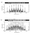
図4は、超格子型のファイバ格子の反射特性を示す図である。図4(a)は、0.4mm長の1種類のFGBを2mmピッチで並べた場合の反射特性を示し、図4(b)は、それぞれ0.4mm長の2種類のFBGを2mmピッチで並べた場合の反射特性を示している。これらの図からわかるように、櫛歯状の反射スペクトル特性の設計における自由度は高い。 FIG. 4 is a diagram showing the reflection characteristics of a superlattice type fiber grating. FIG. 4A shows the reflection characteristics when one type of 0.4 mm long FGB is arranged at a pitch of 2 mm, and FIG. 4B shows two types of 0.4 mm long FBGs at a pitch of 2 mm. The reflection characteristics when arranged are shown. As can be seen from these figures, the degree of freedom in designing the comb-like reflection spectral characteristics is high.
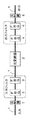
図5は、このような超格子型のファイバ格子を2つ出力フィルタに用いた本発明の実施例を示す。図5(a)に示すように、この多波長一括変調器は、FBGaによる入力フィルタと、FBGcとFBGdとのよる出力フィルタと、これらのフィルタ間に設けられた光変調器からなっている。この多波長一括変調器には、2つの光波が入力され、2系統の変調信号が供給される。この2つの光波は、入力フィルタを透過するが、その光波が変調されることによって発生する側帯波を反射する特性を持っている。図5の例では、光波と変調信号の数をそれぞれ2にしたが、その数がこれより大きい場合でも、容易に多波長一括変調器を実現することができる。 FIG. 5 shows an embodiment of the present invention in which two such superlattice fiber gratings are used as output filters. As shown in FIG. 5A, the multi-wavelength modulator includes an FBGa input filter, an FBGc and FBGd output filter, and an optical modulator provided between these filters. Two light waves are input to this multi-wavelength batch modulator, and two types of modulation signals are supplied. These two light waves pass through the input filter, but have a characteristic of reflecting sideband waves generated when the light waves are modulated. In the example of FIG. 5, the number of light waves and modulation signals is two, but even when the number is larger than this, a multi-wavelength batch modulator can be easily realized.
FBGaの反射特性は、図5(b)に示すように、入力した光波を透過するが、その光波を変調して得られた側帯波を反射する特性を持つものである。また、例えば、入力する光波は200THz(λa)と200.0005THz(λb)、入力フィルタの透過帯域幅は2GHz、その反射帯域幅は200THz±2GHzから200THz±18GHzである。また、λa、λbの光波をそれぞれ、8GHz、5GHzで変調するものとする。また、FBGc、FBGdのFSRは、それぞれ16GHz、10GHzである。 As shown in FIG. 5B, the reflection characteristics of FBGa have a characteristic of transmitting an input light wave but reflecting a sideband wave obtained by modulating the light wave. Also, for example, the input light waves are 200 THz (λa) and 200.0005 THz (λb), the transmission filter has a transmission bandwidth of 2 GHz, and its reflection bandwidth is 200 THz ± 2 GHz to 200 THz ± 18 GHz. Further, it is assumed that the light waves of λa and λb are modulated at 8 GHz and 5 GHz, respectively. The FSRs of FBGc and FBGd are 16 GHz and 10 GHz, respectively.
ここで、FBGcの反射スペクトルのフリンジは、λaの光波を8GHzの変調信号で多重変調することにより発生する側波帯の位置に合致するようにする。同様に、FBGdの反射スペクトルのフリンジは、λbの光波を5GHzの変調信号で多重変調することにより発生する側波帯の位置に合致するように設定する。λaの光波を5GHzの変調信号で変調した側帯波、あるいは、λbの光波を8GHzの変調信号で変調した側帯波は、一度だけ変調を受けるだけで出力側に送られる。 Here, the fringe of the reflection spectrum of the FBGc is made to coincide with the position of the sideband generated by multiplexing the light wave of λa with the modulation signal of 8 GHz. Similarly, the fringe of the reflection spectrum of FBGd is set so as to match the position of the sideband generated by multiplex-modulating the light wave of λb with the modulation signal of 5 GHz. A sideband wave obtained by modulating a light wave of λa with a modulation signal of 5 GHz or a sideband wave obtained by modulating a light wave of λb with a modulation signal of 8 GHz is sent to the output side only after being modulated once.
変調信号に情報が重畳されているときには、側波帯の幅は広がるので、フリンジの幅は、そのような側波帯をカバーできるような幅を設定する必要がある。しかし、ここでは、説明を簡単にするために、変調信号は単純な正弦波であるとし、個々のフリンジの幅は200MHzであるとする。する。また、有効なフリンジの数は、それぞれFBGc、FBGdの構造で決めることができる。FBGc、FBGdのサイズを大きくとることができる場合は、図5に示したように、反射に有効なフリンジの数を少なくすることができ、その外側に位置する側帯波を出力することができる。しかし、そのサイズを大きく取れないときには、フリンジは、広い波長帯域に広がるので、出力される光波は、フリンジ間をすり抜けることのできる光波である。図5(b)、(c)の配置では、奇数次の側帯波をブロックするようにFBGc、FBGdを配置している。 When information is superimposed on the modulation signal, the width of the sideband is widened, so the width of the fringe needs to be set so as to cover such a sideband. However, here, in order to simplify the explanation, it is assumed that the modulation signal is a simple sine wave, and the width of each fringe is 200 MHz. To do. The number of effective fringes can be determined by the structures of FBGc and FBGd, respectively. When the sizes of FBGc and FBGd can be increased, as shown in FIG. 5, the number of fringes effective for reflection can be reduced, and sidebands located outside thereof can be output. However, when the size cannot be increased, the fringe spreads over a wide wavelength band, so that the output light wave is a light wave that can pass through the fringe. 5B and 5C, FBGc and FBGd are arranged so as to block odd-order sidebands.
ここで、偶数時の側帯波をブロックして奇数次の側帯波を出力するためには、図6(c)に示すように、λbの光波をブロックする周波数位置にフリンジを配置する。このような、構成によって、λa、λbそれぞれの光波を、それぞれの変調信号で変調し、しかも、λaについては偶数次の側帯波、λbについては奇数次の側帯波を得ることができる。フリンジの位置を変えることによって、この逆の組み合わせをもった出力を得る事は容易である。また、0次の光波をブロックするように、双方のフリンジを調整することによって、どちらも偶数次の側帯波を得ることができる。 Here, in order to block the even sideband and output the odd-order sideband, as shown in FIG. 6C, a fringe is arranged at a frequency position where the light wave of λb is blocked. With such a configuration, it is possible to modulate the light waves of λa and λb with the respective modulation signals, and to obtain even-order sideband waves for λa and odd-order sideband waves for λb. By changing the position of the fringe, it is easy to obtain an output with the reverse combination. Further, by adjusting both fringes so as to block the zeroth-order light wave, both can obtain even-order sideband waves.
以上のような多波長一括光変調器では、λaの光波を8GHzの変調信号で変調した側帯波、あるいは、λbの光波を5GHzの変調信号で変調した側帯波などの、種々の光波が混在しているので、実用に供する場合には、図7のブロック図のAの位置に示すフィルタをもうけて、このような光波のなかから特定の周波数の光波を選択して出力することが望ましい。この際、新たに設けたフィルタにより反射波が発生する場合は、この反射波との干渉を避けるために、入力フィルタと新たに設けたフィルタとを往復する光波が、いずれの変調信号の周期よりも大きな遅延時間を持つように設定することが望ましい。 In the multi-wavelength optical modulator as described above, various light waves such as a sideband wave obtained by modulating a light wave of λa with a modulation signal of 8 GHz or a sideband wave obtained by modulating a light wave of λb with a modulation signal of 5 GHz are mixed. Therefore, for practical use, it is desirable to provide a filter shown at the position A in the block diagram of FIG. 7 and select and output a light wave having a specific frequency from such a light wave. At this time, when a reflected wave is generated by the newly provided filter, in order to avoid interference with the reflected wave, the light wave that reciprocates between the input filter and the newly provided filter is transmitted from any modulation signal cycle. It is desirable to set so as to have a large delay time.
上記の図5あるいは6に示す構成において、λa、λbの光波をそれぞれ、8GHz、5GHzで変調するためには、上述したように、変調信号のあるいはその高調波の周期と光信号が多重往復する際の1往復に要する時間とを整合させる必要がある。この様な整合条件は、例えば、入力フィルタあるいは出力フィルタが図5(a)に示す遅延時間を、持つ場合に満足することが出来る。FBGa、FBGc、FBGdの、透過遅延時間と反射遅延時間は、それぞれ、100p秒と50p秒である。FBGcのFBGa側とFBGd側のそれぞれの光路には50p秒の伝搬遅延光路が設けられているものとする。FBGa−FBGcの接続端間の遅延時間は、150p秒である。このとき、FBGaとFBGc間を多重往復する光路の1往復の遅延時間は、500p秒である。また、FBGaとFBGd間を多重往復する光路の1往復の遅延時間は、800p秒である。これらの値(つまり500p秒、800p秒)は、8GHz(周期125p秒)、5GHz(周期200p秒)の信号のそれぞれ4倍の周期である。 In the configuration shown in FIG. 5 or 6 described above, in order to modulate the light waves of λa and λb at 8 GHz and 5 GHz, respectively, as described above, the period of the modulation signal or its harmonics and the optical signal are multiplexed and reciprocated. It is necessary to match the time required for one round trip. Such a matching condition can be satisfied, for example, when the input filter or the output filter has the delay time shown in FIG. The transmission delay time and the reflection delay time of FBGa, FBGc, and FBGd are 100 psec and 50 psec, respectively. It is assumed that a propagation delay optical path of 50 psec is provided in each of the optical paths on the FBGa side and the FBGd side of FBGc. The delay time between the connection ends of FBGa-FBGc is 150 ps. At this time, the delay time of one round trip of the optical path that makes multiple round trips between FBGa and FBGc is 500 ps. In addition, the delay time for one round trip of the optical path that makes multiple round trips between FBGa and FBGd is 800 psec. These values (that is, 500 psec and 800 psec) are four times as long as signals of 8 GHz (cycle 125 psec ) and 5 GHz (cycle 200 psec ), respectively .
図5あるいは図6のFBGcとFBGdとのフリンジが重なるような場合は、λaの光波を5GHzの変調信号で変調した側帯波、あるいは、λbの光波を8GHzの変調信号で変調した側帯波などが混在した出力を得ることになり混信の原因になるが、これは重なりの頻度に依存している。実用においてこのような混信が許容される環境であれば、このような設定も許されることは明らかである。 When the fringes of FBGc and FBGd in FIG. 5 or FIG. 6 overlap, a sideband wave obtained by modulating a light wave of λa with a 5 GHz modulation signal, a sideband wave obtained by modulating a light wave of λb with a modulation signal of 8 GHz, or the like. This results in mixed output and causes interference, but this depends on the frequency of overlap. Obviously, such a setting is allowed in an environment where such interference is allowed in practice.
上記の例では、超格子型のファイバ格子を2つ出力フィルタに用いた実施例を示したが、図8に、超格子型のファイバ格子を2つ入力フィルタ(FBGa、FBGb)に用いた実施例を示す。この場合は、FBGdとしては、1つの連続した反射特性を持ったFBGを用いることができる。また、FBGa、FBGbの反射特性を示すフリンジとしては、実施例2にけるFBGc、FBGdと同様な条件を満たすものを用いることができる。 In the above example, an example in which two superlattice type fiber gratings are used for the output filter is shown. However, FIG. 8 shows an example in which two superlattice type fiber gratings are used for the input filter (FBGa, FBGb). An example is shown. In this case, as the FBGd, an FBG having one continuous reflection characteristic can be used. Further, as the fringe showing the reflection characteristics of FBGa and FBGb, those that satisfy the same conditions as FBGc and FBGd in Example 2 can be used.
しかし、この実施例の場合においても、λaの光波を8GHzの変調信号で変調した側帯波、あるいは、λbの光波を5GHzの変調信号で変調した側帯波などの、種々の光波が混在しているので、実用に供する場合には、図7のブロック図のBの位置に示すフィルタをもうけて、このような光波のなかから特定の周波数の光波を選択して出力することが望ましい。この際も上記の場合と同様に、新たに設けたフィルタにより反射波が発生する場合は、この反射波との干渉を避けるために、入力フィルタと新たに設けたフィルタとを往復する光波が、いずれの変調信号の周期よりも大きな遅延時間を持つように設定することが望ましい。 However, even in this embodiment, various light waves such as a sideband wave obtained by modulating a light wave of λa with a modulated signal of 8 GHz or a sideband wave obtained by modulating a light wave of λb with a modulated signal of 5 GHz are mixed. Therefore, in practical use, it is desirable to provide a filter shown at position B in the block diagram of FIG. 7 and select and output a light wave having a specific frequency from such a light wave. At this time, similarly to the above case, when a reflected wave is generated by a newly provided filter, in order to avoid interference with this reflected wave, a light wave that reciprocates between the input filter and the newly provided filter is It is desirable to set so as to have a delay time longer than the period of any modulation signal.
図9は、図2の多波長一括光変調器を用いて構成した光周波数コムの発生器を示す。これは、図2の多波長一括光変調器を光共振器のなかに設けたものである。この光共振器は、用いる光スペクトルについて、良好な反射特性と、僅かな透過特性を備えるものであり、ファブリペロー型光共振器や、FGBを反射器に用いた光ファイバ上の光共振器でもよいことは明らかである。 FIG. 9 shows an optical frequency comb generator configured using the multi-wavelength batch optical modulator of FIG. In this configuration, the multi-wavelength collective optical modulator of FIG. 2 is provided in an optical resonator. This optical resonator has good reflection characteristics and slight transmission characteristics with respect to the optical spectrum to be used. Even an Fabry-Perot type optical resonator or an optical resonator on an optical fiber using FGB as a reflector is used. It is clear that it is good.
上記の光周波数コム発生器は、変調周波数の整数倍の周波数で変調する場合と透過な変調特性が得られる点と、異なる波長の光による光周波数コムを同時に発生することができる点は、従来にない特徴である。 The above-mentioned optical frequency comb generator is capable of generating a transparent modulation characteristic when modulated at a frequency that is an integral multiple of the modulation frequency, and is capable of simultaneously generating optical frequency combs using light of different wavelengths. It is a feature that is not present.
本発明の多波長一括光変調器を、所謂ファイバ無線システムとして知られる、光ファイバを用いてミリ波信号を送信する装置に適用することにより、光信号の変調に必要な変調器の数を減少させることができる。また、本発明の多波長一括光変調器を用いて光周波数コム発生器を構成することにより、異なる波長の光による光周波数コムを同時に発生することができる。 By applying the multi-wavelength optical modulator of the present invention to an apparatus that transmits a millimeter wave signal using an optical fiber, which is known as a so-called fiber radio system, the number of modulators required for modulating the optical signal is reduced. Can be made. Further, by configuring the optical frequency comb generator using the multi-wavelength collective optical modulator of the present invention, it is possible to simultaneously generate optical frequency combs using light of different wavelengths.
1 光路
2 光変調器
3 入力側FBG
4 出力側FBG
5 入力側FBG
6 出力側FBG
7 反射鏡
8 反射鏡
10 入力フィルタ
11 出力フィルタ
13、14 フィルタ
15 分岐器
1
4 Output side FBG
5 Input side FBG
6 Output side FBG
7 reflecting mirror 8 reflecting
Claims (9)
上記入力フィルタを通して上記光変調器に、各チャネルnの光成分の周波数がfnである多波長光を一括して入力し、
上記入力フィルタを通して上記光変調器に一括して入力された上記多波長光は、上記入力フィルタと上記出力フィルタとで反射されて往復し、往復するたびに、上記多波長光の各チャネルnの光成分に対応して変調周波数Fnの変調信号が印加される上記光変調器で上記多波長光の各チャネルnの光成分が変調を受けて、上記多波長光の各チャネルnの光成分に対応して周波数fn+i k Fnの側帯波(i k は整数であり、側帯波の次数である。)を発生させ、上記側帯波の周波数が上記出力フィルタあるいは上記入力フィルタで決められた反射帯域外の周波数に達した場合に上記出力フィルタあるいは上記入力フィルタを通って出力される多波長一括光変調方法において、
上記多波長光の各チャネルnの光成分が上記往復に要する時間は、上記各変調信号の1周期(=1/Fn)の整数倍であることを特徴とする多波長一括光変調方法。 The input filter, the single optical modulator and the output filter are on the same optical path,
The multi-wavelength light whose frequency of the light component of each channel n is fn is collectively input to the optical modulator through the input filter ,
The input the multi-wavelength light inputted collectively to the optical modulator through the filter reciprocates is reflected by the said input filter and the output filter, each time the round trip, for each channel n of the multi-wavelength light In the optical modulator to which a modulation signal having a modulation frequency Fn is applied corresponding to the optical component, the optical component of each channel n of the multi-wavelength light is modulated and converted into the optical component of each channel n of the multi-wavelength light. sideband frequency fn + i k Fn corresponding (i k is an integer, the order of the sideband.) to generate, out of the reflection band frequency is determined by the output filter or the input filter of the sidebands in simultaneous multi-wavelength optical modulation method is output through the output filter or the input filter when reaching the frequency,
The multi-wavelength optical modulation method characterized in that the time required for the optical component of each channel n of the multi-wavelength light to reciprocate is an integral multiple of one period (= 1 / Fn) of each modulation signal.
上記入力フィルタを通して上記光変調器に、各チャネルnの光成分の周波数がfnである多波長光を一括して入力し、
上記入力フィルタを通して上記光変調器に一括して入力された上記多波長光は、上記入力フィルタと上記出力フィルタとで反射されて往復し、往復するたびに、上記多波長光の各チャネルnの光成分に対応して変調周波数Fnの変調信号が印加される上記光変調器で上記多波長光の各チャネルnの光成分が変調を受けて、上記多波長光の各チャネルnの光成分に対応して周波数fn+i k Fnの側帯波(i k は整数であり、側帯波の次数である。)を発生させ、上記側帯波の周波数が上記出力フィルタあるいは上記入力フィルタで決められた反射帯域外の周波数に達した場合に上記出力フィルタあるいは上記入力フィルタを通って出力される多波長一括光変調装置において、
上記多波長光の各チャネルnの光成分が上記往復に要する時間は、上記各変調信号の1周期(=1/Fn)の整数倍であることを特徴とする多波長一括光変調器。 The input filter, the single optical modulator and the output filter are on the same optical path,
The multi-wavelength light whose frequency of the light component of each channel n is fn is collectively input to the optical modulator through the input filter ,
The input the multi-wavelength light inputted collectively to the optical modulator through the filter reciprocates is reflected by the said input filter and the output filter, each time the round trip, for each channel n of the multi-wavelength light In the optical modulator to which a modulation signal having a modulation frequency Fn is applied corresponding to the optical component, the optical component of each channel n of the multi-wavelength light is modulated and converted into the optical component of each channel n of the multi-wavelength light sideband frequency fn + i k Fn corresponding (i k is an integer, the order of the sideband.) to generate, out of the reflection band frequency is determined by the output filter or the input filter of the sidebands in simultaneous multi-wavelength optical modulation device output through the output filter or the input filter when reaching the frequency,
The multi -wavelength collective optical modulator characterized in that the time required for the optical component of each channel n of the multi-wavelength light to reciprocate is an integral multiple of one period (= 1 / Fn) of each modulated signal.
上記出力フィルタの反射帯域がそれぞれ異なる複数の単位構成が上記同一の光路上にあって、上記単一の光変調器を共有するものであり、
上記光変調器は、強度変調器あるいは位相変調器であって、
上記光変調器の入射光あるいは出射光は、上記の複数の単位構成で反射された光である事を特徴とする請求項3に記載の多波長一括光変調器。 The output filter is an output filter having a predetermined reflection band , and the input filter has first and second reflection bands each having a reflection band having a frequency band common to the reflection band, An input filter having a transmission band sandwiched between the first and second reflection bands , wherein the output filter and the input filter have a unit configuration,
A plurality of unit configurations each having a different reflection band of the output filter are on the same optical path and share the single optical modulator,
The optical modulator is an intensity modulator or a phase modulator ,
The multi-wavelength collective light modulator according to claim 3 , wherein incident light or outgoing light of the optical modulator is light reflected by the plurality of unit configurations .
上記出力フィルタは、櫛歯状の反射特性をもち上記変調信号と同数の櫛歯状反射特性部を備え、
前記の櫛歯状反射特性部のそれぞれは、それぞれの上記変調周波数の自然数倍の、または、それぞれの上記変調周波数の自然数分の1の、自由スペクトルレンジの反射特性を持ち、
入力した上記多波長光の各チャネルnの光成分を変調して得られる搬送波、一次側帯波、あるいは高次側帯波のいずれかが、上記各チャネルごとに異なった櫛歯状反射特性部で反射される事を特徴とする請求項3に記載の多波長一括光変調器。 The input filter is a filter having first and second reflection bands and inputting the multi-wavelength light through a transmission band sandwiched between the first and second reflection bands.
The output filter includes the modulated signal the same number of comb-shaped reflection characteristic portion has a comb-shaped reflection characteristics,
Each of the comb-shaped reflection characteristic portion has a natural number multiple of each of the above modulation frequency, or natural fraction of each of the modulation frequency, the reflection characteristic of the free spectral range,
Either the carrier wave, the primary sideband wave, or the high-order sideband wave obtained by modulating the optical component of each channel n of the input multi-wavelength light is reflected by a different comb-like reflection characteristic section for each channel. The multi-wavelength collective optical modulator according to claim 3 , wherein
上記入力フィルタは、櫛歯状の反射特性をもち上記変調信号と同数の櫛歯状反射特性部を備え、
前記の櫛歯状反射特性部のそれぞれは、それぞれの上記変調周波数の2以上の自然数倍の自由スペクトルレンジの反射特性を持ち、
入力した上記多波長光のそれぞれの光波を2度変調して得られる搬送波、一次側帯波、あるいは高次側帯波のひとつのいずれかが、上記各チャネルごとに異なった櫛歯状反射特性部で反射される、
ことを特徴とする請求項3に記載の多波長一括光変調器。 The output filter is a filter having a predetermined reflection band capable of reflecting the light component of each channel n of the input multi-wavelength light ,
The input filter includes the modulated signal the same number of comb-shaped reflection characteristic portion has a comb-shaped reflection characteristics,
Each of the comb-shaped reflection characteristic portion has a reflection characteristic of the two or more natural number multiple of the free spectral range of each of the above modulation frequency,
One of the carrier wave, the primary sideband wave, and the high-order sideband wave obtained by modulating each light wave of the input multi-wavelength light twice is a comb-like reflection characteristic portion that is different for each channel. Reflected,
The multi-wavelength collective optical modulator according to claim 3 .
Priority Applications (2)
| Application Number | Priority Date | Filing Date | Title |
|---|---|---|---|
| JP2004117067A JP4635168B2 (en) | 2004-04-12 | 2004-04-12 | Multi-wavelength batch optical modulation method and multi-wavelength batch optical modulator |
| US11/103,494 US7522844B2 (en) | 2004-04-12 | 2005-04-12 | Multiple-wavelength optical modulation apparatus |
Applications Claiming Priority (1)
| Application Number | Priority Date | Filing Date | Title |
|---|---|---|---|
| JP2004117067A JP4635168B2 (en) | 2004-04-12 | 2004-04-12 | Multi-wavelength batch optical modulation method and multi-wavelength batch optical modulator |
Publications (2)
| Publication Number | Publication Date |
|---|---|
| JP2005300921A JP2005300921A (en) | 2005-10-27 |
| JP4635168B2 true JP4635168B2 (en) | 2011-02-16 |
Family
ID=35136541
Family Applications (1)
| Application Number | Title | Priority Date | Filing Date |
|---|---|---|---|
| JP2004117067A Expired - Fee Related JP4635168B2 (en) | 2004-04-12 | 2004-04-12 | Multi-wavelength batch optical modulation method and multi-wavelength batch optical modulator |
Country Status (2)
| Country | Link |
|---|---|
| US (1) | US7522844B2 (en) |
| JP (1) | JP4635168B2 (en) |
Families Citing this family (2)
| Publication number | Priority date | Publication date | Assignee | Title |
|---|---|---|---|---|
| JP5760581B2 (en) | 2011-03-25 | 2015-08-12 | 富士通株式会社 | Multi-wavelength light source |
| KR20130093839A (en) * | 2012-01-26 | 2013-08-23 | 삼성전자주식회사 | Optical transmitters and optical communication systems using thermal coupled resonance modulator |
Family Cites Families (9)
| Publication number | Priority date | Publication date | Assignee | Title |
|---|---|---|---|---|
| US3408498A (en) * | 1965-12-28 | 1968-10-29 | Bell Telephone Labor Inc | Optical modulator |
| US4208091A (en) * | 1977-03-30 | 1980-06-17 | United Technologies Corporation | Broadband microwave waveguide modulator for infrared lasers |
| JP3343241B2 (en) * | 2000-06-22 | 2002-11-11 | 独立行政法人通信総合研究所 | Multiplier light modulator |
| JP3404528B2 (en) * | 2000-06-23 | 2003-05-12 | 独立行政法人通信総合研究所 | Optical frequency converter using multiplication modulation |
| JP2002023209A (en) | 2000-07-04 | 2002-01-23 | Nec Corp | Multiwavelength light source and method for obtaining multiwavelength light beam |
| JP3516032B2 (en) * | 2001-03-19 | 2004-04-05 | 独立行政法人通信総合研究所 | Optical frequency converter |
| JP2002318374A (en) * | 2001-04-20 | 2002-10-31 | Nippon Telegr & Teleph Corp <Ntt> | Multi-wavelength batch optical modulator |
| US6643429B2 (en) * | 2001-06-07 | 2003-11-04 | Nortel Networks Limited | Dispersion compensation apparatus and method utilising sampled Bragg gratings |
| JP3732804B2 (en) * | 2001-06-13 | 2006-01-11 | 日本電信電話株式会社 | Multi-wavelength optical modulation circuit and wavelength-multiplexed optical signal transmitter |
-
2004
- 2004-04-12 JP JP2004117067A patent/JP4635168B2/en not_active Expired - Fee Related
-
2005
- 2005-04-12 US US11/103,494 patent/US7522844B2/en not_active Expired - Fee Related
Also Published As
| Publication number | Publication date |
|---|---|
| US20050238366A1 (en) | 2005-10-27 |
| JP2005300921A (en) | 2005-10-27 |
| US7522844B2 (en) | 2009-04-21 |
Similar Documents
| Publication | Publication Date | Title |
|---|---|---|
| JP3516032B2 (en) | Optical frequency converter | |
| JPH04261232A (en) | Light waveguide communication system | |
| US10261260B2 (en) | Tunable microring resonator | |
| JP2005026685A (en) | Tunable laser device and manufacturing method thereof | |
| JPH01500375A (en) | Optical signal processing method and optical element | |
| CN105655869B (en) | Multi-channel tunable laser | |
| Cheng et al. | Fully tailorable integrated-optic resonators based on chirped waveguide Moiré gratings | |
| EP1168042B1 (en) | Optical frequency converter using reciprocating modulation | |
| JP4635168B2 (en) | Multi-wavelength batch optical modulation method and multi-wavelength batch optical modulator | |
| US20030142387A1 (en) | Fast optical wavelength shifter | |
| EP1168040B1 (en) | Optical modulation system using "reciprocal" modulation | |
| JP4044503B2 (en) | Pulse light source for communication | |
| JP2017527130A (en) | Tunable laser and method for adjusting laser oscillation mode | |
| KR100237379B1 (en) | Tunable optical drop/pass filter system for wdm | |
| US7215856B2 (en) | Reconfigurable optical device for wavelength division multiplexing networks | |
| JPH08122833A (en) | Wavelength converter | |
| US7660030B2 (en) | Reciprocating optical modulation system | |
| JP3923771B2 (en) | Multi-wavelength light source | |
| JP4644180B2 (en) | Optical variable delay unit and optical variable delay device | |
| JP2021021747A (en) | Optical filter | |
| Capmany | Microwave photonic filters | |
| JPH11337894A (en) | Optical subcarrier frequency modulator | |
| Zucker et al. | All Optical Wavelength Shifter Using Laser Induced High Order Moving Grating | |
| JPH02125600A (en) | Optical exchange circuit | |
| JP2002335039A (en) | Tunable mode-locked laser |
Legal Events
| Date | Code | Title | Description |
|---|---|---|---|
| A621 | Written request for application examination |
Free format text: JAPANESE INTERMEDIATE CODE: A621 Effective date: 20070316 |
|
| A977 | Report on retrieval |
Free format text: JAPANESE INTERMEDIATE CODE: A971007 Effective date: 20100312 |
|
| A131 | Notification of reasons for refusal |
Free format text: JAPANESE INTERMEDIATE CODE: A131 Effective date: 20100420 |
|
| A521 | Request for written amendment filed |
Free format text: JAPANESE INTERMEDIATE CODE: A523 Effective date: 20100621 |
|
| A131 | Notification of reasons for refusal |
Free format text: JAPANESE INTERMEDIATE CODE: A131 Effective date: 20100803 |
|
| A521 | Request for written amendment filed |
Free format text: JAPANESE INTERMEDIATE CODE: A523 Effective date: 20101004 |
|
| TRDD | Decision of grant or rejection written | ||
| A01 | Written decision to grant a patent or to grant a registration (utility model) |
Free format text: JAPANESE INTERMEDIATE CODE: A01 Effective date: 20101019 |
|
| A01 | Written decision to grant a patent or to grant a registration (utility model) |
Free format text: JAPANESE INTERMEDIATE CODE: A01 |
|
| A61 | First payment of annual fees (during grant procedure) |
Free format text: JAPANESE INTERMEDIATE CODE: A61 Effective date: 20101026 |
|
| FPAY | Renewal fee payment (event date is renewal date of database) |
Free format text: PAYMENT UNTIL: 20131203 Year of fee payment: 3 |
|
| R150 | Certificate of patent or registration of utility model |
Free format text: JAPANESE INTERMEDIATE CODE: R150 |
|
| R250 | Receipt of annual fees |
Free format text: JAPANESE INTERMEDIATE CODE: R250 |
|
| S533 | Written request for registration of change of name |
Free format text: JAPANESE INTERMEDIATE CODE: R313533 |
|
| R350 | Written notification of registration of transfer |
Free format text: JAPANESE INTERMEDIATE CODE: R350 |
|
| R250 | Receipt of annual fees |
Free format text: JAPANESE INTERMEDIATE CODE: R250 |
|
| R250 | Receipt of annual fees |
Free format text: JAPANESE INTERMEDIATE CODE: R250 |
|
| LAPS | Cancellation because of no payment of annual fees |