EP1164740A2 - Arrangement for multicarrier modulation and multiplexing - Google Patents
Arrangement for multicarrier modulation and multiplexing Download PDFInfo
- Publication number
- EP1164740A2 EP1164740A2 EP01250209A EP01250209A EP1164740A2 EP 1164740 A2 EP1164740 A2 EP 1164740A2 EP 01250209 A EP01250209 A EP 01250209A EP 01250209 A EP01250209 A EP 01250209A EP 1164740 A2 EP1164740 A2 EP 1164740A2
- Authority
- EP
- European Patent Office
- Prior art keywords
- signal
- frequency division
- orthogonal frequency
- division multiplex
- modem circuit
- Prior art date
- Legal status (The legal status is an assumption and is not a legal conclusion. Google has not performed a legal analysis and makes no representation as to the accuracy of the status listed.)
- Granted
Links
- 238000004891 communication Methods 0.000 claims abstract description 36
- 238000000034 method Methods 0.000 claims abstract description 6
- 230000005540 biological transmission Effects 0.000 claims description 15
- 230000010363 phase shift Effects 0.000 claims description 5
- 238000010586 diagram Methods 0.000 description 12
- 101100458289 Drosophila melanogaster msps gene Proteins 0.000 description 5
- 238000010295 mobile communication Methods 0.000 description 3
- 230000009466 transformation Effects 0.000 description 3
- 238000005562 fading Methods 0.000 description 2
- 230000001413 cellular effect Effects 0.000 description 1
- 230000001629 suppression Effects 0.000 description 1
Images




Classifications
-
- H—ELECTRICITY
- H04—ELECTRIC COMMUNICATION TECHNIQUE
- H04J—MULTIPLEX COMMUNICATION
- H04J11/00—Orthogonal multiplex systems, e.g. using WALSH codes
-
- H—ELECTRICITY
- H04—ELECTRIC COMMUNICATION TECHNIQUE
- H04L—TRANSMISSION OF DIGITAL INFORMATION, e.g. TELEGRAPHIC COMMUNICATION
- H04L5/00—Arrangements affording multiple use of the transmission path
- H04L5/003—Arrangements for allocating sub-channels of the transmission path
- H04L5/0044—Allocation of payload; Allocation of data channels, e.g. PDSCH or PUSCH
- H04L5/0046—Determination of the number of bits transmitted on different sub-channels
-
- H—ELECTRICITY
- H04—ELECTRIC COMMUNICATION TECHNIQUE
- H04L—TRANSMISSION OF DIGITAL INFORMATION, e.g. TELEGRAPHIC COMMUNICATION
- H04L27/00—Modulated-carrier systems
- H04L27/18—Phase-modulated carrier systems, i.e. using phase-shift keying
- H04L27/183—Multiresolution systems
-
- H—ELECTRICITY
- H04—ELECTRIC COMMUNICATION TECHNIQUE
- H04L—TRANSMISSION OF DIGITAL INFORMATION, e.g. TELEGRAPHIC COMMUNICATION
- H04L27/00—Modulated-carrier systems
- H04L27/26—Systems using multi-frequency codes
- H04L27/2601—Multicarrier modulation systems
- H04L27/2602—Signal structure
- H04L27/2604—Multiresolution systems
-
- H—ELECTRICITY
- H04—ELECTRIC COMMUNICATION TECHNIQUE
- H04L—TRANSMISSION OF DIGITAL INFORMATION, e.g. TELEGRAPHIC COMMUNICATION
- H04L27/00—Modulated-carrier systems
- H04L27/32—Carrier systems characterised by combinations of two or more of the types covered by groups H04L27/02, H04L27/10, H04L27/18 or H04L27/26
- H04L27/34—Amplitude- and phase-modulated carrier systems, e.g. quadrature-amplitude modulated carrier systems
- H04L27/3488—Multiresolution systems
-
- H—ELECTRICITY
- H04—ELECTRIC COMMUNICATION TECHNIQUE
- H04L—TRANSMISSION OF DIGITAL INFORMATION, e.g. TELEGRAPHIC COMMUNICATION
- H04L5/00—Arrangements affording multiple use of the transmission path
- H04L5/003—Arrangements for allocating sub-channels of the transmission path
- H04L5/0058—Allocation criteria
- H04L5/006—Quality of the received signal, e.g. BER, SNR, water filling
-
- H—ELECTRICITY
- H04—ELECTRIC COMMUNICATION TECHNIQUE
- H04L—TRANSMISSION OF DIGITAL INFORMATION, e.g. TELEGRAPHIC COMMUNICATION
- H04L5/00—Arrangements affording multiple use of the transmission path
- H04L5/003—Arrangements for allocating sub-channels of the transmission path
- H04L5/0058—Allocation criteria
- H04L5/0064—Rate requirement of the data, e.g. scalable bandwidth, data priority
-
- H—ELECTRICITY
- H04—ELECTRIC COMMUNICATION TECHNIQUE
- H04L—TRANSMISSION OF DIGITAL INFORMATION, e.g. TELEGRAPHIC COMMUNICATION
- H04L5/00—Arrangements affording multiple use of the transmission path
- H04L5/02—Channels characterised by the type of signal
- H04L5/06—Channels characterised by the type of signal the signals being represented by different frequencies
-
- H—ELECTRICITY
- H04—ELECTRIC COMMUNICATION TECHNIQUE
- H04L—TRANSMISSION OF DIGITAL INFORMATION, e.g. TELEGRAPHIC COMMUNICATION
- H04L5/00—Arrangements affording multiple use of the transmission path
- H04L5/0001—Arrangements for dividing the transmission path
- H04L5/0003—Two-dimensional division
- H04L5/0005—Time-frequency
- H04L5/0007—Time-frequency the frequencies being orthogonal, e.g. OFDM(A) or DMT
Definitions
- the present invention relates to an orthogonal frequency division multiplex modem circuit, and in particular, to an OFDM (Orthogonal Frequency Division Multiplex) modem circuit which transmits a plurality of different channels.
- OFDM Orthogonal Frequency Division Multiplex
- the OFDM system is a system that divides a transmission signal into pieces, and modulates and transmits a plenty of subcarriers respectively, and has characteristics that the OFDM system has high frequency utilization efficiency and is strong on multi-path fading.
- FIG. 10 shows an example of the structure of a conventional orthogonal frequency division multiplex modem circuit.
- a transmission signal X is a signal for digital high-definition television broadcasting, for example, and consists of a 20-Mbps data signal and a 10.72-Mbps overhead (signal for error correction and synchronization control). That is, the transmission signal X is 30.72 Mbps in total.
- a 4 ⁇ 512-bit parallel data is generated by passing this signal through a serial/parallel converter (S/P) 101, and the data is divided every 4 bits. Owing to this, a 16-value QAM (Quadrature Amplitude Modulation) baseband signal A is generated.
- S/P serial/parallel converter
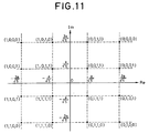
- the 16-value QAM baseband signal A is complex data having a real part (Re) and an imaginary part (Im). Correspondence between each signal point on a complex plane and a 4-bit input signal is shown in FIG. 11.
- TX transmitter
- the transmitter 107 performs the orthogonal modulation of the I and Q baseband signals, and outputs them from an antenna 115.
- a receiving side a high frequency signal transmitted from the transmitting side is received with an antenna 116, a receiver (RX) 108 performs an orthogonal demodulation to generate a baseband signal (I, Q) D.
- a serial/parallel converter (S/P) 109 samples this signal at the rate of 7.68 Msps respectively, and generates a parallel signal E consisting of 512 sets of I (real part) and Q (imaginary part) signals.
- FFT discrete Fourier transformer
- This data F expresses a signal point of each corresponding sub carrier on a complex plane.
- a corresponding 4-bit data (in the case of a 16-value QAM) is reproduced from this signal point, and is decoded into the original signal Y and outputted with a parallel/serial converter (P/S) 112.
- P/S parallel/serial converter
- the bit rate is transmitted in the OFDM at a very high-speed, for example, 30.72 Mbps. This is divided into many subcarriers and then transmitted.
- a symbol rate per sub carrier becomes only 15 ksps.
- the duration per one symbol is about 67 ⁇ sec, and this is a sufficiently large value (this is equivalent to 20 km) in comparison with the path difference of a usual multi-path. Therefore, the OFDM system has powerful resistance to multi-path transmission.
- the OFDM system is now planned with premising the utilization of each single unit such as digital television broadcast and high-speed wireless LAN equipment.
- each single unit such as digital television broadcast and high-speed wireless LAN equipment.
- the OFDM system has a feature of being essentially strong on the multi-path transmission, this feature is attractive also in other mobile communications.
- the plural kinds of communication signals have different bit rates respectively, and their necessary transmission quality (QoS: Quality of Service) are different according to informational types.
- An object of the present invention is to solve the above-described problems, and to provide an orthogonal frequency division multiplex modem circuit which can multiplex signals, whose bit rates and QoS are different from one another, and can transmit the signals via one OFDM line.
- An orthogonal frequency division multiplex modem circuit is an orthogonal frequency division multiplex modem circuit that uses a plurality of subcarriers for communication, and transmits and receives a plurality of communication channels.
- each of the plurality of sub carrier groups into which the plurality of subcarriers is divided is assigned to each of the plurality of communication channels.
- the orthogonal frequency division multiplex modem circuit provides a method for multiplexing and transmitting a plurality of communication channels whose bit rates and QoS (Quality of Service) are different from one another, via one OFDM (Orthogonal Frequency Division Multiplex) line.
- OFDM Orthogonal Frequency Division Multiplex
- a first orthogonal frequency division multiplex modem circuit is characterized in performing communications with using a plurality of subcarriers, dividing the plurality of subcarriers into a plurality of groups in an OFDM system which transmits and receives a plurality of communication channels, and assigning the sub carrier groups to the plurality of communication channels respectively.
- a second orthogonal frequency division multiplex modem circuit is characterized in that the assignment of sub carrier groups to respective communication channel is adaptively performed.
- a third orthogonal frequency division multiplex modem circuit according to the present invention is characterized in that a modulation system given to each of the sub carrier groups is changed according to the QoS (Quality of Service) needed for a corresponding communication channel.
- QoS Quality of Service
- a fourth orthogonal frequency division multiplex modem circuit is characterized in that means for randomizing the alignment of the respective subcarriers on a frequency axis is included in a transmitting side, and that means for de-randomizing the alignment is included in a receiving side.
- a fifth orthogonal frequency division multiplex modem circuit according to the present invention is characterized in that all subcarriers are assigned to a single channel as required, while communication of other channels is stopped.
- a sixth orthogonal frequency division multiplex modem circuit is characterized in that the changeable modulation system that is described above uses phase modulation such as BPSK (Binary Phase Shift Keying), QPSK (Quadrature Phase Shift Keying), and QAM (Quadrature Amplitude Modulation), and a symbol point on a phase plane is changed according to the QoS.
- phase modulation such as BPSK (Binary Phase Shift Keying), QPSK (Quadrature Phase Shift Keying), and QAM (Quadrature Amplitude Modulation
- a seventh orthogonal frequency division multiplex modem circuit is characterized in that, since it is desirable for the transmitted power of each sub carrier to be uniform, a peak value of each modulation symbol is determined so that the transmission power of the respective subcarriers may become the same irrespective of the modulation system.
- An eighth orthogonal frequency division multiplex modem circuit is characterized in that the processing for randomizing positions of respective subcarriers is updated at every symbol as means for preventing the suppression of a specific sub carrier caused by frequency-selective fading.
- a ninth orthogonal frequency division multiplex modem circuit is characterized in that means for determining a randomization pattern at every symbol and transmitting the randomization pattern to the receiving side at every symbol are included in the transmitting side, and means for synchronizing transmission and reception of the randomization pattern are included.
- a tenth orthogonal frequency division multiplex modem circuit is characterized in that the orthogonal frequency division multiplex modem circuit comprises means for determining a randomization pattern at symbol and transmitting the randomization pattern to the receiving side at every symbol are included in the transmitting side, and that a predetermined communication channel and a sub carrier corresponding to it are assigned as the means for synchronizing transmission and reception of the randomization pattern.
- An eleventh orthogonal frequency division multiplex modem circuit is characterized in that a predetermined communication channel and a sub carrier corresponding thereto is excluded from randomization process.
- the orthogonal frequency division multiplex modem circuits of the present invention can transmit communication channels whose bit rates and QoS are different from one another with using one OFDM line.
- FIG. 1 is a block diagram showing the structure of an orthogonal frequency division multiplexmodem circuit according to an embodiment of the present invention.
- the orthogonal frequency division multiplex modem circuit according to this embodiment of the present invention comprises a transmitting side consisting of serial/parallel converters (S/P) 101,102, and 103 , a randomizer 104, a discrete inverse Fourier transformer (IFFT) 105, a parallel/serial converter (P/S) 106, and a transmitter (TX) 107, and a receiving side consisting of a receiver (RX) 108, a serial/parallel converter (S/P) 109, a discrete Fourier transformer (FFT) 110, a de-randomizer 111, and parallel/serial converters (P/S) 112, 113, and 114.
- S/P serial/parallel converters
- FFT discrete Fourier transformer
- FIG. 2 is a block diagram showing a structural example of the serial/parallel converter 101 shown in FIG. 1.
- the serial/parallel converter 101 consists of a shift register 601 and 16-value QAM (Quadrature Amplitude Modulation) generating circuits 602, 603, 604, and 605.
- QAM Quadrature Amplitude Modulation
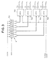
- FIG. 3 is a block diagram showing a structural example of the serial/parallel converter 102 shown in FIG. 1.
- the serial/parallel converter 102 consists of a shift register 701 and QPSK (Quadrature Phase Shift Keying) generating circuits 702, 703, 704, and 705.
- QPSK Quadrature Phase Shift Keying
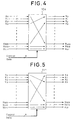
- FIG. 4 is a drawing for explaining the randomizer 104 shown in FIG. 1
- FIG. 5 is a drawing for explaining the de-randomizer 111 shown in FIG. 1.
- FIG. 6 is a time chart showing the operation of the serial/parallel converter 101 shown in FIG. 2
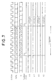
- FIG. 7 is a time chart showing the operation of the serial/parallel converter 102 shown in FIG. 3.
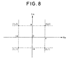
- FIG. 8 is a graph showing symbol points on a complex plane.
- the orthogonal frequency division multiplex modem circuit according to this embodiment of the present invention has a plurality of data inputs X1, X2, ..., Xn in the transmitting side, and has a plurality of data outputs Y1, Y2, ..., Yn, corresponding thereto, also in the receiving side.
- the input signals X1, X2, ..., Xn are converted into a complex parallel signal A with the serial/parallel converters 101, 102, and 103 respectively.
- the input signal X1 is inputted at the bit rate of 240 kbps. If the QoS of the input signal X1 is a middle degree, four subcarriers are assigned, and an output of the serial/parallel converter 101 becomes four complex numbers (it corresponded to four subcarriers) at 15 ksps in the case that a modulation system is the 16-value QAM,
- serial/parallel converter 101 generating the 16-value QAM, as shown in FIG. 2, data is inputted into the shift register 601 driven by a clock having a frequency equal to the data rate.
- the 4-bit parallel outputs of the shift register 601 are grouped together, and then inputted into the 16-value QAM generating circuits 602,603,604,605 respectively to be incorporated with a clock (Symbol CLOCK) equal to the symbol rate.
- FIG. 6 shows a timing chart of the operation.
- serial/parallel converter 102 In the serial/parallel converter 102, as shown in FIG. 3, data is inputted into the shift register 701 driven with a clock having a frequency equal to a data rate.
- a parallel output of the shift register 701 is set every 2 bits, and is inputted into the QPSK generating circuits 702, 703, 704, and 705 respectively to be incorporated with a clock (Symbol CLOCK) equal to a symbol rate.
- a symbol point on a complex plane as shown in FIG. 8 is chosen, and each real part (Re) and an imaginary part (Im) are outputted.
- a timing chart of the operation is shown in FIG. 7.
- a sub carrier is assigned.
- an output of the serial/parallel converter 103 also becomes one complex number at 15 ksps (it corresponds to one sub carrier).
- an adequate modulation system and the number of subcarriers to be assigned can be determined from the bit rate and QoS, and the symbol rates of all subcarriers can be set to the same rate, 15 kHz.
- subcarriers and a modulation system are assigned for every communication channel, and 512 complex data symbols (at the symbol rate of 15 kbps) in total are obtained.
- the sub carrier can be made not to be modulated, that is, to be a complex number (0+j0).
- the sequence of the alignment of 512 pieces of parallel complex data obtained in this manner is replaced by the randomizer 104.
- This operation is performed per symbol.
- the randomizer 104 replaces the sequence at every symbol with a control signal (for example, 8 bits). If the control signal is 8 bits, 256 kinds of replacement can be performed.
- a control signal for example, 8 bits. If the control signal is 8 bits, 256 kinds of replacement can be performed.
- FIG. 4 although the input signals X510 and X511 are connected to Y510 and Y511 as it is, this supposes the control channel.
- the control channel transmits symbol synchronization and information about a randomization pattern to the receiving side. Hence, it facilitates an initial access to transmit it as it is without performing randomization.
- the discrete inverse Fourier transformer 105 processes 512 pieces of randomized parallel complex data A' to obtain 512 sets of I and Q parallel data B.
- the parallel/serial converter 106 converts this result into a serial signal C.
- the transmitter 107 performs the orthogonal modulation of the I and Q baseband signals, and outputs them from the antenna 115.
- the receiving side receives the high frequency signal transmitted from the transmitting side with the antenna 116, and performs orthogonal demodulation with the receiver 108 to generate a baseband signal (I and Q) D.
- the receiving side samples this at the rate of 7.68 Msps with the serial/parallel converter 109 respectively to generate a parallel signal E that consists of 512 sets of I (real part) and Q (imaginary part) signals.
- the discrete Fourier transformer 110 receives this signal to output 512 complex numbers.
- These data F' express signal points of corresponding subcarriers on a complex plane.
- the de-randomizer 111 receives this result, and restores the sequence of the subcarriers that is changed in the randomizer 104.
- the de-randomizer 111 replaces the sequence per symbol with the control signal (for example, 8 bits), as shown in FIG. 5. If the control signal is 8 bits, 256 kinds of replacement can be performed.
- the input signals Y510 and Y511 are connected to X510 and X511 as it is, this supposes the control channel.
- the control channel transmits symbol synchronization and information about a randomization pattern to the receiving side. Hence, it facilitates an initial access to transmit them as they are without performing randomization.
- the result F of the de-randomization expresses signal points of corresponding subcarriers on a complex plane.
- the corresponding bit data is restored from these signal points and the modulation systems of respective subcarriers, and is decoded and outputted to the original signals Y1 and Y2, ..., Yn with the parallel/serial converters 112,113, and 114.
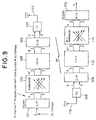
- FIG. 9 is a block diagram showing the structure of an orthogonal frequency division multiplex modem circuit according to another embodiment of the present invention.
- the structure of the orthogonal frequency division multiplex modem circuit with a single channel is shown.
- the orthogonal frequency division multiplex modem circuit comprises a transmitting side consisting of a serial/parallel converter (S/P) 101, a randomizer 104, a discrete inverse Fourier transformer (IFFT) 105, a parallel/serial converter (P/S) 106, and a transmitter (TX) 107, and a receiving side consisting of a receiver (RX) 108, a serial/parallel converter (S/P) 109, a discrete Fourier transformer (FFT) 110, a de-randomizer 111, and a parallel/serial converter (P/S) 112.
- S/P serial/parallel converter
- IFFT discrete inverse Fourier transformer
- P/S parallel/serial converter
- TX transmitter
- RX receiver
- S/P serial/parallel converter
- FFT discrete Fourier transformer
- de-randomizer 111 a de-randomizer
- P/S parallel/serial converter
- the orthogonal frequency division multiplex modem circuit according to the embodiment of the present invention is primarily intended to transmit a plurality of communication channels with different bit rates and QoS via one OFDM line. However, depending on the case, only one communication channel can be passed preferentially.
- the orthogonal frequency division multiplex modem circuit according to this embodiment of the present invention has the above-described structure.
- the present invention includes also adaptively determining the assignment of subcarriers and modulation systems according to the priorities, bit rates, and QoS of communication channels.
- the present invention also includes making the mean signal power of all subcarriers uniform by adjusting peak values of symbols.
- the present invention has an advantage that, the orthogonal frequency division multiplex modem circuit which uses a plurality of subcarriers for communication, and transmits and receives a plurality of communication channels can multiplex and transmit signals, whose bit rates and QoS are different from one another, via one OFDM line by assigning each of sub carrier groups, into which the plurality of subcarriers is divided, to each of the plurality of communication channels.
Landscapes
- Engineering & Computer Science (AREA)
- Signal Processing (AREA)
- Computer Networks & Wireless Communication (AREA)
- Quality & Reliability (AREA)
- Digital Transmission Methods That Use Modulated Carrier Waves (AREA)
- Mobile Radio Communication Systems (AREA)
Abstract
Description
Claims (11)
- An orthogonal frequency division multiplex modem circuit which uses a plurality of subcarriers for communication, and transmits and receives a plurality of communication channels, wherein each of the plurality of sub carrier groups into which the plurality of subcarriers are divided is assigned to each of the plurality of communication channels.
- The orthogonal frequency division multiplex modem circuit according to claim 1, wherein the assignment of sub carrier groups to the respective communication channels is performed in different manners.
- The orthogonal frequency division multiplex modem circuit according to claim 1, wherein a modulation system given to each of the sub carrier groups is changed according to QoS (Quality of Service) needed for a corresponding communication channel.
- The orthogonal frequency division multiplex modem circuit according to claim 1, wherein means for randomizing alignment of the respective subcarriers on a frequency axis is included in a transmitting side, and means for de-randomizing a signal where the alignment is randomized is included in a receiving side.
- The orthogonal frequency division multiplex modem circuit according to claim 2, wherein all subcarriers are assigned to a single channel as required, while communication of other channels is stopped.
- The orthogonal frequency division multiplex modem circuit according to claim 3, wherein the changeable modulation system uses at least any one of BPSK (Binary Phase Shift Keying), QPSK (Quadrature Phase Shift Keying), and QAM (Quadrature Amplitude Modulation), and a symbol point on a phase plane is changed according to the QoS.
- The orthogonal frequency division multiplex modem circuit according to claim 3, wherein peak values of modulation symbols are determined so that transmission power of the respective subcarriers becomes the same irrespective of the modulation systems.
- The orthogonal frequency division multiplex modem circuit according to claim 4, wherein the processing for randomizing positions of the respective subcarriers is updated at every symbol.
- The orthogonal frequency division multiplex modem circuit according to claim 8, wherein means for determining the randomization pattern at every symbol and transmitting the randomization pattern at every symbol to the receiving side is included in the transmitting side, and means for synchronizing transmission and reception of the randomization pattern is included.
- The orthogonal frequency division multiplex modem circuit according to claim 9, wherein a predetermined communication channel and a sub carrier corresponding thereto are assigned as the means for synchronizing transmission and reception of the randomization pattern.
- The orthogonal frequency division multiplex modem circuit according to claim 10, wherein the predetermined communication channel and the sub carrier corresponding thereto are excluded from the randomization process.
Priority Applications (1)
| Application Number | Priority Date | Filing Date | Title |
|---|---|---|---|
| EP07090002.2A EP1773015B1 (en) | 2000-06-14 | 2001-06-12 | Orthogonal frequency division multiplex modem circuit |
Applications Claiming Priority (2)
| Application Number | Priority Date | Filing Date | Title |
|---|---|---|---|
| JP2000177711 | 2000-06-14 | ||
| JP2000177711A JP2001358692A (en) | 2000-06-14 | 2000-06-14 | Orthogonal frequency-division multiplex modulating and demodulating circuit |
Related Child Applications (1)
| Application Number | Title | Priority Date | Filing Date |
|---|---|---|---|
| EP07090002.2A Division EP1773015B1 (en) | 2000-06-14 | 2001-06-12 | Orthogonal frequency division multiplex modem circuit |
Publications (3)
| Publication Number | Publication Date |
|---|---|
| EP1164740A2 true EP1164740A2 (en) | 2001-12-19 |
| EP1164740A3 EP1164740A3 (en) | 2003-12-17 |
| EP1164740B1 EP1164740B1 (en) | 2007-08-15 |
Family
ID=18679260
Family Applications (2)
| Application Number | Title | Priority Date | Filing Date |
|---|---|---|---|
| EP01250209A Expired - Lifetime EP1164740B1 (en) | 2000-06-14 | 2001-06-12 | Arrangement for multicarrier modulation and multiplexing |
| EP07090002.2A Expired - Lifetime EP1773015B1 (en) | 2000-06-14 | 2001-06-12 | Orthogonal frequency division multiplex modem circuit |
Family Applications After (1)
| Application Number | Title | Priority Date | Filing Date |
|---|---|---|---|
| EP07090002.2A Expired - Lifetime EP1773015B1 (en) | 2000-06-14 | 2001-06-12 | Orthogonal frequency division multiplex modem circuit |
Country Status (6)
| Country | Link |
|---|---|
| US (3) | US7099268B2 (en) |
| EP (2) | EP1164740B1 (en) |
| JP (1) | JP2001358692A (en) |
| KR (1) | KR100437306B1 (en) |
| CN (2) | CN1855908B (en) |
| DE (1) | DE60129884T2 (en) |
Cited By (3)
| Publication number | Priority date | Publication date | Assignee | Title |
|---|---|---|---|---|
| WO2005125139A1 (en) * | 2004-06-16 | 2005-12-29 | Samsung Electronics Co., Ltd. | Method for transmitting/receiving data in mobile communication systems using an ofdma scheme |
| EP2827514A4 (en) * | 2012-03-16 | 2015-05-20 | Fujitsu Ltd | LIGHT TRANSMISSION APPARATUS AND LIGHT TRANSMISSION METHOD |
| CN111464478A (en) * | 2019-01-21 | 2020-07-28 | 华为技术有限公司 | A kind of signal transmission and reception method and equipment |
Families Citing this family (59)
| Publication number | Priority date | Publication date | Assignee | Title |
|---|---|---|---|---|
| US8670390B2 (en) | 2000-11-22 | 2014-03-11 | Genghiscomm Holdings, LLC | Cooperative beam-forming in wireless networks |
| US9819449B2 (en) | 2002-05-14 | 2017-11-14 | Genghiscomm Holdings, LLC | Cooperative subspace demultiplexing in content delivery networks |
| US10931338B2 (en) | 2001-04-26 | 2021-02-23 | Genghiscomm Holdings, LLC | Coordinated multipoint systems |
| US10355720B2 (en) | 2001-04-26 | 2019-07-16 | Genghiscomm Holdings, LLC | Distributed software-defined radio |
| FR2825861A1 (en) * | 2001-06-06 | 2002-12-13 | St Microelectronics Sa | FREQUENCY ALLOCATION IN ORTHOGONAL MULTIPORTER MODULATION |
| US20040218521A1 (en) * | 2001-08-01 | 2004-11-04 | Edgar Bolinth | Method for data communication between a single-carrier system and a multi-carrier system |
| US7012883B2 (en) * | 2001-11-21 | 2006-03-14 | Qualcomm Incorporated | Rate selection for an OFDM system |
| JP3548162B2 (en) * | 2002-02-15 | 2004-07-28 | 松下電器産業株式会社 | Transmission device |
| JP3963737B2 (en) | 2002-02-28 | 2007-08-22 | 松下電器産業株式会社 | Multi-carrier signal generation method, radio transmission apparatus, and radio reception apparatus |
| KR20030094909A (en) * | 2002-06-10 | 2003-12-18 | 삼성전자주식회사 | A method for OFDM multi-carrier modulating a digital broadcasting signal using the TDS-OFDM transmitter |
| US10644916B1 (en) | 2002-05-14 | 2020-05-05 | Genghiscomm Holdings, LLC | Spreading and precoding in OFDM |
| US10142082B1 (en) | 2002-05-14 | 2018-11-27 | Genghiscomm Holdings, LLC | Pre-coding in OFDM |
| US10200227B2 (en) | 2002-05-14 | 2019-02-05 | Genghiscomm Holdings, LLC | Pre-coding in multi-user MIMO |
| US9628231B2 (en) | 2002-05-14 | 2017-04-18 | Genghiscomm Holdings, LLC | Spreading and precoding in OFDM |
| KR100478539B1 (en) * | 2002-07-11 | 2005-03-24 | 김정환 | Monitoring method using communication network |
| WO2004008671A1 (en) * | 2002-07-16 | 2004-01-22 | Matsushita Electric Industrial Co., Ltd. | Communicating method, transmitting device using the same, and receiving device using the same |
| GB2391431A (en) * | 2002-07-30 | 2004-02-04 | Fujitsu Ltd | Adaptive modulation and coding method |
| KR100552680B1 (en) * | 2003-02-17 | 2006-02-20 | 삼성전자주식회사 | Method for reducing PRA in multi-antenna OMD communication system and multi-antenna OMD communication system using same |
| US7394858B2 (en) * | 2003-08-08 | 2008-07-01 | Intel Corporation | Systems and methods for adaptive bit loading in a multiple antenna orthogonal frequency division multiplexed communication system |
| KR100539925B1 (en) * | 2003-08-22 | 2005-12-28 | 삼성전자주식회사 | Apparatus and method for sub-carrier alocation in ofdm system |
| KR100876757B1 (en) | 2003-10-31 | 2009-01-07 | 삼성전자주식회사 | Subchannel Configuration System and Method in Communication System |
| US8204149B2 (en) | 2003-12-17 | 2012-06-19 | Qualcomm Incorporated | Spatial spreading in a multi-antenna communication system |
| US7336746B2 (en) | 2004-12-09 | 2008-02-26 | Qualcomm Incorporated | Data transmission with spatial spreading in a MIMO communication system |
| US8169889B2 (en) | 2004-02-18 | 2012-05-01 | Qualcomm Incorporated | Transmit diversity and spatial spreading for an OFDM-based multi-antenna communication system |
| KR100842588B1 (en) | 2004-03-12 | 2008-07-01 | 삼성전자주식회사 | Method and apparatus for subcarrier allocation in broadband wireless communication system using multicarrier transmission |
| US8923785B2 (en) | 2004-05-07 | 2014-12-30 | Qualcomm Incorporated | Continuous beamforming for a MIMO-OFDM system |
| US8285226B2 (en) | 2004-05-07 | 2012-10-09 | Qualcomm Incorporated | Steering diversity for an OFDM-based multi-antenna communication system |
| US7978649B2 (en) | 2004-07-15 | 2011-07-12 | Qualcomm, Incorporated | Unified MIMO transmission and reception |
| US11184037B1 (en) | 2004-08-02 | 2021-11-23 | Genghiscomm Holdings, LLC | Demodulating and decoding carrier interferometry signals |
| US11552737B1 (en) | 2004-08-02 | 2023-01-10 | Genghiscomm Holdings, LLC | Cooperative MIMO |
| US11431386B1 (en) | 2004-08-02 | 2022-08-30 | Genghiscomm Holdings, LLC | Transmit pre-coding |
| KR100718592B1 (en) * | 2005-12-31 | 2007-05-17 | 포스데이타 주식회사 | Channel Estimation Apparatus and Method for Communication System Supporting OPDM / OPDMA System |
| KR101227245B1 (en) * | 2006-04-07 | 2013-01-28 | 재단법인서울대학교산학협력재단 | Apparatus and method for transmitting/receiving a signal in a beam forming/multiple input multiple output-orthogonal frequency division multiplexing communication system |
| US8543070B2 (en) | 2006-04-24 | 2013-09-24 | Qualcomm Incorporated | Reduced complexity beam-steered MIMO OFDM system |
| EP1858208A1 (en) * | 2006-05-19 | 2007-11-21 | Nokia Siemens Networks Gmbh & Co. Kg | Method and node for providing a quality of service support in multihop communication systems |
| US8290089B2 (en) | 2006-05-22 | 2012-10-16 | Qualcomm Incorporated | Derivation and feedback of transmit steering matrix |
| EP1912374A1 (en) * | 2006-10-10 | 2008-04-16 | Nokia Siemens Networks Gmbh & Co. Kg | Data transmission in a multiuser OFDM system with adaptive modulation |
| KR100801290B1 (en) * | 2006-11-16 | 2008-02-05 | 한국전자통신연구원 | Demodulation Device and Method for Orthogonal Frequency Division Multiple Access Communication System |
| US7852745B2 (en) | 2007-03-02 | 2010-12-14 | Signalink Technologies Inc. | Non-orthogonal frequency-division multiplexed communication through a non-linear transmission medium |
| JP4823107B2 (en) * | 2007-03-09 | 2011-11-24 | 株式会社日立製作所 | OFDM modulator |
| KR100901692B1 (en) * | 2007-03-27 | 2009-06-08 | 한국전자통신연구원 | Multimode transceiver in low speed wireless personal communication network and method thereof |
| JP2008252315A (en) * | 2007-03-29 | 2008-10-16 | Kddi Corp | Wireless device |
| JP5115369B2 (en) | 2008-07-09 | 2013-01-09 | 富士通株式会社 | Base station apparatus, communication system, and channel allocation method |
| US9021341B1 (en) * | 2010-06-16 | 2015-04-28 | Marvell International Ltd. | LDPC coding in a communication system |
| US8565342B2 (en) * | 2010-06-22 | 2013-10-22 | Sony Corporation | Power amplification apparatus, OFDM modulation apparatus, wireless transmission apparatus, and distortion reduction method for power amplification apparatus |
| US9294216B2 (en) * | 2011-03-03 | 2016-03-22 | Ofidium Pty. Ltd. | Optical OFDM transmission |
| TW201445989A (en) * | 2013-05-30 | 2014-12-01 | Hon Hai Prec Ind Co Ltd | System and method for encoding and decoding data |
| CN103647742B (en) * | 2013-12-25 | 2017-09-08 | 上海贝岭股份有限公司 | The communication means and equipment of power line carrier ofdm system |
| US12224860B1 (en) | 2014-01-30 | 2025-02-11 | Genghiscomm Holdings, LLC | Linear coding in decentralized networks |
| EP3119051B1 (en) * | 2014-03-13 | 2019-11-20 | Mitsubishi Electric Corporation | Likelihood generation device and method therefor |
| CN108770382B (en) | 2015-09-07 | 2022-01-14 | 凝聚技术公司 | Multiple access method using orthogonal time frequency space modulation |
| US10243773B1 (en) | 2017-06-30 | 2019-03-26 | Genghiscomm Holdings, LLC | Efficient peak-to-average-power reduction for OFDM and MIMO-OFDM |
| US10637705B1 (en) | 2017-05-25 | 2020-04-28 | Genghiscomm Holdings, LLC | Peak-to-average-power reduction for OFDM multiple access |
| US11917604B2 (en) | 2019-01-25 | 2024-02-27 | Tybalt, Llc | Orthogonal multiple access and non-orthogonal multiple access |
| US12206535B1 (en) | 2018-06-17 | 2025-01-21 | Tybalt, Llc | Artificial neural networks in wireless communication systems |
| US11343823B2 (en) | 2020-08-16 | 2022-05-24 | Tybalt, Llc | Orthogonal multiple access and non-orthogonal multiple access |
| US10560097B1 (en) * | 2018-09-28 | 2020-02-11 | Teletrx Co. | High-speed 4:1 multiplexer for voltage-mode transmitter with automatic phase alignment technique |
| EP3915236A4 (en) | 2019-01-25 | 2023-05-24 | Genghiscomm Holdings, LLC | ORTHOGONAL MULTIPLE ACCESS, AND NON-ORTHOGONAL MULTIPLE ACCESS |
| WO2020242898A1 (en) | 2019-05-26 | 2020-12-03 | Genghiscomm Holdings, LLC | Non-orthogonal multiple access |
Family Cites Families (37)
| Publication number | Priority date | Publication date | Assignee | Title |
|---|---|---|---|---|
| ATE139660T1 (en) * | 1990-03-30 | 1996-07-15 | Digi Media Vision Ltd | TRANSMIT AND RECEIVE IN AN INTERFERENTIAL INTERFERENCE ENVIRONMENT |
| US5555268A (en) * | 1994-01-24 | 1996-09-10 | Fattouche; Michel | Multicode direct sequence spread spectrum |
| US6334219B1 (en) | 1994-09-26 | 2001-12-25 | Adc Telecommunications Inc. | Channel selection for a hybrid fiber coax network |
| JP3145003B2 (en) * | 1995-03-23 | 2001-03-12 | 株式会社東芝 | Orthogonal frequency division multiplexing transmission system and transmitter and receiver thereof |
| GB9510127D0 (en) * | 1995-05-20 | 1995-08-02 | West End System Corp | CATV Data transmission system |
| JP3597602B2 (en) | 1995-05-31 | 2004-12-08 | 株式会社東芝 | Wireless communication device |
| DE69528974T2 (en) * | 1995-07-11 | 2003-08-28 | Alcatel, Paris | Capacity allocation in a multi-carrier system |
| US5790516A (en) * | 1995-07-14 | 1998-08-04 | Telefonaktiebolaget Lm Ericsson | Pulse shaping for data transmission in an orthogonal frequency division multiplexed system |
| US6072779A (en) | 1997-06-12 | 2000-06-06 | Aware, Inc. | Adaptive allocation for variable bandwidth multicarrier communication |
| US6192068B1 (en) * | 1996-10-03 | 2001-02-20 | Wi-Lan Inc. | Multicode spread spectrum communications system |
| KR100204585B1 (en) * | 1996-12-14 | 1999-06-15 | 정선종 | IFF / FTF Block and Timing Synchronization Method Applicable to OSF / CMD |
| JP3535344B2 (en) * | 1997-05-30 | 2004-06-07 | 松下電器産業株式会社 | Multicarrier transmission method, data transmission device, mobile station device, and base station device |
| US6314102B1 (en) * | 1997-07-10 | 2001-11-06 | Alcatel | Telecommunications system for providing both narrowband and broadband services to subscribers |
| JP3797510B2 (en) * | 1997-07-16 | 2006-07-19 | ソニー株式会社 | COMMUNICATION METHOD, TRANSMISSION DEVICE, RECEPTION DEVICE, AND CELLULAR RADIO COMMUNICATION SYSTEM |
| US6038450A (en) * | 1997-09-12 | 2000-03-14 | Lucent Technologies, Inc. | Soft handover system for a multiple sub-carrier communication system and method thereof |
| EP0912023A1 (en) * | 1997-10-27 | 1999-04-28 | Alcatel | Demodulation and equalisation of multicarrier signals |
| EP0915586B1 (en) * | 1997-11-07 | 2005-05-18 | Sony International (Europe) GmbH | Multicarrier transmission, compatible with the existing GSM system |
| JP3097634B2 (en) * | 1997-11-07 | 2000-10-10 | 日本電信電話株式会社 | OFDM modulation / demodulation circuit |
| GB2332603B (en) * | 1997-12-22 | 2000-07-19 | Lsi Logic Corp | Improvements relating to multidirectional communication systems |
| GB2332602B (en) * | 1997-12-22 | 2000-03-08 | Lsi Logic Corp | Improvements relating to multidirectional communication systems |
| EP0930752A3 (en) | 1998-01-14 | 1999-10-20 | Motorola, Inc. | Method for allocating data and power in a discrete multitone communication system |
| JPH11266224A (en) | 1998-03-18 | 1999-09-28 | Nippon Telegr & Teleph Corp <Ntt> | Orthogonal frequency multiplex communication equipment |
| US6108810A (en) * | 1998-03-27 | 2000-08-22 | Usa Digital Radio, Inc. | Digital audio broadcasting method using puncturable convolutional code |
| US6445750B1 (en) * | 1998-04-22 | 2002-09-03 | Lucent Technologies Inc. | Technique for communicating digitally modulated signals over an amplitude-modulation frequency band |
| JP3515690B2 (en) * | 1998-06-02 | 2004-04-05 | 松下電器産業株式会社 | OFDMA signal transmission apparatus and method |
| US6246713B1 (en) * | 1998-06-08 | 2001-06-12 | Telefonaktiebolaget Lm Ericsson (Publ) | Frequency-hopping in a bandwidth-on-demand system |
| GB2339514A (en) * | 1998-07-11 | 2000-01-26 | Motorola Ltd | Cellular communication system with reduced power variation |
| JP2000092009A (en) | 1998-07-13 | 2000-03-31 | Sony Corp | Communication method, transmitter and receiver |
| JP2000115116A (en) * | 1998-10-07 | 2000-04-21 | Nippon Columbia Co Ltd | Orthogonal frequency division multiplex signal generator, orthogonal frequency division multiplex signal generation method and communication equipment |
| US7039120B1 (en) * | 1998-11-30 | 2006-05-02 | Canon Kabushiki Kaisha | Device and method for the dynamic allocation of frequencies for multicarrier modulation systems |
| JP2000252951A (en) * | 1999-03-01 | 2000-09-14 | Sony Corp | Synchronous signal detection method and wireless communication device |
| JP2000287086A (en) * | 1999-03-31 | 2000-10-13 | Minolta Co Ltd | Image processor |
| JP2001036499A (en) * | 1999-07-23 | 2001-02-09 | Fujitsu Ltd | Communication band setting method and communication device |
| US6442129B1 (en) * | 1999-12-06 | 2002-08-27 | Intellon Corporation | Enhanced channel estimation |
| US6397368B1 (en) * | 1999-12-06 | 2002-05-28 | Intellon Corporation | Forward error correction with channel adaptation |
| US6628673B1 (en) * | 1999-12-29 | 2003-09-30 | Atheros Communications, Inc. | Scalable communication system using overlaid signals and multi-carrier frequency communication |
| US6807146B1 (en) * | 2000-04-21 | 2004-10-19 | Atheros Communications, Inc. | Protocols for scalable communication system using overland signals and multi-carrier frequency communication |
-
2000
- 2000-06-14 JP JP2000177711A patent/JP2001358692A/en active Pending
-
2001
- 2001-06-12 EP EP01250209A patent/EP1164740B1/en not_active Expired - Lifetime
- 2001-06-12 US US09/879,323 patent/US7099268B2/en not_active Expired - Lifetime
- 2001-06-12 DE DE60129884T patent/DE60129884T2/en not_active Expired - Lifetime
- 2001-06-12 EP EP07090002.2A patent/EP1773015B1/en not_active Expired - Lifetime
- 2001-06-13 CN CN2006100817569A patent/CN1855908B/en not_active Expired - Lifetime
- 2001-06-13 CN CNB011187883A patent/CN1284316C/en not_active Expired - Lifetime
- 2001-06-13 KR KR10-2001-0033186A patent/KR100437306B1/en not_active Expired - Lifetime
-
2006
- 2006-05-25 US US11/441,257 patent/US7843803B2/en not_active Expired - Lifetime
-
2010
- 2010-10-27 US US12/913,266 patent/US8335153B2/en not_active Expired - Lifetime
Cited By (8)
| Publication number | Priority date | Publication date | Assignee | Title |
|---|---|---|---|---|
| WO2005125139A1 (en) * | 2004-06-16 | 2005-12-29 | Samsung Electronics Co., Ltd. | Method for transmitting/receiving data in mobile communication systems using an ofdma scheme |
| US7505397B2 (en) | 2004-06-16 | 2009-03-17 | Samsung Electronics Co., Ltd | Method for transmitting/receiving data in mobile communication systems using an OFDMA scheme |
| CN1998211B (en) * | 2004-06-16 | 2010-05-12 | 三星电子株式会社 | Method for transmitting/receiving data in mobile communication system using orthogonal frequency division multiple access scheme |
| EP2827514A4 (en) * | 2012-03-16 | 2015-05-20 | Fujitsu Ltd | LIGHT TRANSMISSION APPARATUS AND LIGHT TRANSMISSION METHOD |
| US9749055B2 (en) | 2012-03-16 | 2017-08-29 | Fujitsu Limited | Optical transmitter and optical transmission method |
| CN111464478A (en) * | 2019-01-21 | 2020-07-28 | 华为技术有限公司 | A kind of signal transmission and reception method and equipment |
| CN111464478B (en) * | 2019-01-21 | 2023-04-07 | 华为技术有限公司 | Signal sending and receiving method and equipment |
| US11956178B2 (en) | 2019-01-21 | 2024-04-09 | Huawei Technologies Co., Ltd. | Signal sending method, signal receiving method, and device |
Also Published As
| Publication number | Publication date |
|---|---|
| CN1855908A (en) | 2006-11-01 |
| EP1773015A1 (en) | 2007-04-11 |
| CN1284316C (en) | 2006-11-08 |
| US20010053124A1 (en) | 2001-12-20 |
| US7843803B2 (en) | 2010-11-30 |
| CN1855908B (en) | 2011-04-20 |
| EP1164740A3 (en) | 2003-12-17 |
| KR100437306B1 (en) | 2004-06-25 |
| CN1329406A (en) | 2002-01-02 |
| KR20010112656A (en) | 2001-12-20 |
| EP1164740B1 (en) | 2007-08-15 |
| US20110038403A1 (en) | 2011-02-17 |
| US7099268B2 (en) | 2006-08-29 |
| US20060209673A1 (en) | 2006-09-21 |
| JP2001358692A (en) | 2001-12-26 |
| DE60129884D1 (en) | 2007-09-27 |
| DE60129884T2 (en) | 2008-04-30 |
| US8335153B2 (en) | 2012-12-18 |
| EP1773015B1 (en) | 2018-02-28 |
Similar Documents
| Publication | Publication Date | Title |
|---|---|---|
| US7099268B2 (en) | Orthogonal frequency division multiplex modem circuit | |
| US11147067B2 (en) | Communication radio transmitter | |
| EP1503534B1 (en) | Method and device for selecting subcarriers according to quality of service requirements in a multicarrier communications system | |
| EP2259532B1 (en) | Pilot frequency selection | |
| US7042957B1 (en) | Method and communication system for transmitting information with the aid of a multicarrier method | |
| CA2290596C (en) | System for the transmission of high-rate value-added services by terrestrial broadcasting | |
| JP3786129B2 (en) | Orthogonal frequency division multiplexing modulation / demodulation circuit | |
| JP2002261727A (en) | OFDM signal transmission equipment | |
| US7206278B2 (en) | Method and system for increasing the total amount of useful information (throughput) transmitted in a radiocommunication system |
Legal Events
| Date | Code | Title | Description |
|---|---|---|---|
| PUAI | Public reference made under article 153(3) epc to a published international application that has entered the european phase |
Free format text: ORIGINAL CODE: 0009012 |
|
| AK | Designated contracting states |
Kind code of ref document: A2 Designated state(s): AT BE CH CY DE DK ES FI FR GB GR IE IT LI LU MC NL PT SE TR |
|
| AX | Request for extension of the european patent |
Free format text: AL;LT;LV;MK;RO;SI |
|
| PUAL | Search report despatched |
Free format text: ORIGINAL CODE: 0009013 |
|
| RIC1 | Information provided on ipc code assigned before grant |
Ipc: 7H 04L 5/02 B Ipc: 7H 04L 5/06 A Ipc: 7H 04L 27/26 B |
|
| AK | Designated contracting states |
Kind code of ref document: A3 Designated state(s): AT BE CH CY DE DK ES FI FR GB GR IE IT LI LU MC NL PT SE TR |
|
| AX | Request for extension of the european patent |
Extension state: AL LT LV MK RO SI |
|
| 17P | Request for examination filed |
Effective date: 20040112 |
|
| AKX | Designation fees paid |
Designated state(s): DE GB |
|
| GRAP | Despatch of communication of intention to grant a patent |
Free format text: ORIGINAL CODE: EPIDOSNIGR1 |
|
| GRAS | Grant fee paid |
Free format text: ORIGINAL CODE: EPIDOSNIGR3 |
|
| GRAA | (expected) grant |
Free format text: ORIGINAL CODE: 0009210 |
|
| AK | Designated contracting states |
Kind code of ref document: B1 Designated state(s): DE GB |
|
| REG | Reference to a national code |
Ref country code: GB Ref legal event code: FG4D |
|
| REF | Corresponds to: |
Ref document number: 60129884 Country of ref document: DE Date of ref document: 20070927 Kind code of ref document: P |
|
| PLBE | No opposition filed within time limit |
Free format text: ORIGINAL CODE: 0009261 |
|
| STAA | Information on the status of an ep patent application or granted ep patent |
Free format text: STATUS: NO OPPOSITION FILED WITHIN TIME LIMIT |
|
| 26N | No opposition filed |
Effective date: 20080516 |
|
| REG | Reference to a national code |
Ref country code: GB Ref legal event code: 732E Free format text: REGISTERED BETWEEN 20141023 AND 20141029 |
|
| REG | Reference to a national code |
Ref country code: DE Ref legal event code: R082 Ref document number: 60129884 Country of ref document: DE Representative=s name: STORK BAMBERGER PATENTANWAELTE PARTMBB, DE Ref country code: DE Ref legal event code: R081 Ref document number: 60129884 Country of ref document: DE Owner name: LENOVO INNOVATIONS LIMITED, HK Free format text: FORMER OWNER: NEC CORP., TOKYO, JP Ref country code: DE Ref legal event code: R082 Ref document number: 60129884 Country of ref document: DE Representative=s name: KASTEL PATENTANWAELTE PARTG MBB, DE |
|
| REG | Reference to a national code |
Ref country code: DE Ref legal event code: R082 Ref document number: 60129884 Country of ref document: DE Representative=s name: KASTEL PATENTANWAELTE PARTG MBB, DE |
|
| PGFP | Annual fee paid to national office [announced via postgrant information from national office to epo] |
Ref country code: GB Payment date: 20200630 Year of fee payment: 20 |
|
| PGFP | Annual fee paid to national office [announced via postgrant information from national office to epo] |
Ref country code: DE Payment date: 20200630 Year of fee payment: 20 |
|
| REG | Reference to a national code |
Ref country code: DE Ref legal event code: R071 Ref document number: 60129884 Country of ref document: DE |
|
| REG | Reference to a national code |
Ref country code: GB Ref legal event code: PE20 Expiry date: 20210611 |
|
| PG25 | Lapsed in a contracting state [announced via postgrant information from national office to epo] |
Ref country code: GB Free format text: LAPSE BECAUSE OF EXPIRATION OF PROTECTION Effective date: 20210611 |