FIELD OF THE INVENTION
-
The invention relates to a method for fabricating a
semiconductor device, and especially to a method for
fabricating a semiconductor device in which etching by-products
deposited on side walls of an electrode in a dry etching process
can be removed effectively without dispersion of particles.
-
In recent years, a capacitor in which precious metal or
oxide thereof, such as Ir, Pt, or IrO2, is used as material of
an electrode thereof, and a microdevice, such as a dynamic
random access memory (DRAM) which is provided with the
capacitors using ferroelectric insulating layers, such as
strontium titanate layers (STO layers) or barium strontium
titanate layers (BTS layers), or a FRAM which uses the
aforementioned precious metal and the ferroelectric insulating
layers, such as zirconium lead titanate layers (PZT layers) or
strontium bithmuth tantalum oxide layers (Y1 layers), is
actively developed.
-
FIGs. 1A, 1B show a fine process of precious metal used
in the microdevice.
-
As shown in FIG.1A, a photo-resist 1 is formed on a
precious metal layer 2 formed of Pt or Ir, and deposited films
3 produced as etching by-products are deposited on both sides
of the photo-resist mask 1 and the precious metal layer 2. The
etching by-product 3 is formed in accordance with a following
process that Pt ions which are spattered from and re-deposited
on a Pt layer change into a by-product formed of Pt and Cl
mixtured compounds.
-
Next, an etching process for pattering the precious metal
layer 2 will be explained. After the photo-resist mask 1 having
a predetermined pattern is formed on a surface of the precious
metal layer 2, the precious metal layer is dry etched by a
halogenous gas, such as a mixture gas of Cl2 and Ar.
-
After the aforementioned etching process is over, the
photo-resist mask 1 which has become unnecessary is ashed and
stripped. A state that the resist 1 has been removed is shown
in FIG.1B.
-
Since the saturated vapor pressure of a halogenide of
precious metal is low, the deposited films formed of precious
metal and the halogenide thereof are stuck to the side walls
of the photo-resist mask 1 as the etching by-products 3 after
dry etching is over as shown in FIG.1A. Even when the resist
mask is ashed and stripped by oxygen plasma, the etching
by-product 3 is hard to remove, and remains as residue like a
fence. The etching by-product 3 must be removed by a physical
method such as scrub cleansing formerly, and a surface of the
semiconductor substrate is scrubbed directly.
-
Moreover, in Japanese Patent Application, Laid-Open, No.
7-130702, a following method is proposed. That is to say, after
spatter etching by using Cl2 and Ar mixture gases, deposited
materials or the etching by-products which are formed of PtCl4
and adhere to side walls of a photo-resist are simultaneously
removed by ethyl alcohol (C2H5OH), ethyl ether (C2H5OC2H5) or
acetone (CH3COCH3).
-
However, according to the aforementioned conventional
method, when the deposited films (the etching by-products) are
removed by scrub cleansing, particles dispersed at that time
affects the yield rate of the semiconductor device sharply, and
it is difficult to remove the deposited films perfectly.
-
Stillmore, although it is described in Japanese Patent
Applications, Laid-open, No.7-130702 that PtCl4 is dissolved
into ethyl alcohol or acetone, since these compounds do not form
metallic complex salt, it is difficult to remove the etching
by-products by this method.
SUMMARY OF THE INVENTION
-
Accordingly, it is an object of the invention to provide
a method for fabricating a semiconductor device in which etching
by-products deposited on side surfaces of an electrode is
removed effectively without dispersion of particles and the
yield rate and the productivity of a semiconductor device can
be improved.
-
According to a feature of the invention, a method for
fabricating a semiconductor device comprises the steps of:
- forming a photo-resist mask having a predetermined
pattern on a surface of an electrode formed of material of one
kind selected from Pt, Ir, and IrO2,
- dry etching the electrode by using etching gas in
accordance with a pattern of the photo-resist mask,
- removing the photo-resist mask by ashing, and
- removing etching by-products deposited on both side
surfaces of the electrode patterned by the dry etching by
dissolving.
-
-
According to this method, when an electrode formed of Pt
or Ir is etched, etching by-products deposited on side surfaces
of the lectrode are removed easily by dissolving after the
photo-resist mask has been removed by ashing. As a result,
since the etching by-products are removed surely and particles
are not dispersed, the yield rate of the semiconductor device
is heightened, and the productivity thereof can be improved.
BRIEF DESCRIPTION OF THE DRAWINGS
-
The invention will be explained in more detail in
conjunction with appended drawings, wherein:
- FIG.s 1A, 1B show a conventional method for fabricating
a semiconductor device, wherein FIG.1A shows a state that
etching by-products are deposited on side surfaces of an
electrode formed of precious metal, and FIG.1B is a cross
sectional view for showing a state that etching by-products
remain on a substrate as residues like fences, after a
photo-resist mask is ashed and stripped,
- FIG.s 2A to 2D show the steps of a method for fabricating
a semiconductor device according to the invention, and
- FIG.3 is a cross-sectional view for showing an etching
apparatus used in a method for fabricating a semiconductor
device according to the invention.
-
DESCRIPTION OF THE PREFERRED EMBODIMENTS
-
Hereafter, preferred embodiments of the invention will
be explained referring to the appended drawings.
[THE FIRST PREFERRED EMBODIMENTS]
-
FIGs. 2A to 2D show a method for fabricating a
semiconductor device according to the first preferred
embodiment of the invention.
-
After Pt is dry etched by a Cl2 gas, the main ingredients
of the etching-by products (the deposited films) deposited on
side walls of a Pt electrode and a photo-resist are PtCl2 and
metallic platinum (Pt) . After the etching process is conducted,
although the photo-resist mask is ashed and stripped by oxygen
plasma, the etching products are hard to removed and remain on
the substrate as residues like fences, because the saturated
vapor pressure of the etching by -products is low. In case that
Ir or IrO2 is etched, the etching by-products formed of IrCl4
are deposited on the side walls of the electrode and the
photo-resist, and cannot be removed after the photo-resist is
ashed similarly to the aforementioned case. Then, the pending
problem is solved in the invention by adopting a method that
the etching by-products formed of Ir Cl4 are removed by a wet
process.
-
An outline of the invention is that the etching by-products
which remain on the substrate after the photo-resist
is ashed and is mainly formed of PtCl2 are easily dissolved and
removed by soaking the etching by-products in a mixing solution
composed of either of hexafluoroacetylacetone (hfac,
hereinafter) or acetoacetylacetone (acac, hereinafter) and
ammonia(NH3) water. Ammonia functions as an activator, and
enhances dissolving of the etching by-products.
-
FIG.3 shows a dry-etching apparatus used in the method
for fabricating the semiconductor device according to the
invention.
-
A vacuum vessel 10 in which plasma is generated is
composed of a metallic vessel 11 having a cylindrical shape,
and a quartz plate 12 provided with spiral RF antennas at a top
surface thereof. A bias electrode 14 is situated on a bottom
of the vacuum vessel 10 opposite to the quartz plate 12, and
a semiconductor substrate 15 is set on the bias electrode 14.
-
A diameter of the metallic vessel 11 is 357 mm for instance,
and a height thereof is 125 mm for instance, a diameter of the
quartz late 12 is 357 mm for instance, and a thickness thereof
is 20 mm for instance. A gas pressure in the vacuum vessel 10
is kept to be less than 10 m Torr at the time of etching. Plasma
used for etching is generated by an inductively coupled
discharge. The inductively coupled discharge is excited by an
induced electric filed generated by the RF antennas 13 to which
high frequency electric power of 13.56 MHz is supplied.
Similarly, high frequency electric power of 13.56 MHz is
supplied to the bias electrode 14 also. The bias electrode has
a role of controlling energy of ions in plasma incident upon
the semiconductor substrate.
-
Hereafter, a method for fabricating a semiconductor
device according to the invention will be explained referring
to FIGs. 2A to 2D.
-
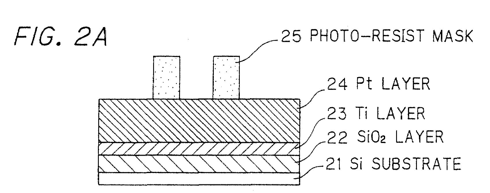
First, a surface of the Si substrate 21 is oxidized by
heating, and thereby a SiO2 layer 22 having a thickness of 200
nm is formed on the surface of the Si substrate 21. Moreover,
a Ti layer 23 having a thickness of 20 nm, and a Pt layer 24
having a thickness of 200 nm are successively formed on the SiO2
layer 22 by spattering. Then, after a photo-resist to be formed
into an etching mask is applied to the Pt layer 24, and a
photo-resist mask 25 is formed as shown in FIG.2A by exposing
and developing the photo-resist by means of a photo-lithography
apparatus.
-
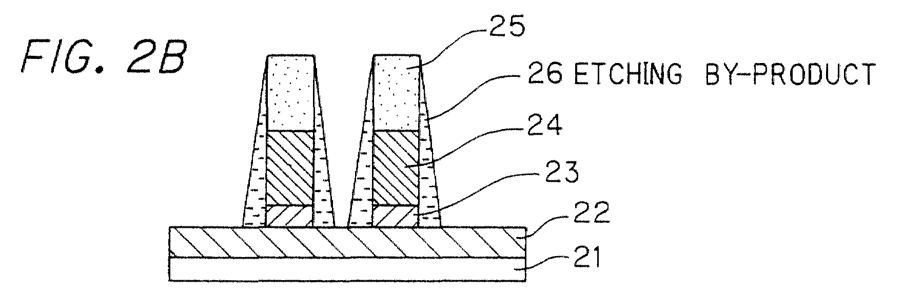
Next, the precious metal layers composed of the Pt layer
24 and the Ti layer 23 are dry etched continuously. The
aforementioned etching process is conducted in accordance with
following conditions. A mixture of Cl2 and Ar is used as an
etching gas. The amount of Cl2 flow rate is 5 SCCM, and the
same of Ar is 145 SCCM. The pressure of the etching gas is kept
to be 5 m TORR, high frequency power of the plasma source is
1300 W, and high frequency power supplied to the bias electrode
14 is 350 W. The temperature of the Si substrate 21 is kept
to be 20 °C. According to the aforementioned conditions, the
etch rate of the Pt layer 24 of 250 nm/min can be obtained. As
shown in FIG.2B, the etching by-products 26 formed of Pt and
PtCl2 are deposited on the both sides of the photo-resist mask
25 as residues like fences.
-
Next, in order to remove the photo-resist mask 25 which
has become unnecessary, the Si substrate 21 is carried to a
reaction chamber (not shown) in which the photo-resist mask 25
is ashed via vacuum transportation chamber(not shown) . In the
reaction chamber, the photo-resist mask 25 is ashed and stripped
by oxygen plasma. In the ashing process, the amount of Cl2 flow
rate is 2000 SCCM, pressure is 3 TORR, and the temperature of
the Si substrate 21 is 200°C. As a result, although the
photo-resist mask 25 is ashed at the ashing rate of 3 nm/min,
the etching by-products 26 are not removed, and remain on the
SiO2 layer 22 as shown in FIG.2C.
-
Next, the Si substrate 21 on which the etching by-products
26 remain is soaked in a mixing solution composed of hfac,
ammonia and DI water serving as a solvent. In the aforementioned
process, the temperature of the mixing solution is room
temperature to 80°C. As a result, the etching by-product 26
reacts with hfac, and is changed into Pt(hfac)2 and dissolved.
In this way, the etching by-product 26 is removed perfectly as
shown in FIG. 2D.
-
Herein, the principle of the phenomenon that the etching
by-product 26 is removed by the wet process will be explained.
-
When PtCl2 or Ircl4 is soaked in the mixing solution
composed of either of hfac or acac, DI water and ammonia,
chemical reactions represented by following chemical equations
take place.
-
When PtCl2 is soaked in the mixing solution composed of
hfac, DI water and ammonia (NH3), PtCl2 is dissolved in
accordance with the following chemical equation.
PtCl2+2H(hfac)+2NH3 = Pt(hfac)2+2NH4Cl
-
Moreover, when IrCl4 is soaked in a mixing solution
composed of hfac, DI water and ammonia, IrCl4 is dissolved in
accordance with the following chemical equaion.
IrCl4+3H(hfac)+3NH3 = Ir(hfac)3+3NH4Cl+(1/2)Cl2
-
Although explanations are given to hfac in the above
descriptions, a similar reaction takes place in case that acac
is used instead of hfac.
-
As mentioned in the above, the etching by-product 26 which
is formed of PtCl2 or IrCl4 and remains on the substrate as
residue like a fence after the photo-resist is ashed can be
easily dissolved by soaking it in the mixing solution composed
of either of hfac or acac and NH3. The invention can be applied
to a case that the Pt layer is dry etched by the other halogenos
gas such as Br2 and F2. The etching by-products formed of Ir
or IrO2 can be also removed by the same method.
-
Although the dry etching process using cl2 gas has been
exemplified in the above explanations, the invention can be also
applied to the dry etching process using Br2, HCl, HBr, SF6 or
F2.
[The second preferred embodiment]
-
Next, the second preferred embodiment of the invention
will be explained. In the second preferred embodiment, since
a process that the photo-resist which has become unnecessary,
after the Pt layer is etched, is ashed is the same as that in
the first preferred embodiment, duplicated explanations will
be omitted.
-
In this embodiment, in order to remove the etching
by-products 26 formed of Pt and PtCl2, the etching by-products
26 are soaked in a mixing solution composed of acac, ammonia
and DI water serving as a solvent. In the aforementioned
process, the temperature of the mixing solution is room
temperature to 80°C. As a result, the etching by-products 26
react with acac and, is changed into Pt(acac)2 having high
saturated vapor pressure and dissolved, so that the etching
by-products 26 which remain on the substrate as residues like
fences are removed perfectly.
[Third Preferred Embodiment]
-
Next, the third preferred embodiment will be explained.
In this embodiment, HBr gas is used as a dry etching gas in stead
of Cl2 gas. The amount of HBr flow rate is 45 SCCM, and the
same of Ar gas is 155 SCCM. The pressure of the etching gas
is fixed to 5 m TORR, high frequency power of the plasma source
is 1100W, and the same supplied to a bias electrode is 350W.
The temperature of the Si substrate 21 is kept to be 20°C. Under
the aforementioned conditions, etch rate of the Pt layer 24 is
320 nm/min.
-
Next, in order to remove the photo-resist mask which has
become unnecessary, the photo-resist mask is ashed by the same
process and under the same conditions as those of the
aforementioned embodiments, and the etching by-products 26
remain on the substrate 21 as residues like fences. Next, the
Si substrate 21 on which the etching by-products 26 are
deposited is soaked in the mixing solution composed of hfac,
NH3 and DI water serving as a solvent. In this case, the
temperature of the mixing solution is room temperature to 80°C.
As a result, the etching by-products 26 react with hfac, and
is changed into Pt(hfac)2 and dissolved, so that the etching
by-products 26 are removed perfectly.
[The Fourth Preferred Embodiment]
-
Next, the fourth preferred embodiment of the invention
will be explained. Since the process that the photo-resist
which has become unnecessary, after the Pt layer is dry etched,
is ashed in the fourth preferred embodiment is the same as those
in the aforementioned embodiments, duplicated explanations
will be omitted. In order to remove the etching by-products
26 which are formed of Pt and PtBr2 and remain on the substrate
21 as residues like fences, the Si substrate 21 on which the
etching by-products 26 remain is soaked in the mixing solution
composed of acac, ammonia and DI water serving as a solvent.
In this case, the temperature of the mixing solution is room
temperature to 80°C. As a result, the etching by-products 26
react with acac, ad change into Pt(acac)2 having the high
saturated vapor pressure, and is dissolved, so that the etching
by-products 26 are removed perfectly.
-
Although the method for removing the etching by-products
formed of Pt and a halogenide of Pt after the Pt layer 24 is
dry etched by a halogenous gas has been explained in the above
descriptions, the etching by-products can be removed by the
aforementioned method in case that Ir or IrO2 is dry etched.
-
As mentioned in the above, according to the method for
fabricating the semiconductor device according to the invention,
since the etching by-products deposited on the side walls of
the electrode can be dissolved in case that a precious metal
layer is dry etched, the etching by-products can be effectively
removed from the side walls of the electrode without dispersion
of particles. As a result, the yield rate of the semiconductor
device is improved, and the productivity of the fabricated goods
can be heightened.