EP1164630A2 - Graded/stepped silicide process to improve MOS transistor - Google Patents
Graded/stepped silicide process to improve MOS transistor Download PDFInfo
- Publication number
- EP1164630A2 EP1164630A2 EP01304400A EP01304400A EP1164630A2 EP 1164630 A2 EP1164630 A2 EP 1164630A2 EP 01304400 A EP01304400 A EP 01304400A EP 01304400 A EP01304400 A EP 01304400A EP 1164630 A2 EP1164630 A2 EP 1164630A2
- Authority
- EP
- European Patent Office
- Prior art keywords
- silicide
- silicon
- forming
- region
- silicide region
- Prior art date
- Legal status (The legal status is an assumption and is not a legal conclusion. Google has not performed a legal analysis and makes no representation as to the accuracy of the status listed.)
- Granted
Links
Images

Classifications
-
- H—ELECTRICITY
- H10—SEMICONDUCTOR DEVICES; ELECTRIC SOLID-STATE DEVICES NOT OTHERWISE PROVIDED FOR
- H10D—INORGANIC ELECTRIC SEMICONDUCTOR DEVICES
- H10D64/00—Electrodes of devices having potential barriers
- H10D64/01—Manufacture or treatment
- H10D64/013—Manufacture or treatment of electrodes having a conductor capacitively coupled to a semiconductor by an insulator
- H10D64/01302—Manufacture or treatment of electrodes having a conductor capacitively coupled to a semiconductor by an insulator the insulator being formed after the semiconductor body, the semiconductor being silicon
- H10D64/01304—Manufacture or treatment of electrodes having a conductor capacitively coupled to a semiconductor by an insulator the insulator being formed after the semiconductor body, the semiconductor being silicon characterised by the conductor
- H10D64/01306—Manufacture or treatment of electrodes having a conductor capacitively coupled to a semiconductor by an insulator the insulator being formed after the semiconductor body, the semiconductor being silicon characterised by the conductor the conductor comprising a layer of silicon contacting the insulator, e.g. polysilicon
- H10D64/01308—Manufacture or treatment of electrodes having a conductor capacitively coupled to a semiconductor by an insulator the insulator being formed after the semiconductor body, the semiconductor being silicon characterised by the conductor the conductor comprising a layer of silicon contacting the insulator, e.g. polysilicon the conductor further comprising a non-elemental silicon additional conductive layer, e.g. a metal silicide layer formed by the reaction of silicon with an implanted metal
- H10D64/01312—Manufacture or treatment of electrodes having a conductor capacitively coupled to a semiconductor by an insulator the insulator being formed after the semiconductor body, the semiconductor being silicon characterised by the conductor the conductor comprising a layer of silicon contacting the insulator, e.g. polysilicon the conductor further comprising a non-elemental silicon additional conductive layer, e.g. a metal silicide layer formed by the reaction of silicon with an implanted metal the additional layer comprising a metal or metal silicide formed by deposition, i.e. without a silicidation reaction, e.g. sputter deposition
-
- H—ELECTRICITY
- H10—SEMICONDUCTOR DEVICES; ELECTRIC SOLID-STATE DEVICES NOT OTHERWISE PROVIDED FOR
- H10D—INORGANIC ELECTRIC SEMICONDUCTOR DEVICES
- H10D64/00—Electrodes of devices having potential barriers
- H10D64/60—Electrodes characterised by their materials
- H10D64/66—Electrodes having a conductor capacitively coupled to a semiconductor by an insulator, e.g. MIS electrodes
- H10D64/661—Electrodes having a conductor capacitively coupled to a semiconductor by an insulator, e.g. MIS electrodes the conductor comprising a layer of silicon contacting the insulator, e.g. polysilicon having vertical doping variation
- H10D64/662—Electrodes having a conductor capacitively coupled to a semiconductor by an insulator, e.g. MIS electrodes the conductor comprising a layer of silicon contacting the insulator, e.g. polysilicon having vertical doping variation the conductor further comprising additional layers, e.g. multiple silicon layers having different crystal structures
- H10D64/663—Electrodes having a conductor capacitively coupled to a semiconductor by an insulator, e.g. MIS electrodes the conductor comprising a layer of silicon contacting the insulator, e.g. polysilicon having vertical doping variation the conductor further comprising additional layers, e.g. multiple silicon layers having different crystal structures the additional layers comprising a silicide layer contacting the layer of silicon, e.g. polycide gates
Definitions
- the present invention relates generally to forming conductive structures within an integrated circuit device, and in particular to forming silicides on conductive structures within an integrated circuit device. Still more particularly, the present invention relates to forming silicides of variable metal concentration as a portion of an integrated circuit device.
- Polysilicon layers are frequently utilized for transistor gates, interconnects, and other conductive structures within integrated circuits.
- doped polysilicon is often employed in those applications. While this reduces the resistance of the conductive structure, the sheet resistance remains higher than desired, e.g., between 20 and 40 Ohms/square ( ⁇ / ⁇ ).
- the doped polysilicon interconnect may introduce a significant transmission delay.
- One method to improve the sheet resistance of doped polysilicon in gate applications that does not require additional masking steps is to combine the polysilicon with a refractory metal.
- Refractory metal silicide films such as tungsten silicide and titanium silicide are formed on the polysilicon conductive structures (with the resulting silicide often being referred to as a "polycide") in integrated circuits, particularly transistor gates. This process results in an improved sheet resistance, on the order of 1 to 5 Ohms/square.
- the use of a silicide gate reduces interconnect resistance and allows the gate to be used as a moderate long-distance interconnect.
- Silicide is also increasingly employed in semiconductor fabrication to reduce the contact resistance to both the gate and the source/drain conductors.
- Silicide formation between a silicon and a refractory metal can be accomplished by several means. Silicides may be formed by depositing a refractory metal layer on an existing polysilicon layer, then annealing the two layers at a sufficiently high temperature to form a silicide at the interface. Alternatively, silicides may be deposited through sputter deposition from a refractory metal silicide target or by chemical vapor deposition utilizing gaseous reactants including both the refractory metal and silicon.
- a silicide with a uniform metal concentration or stochimetric ratio that is, the ratio x/y in Si x R y for a silicide formed with refractory metal R
- a silicide with a uniform metal concentration or stochimetric ratio that is, the ratio x/y in Si x R y for a silicide formed with refractory metal R
- post silicide thermal cycles such as poly oxidation, annealing steps, and the like
- severe problems are known to occur.
- the Si/W ratio is low in tungsten silicide, delamination of the silicide from the underlying structure and tungsten oxidation may occur.
- silicon-rich silicides are commonly employed, but result in high resistivities, require large film thickness, provide poor step coverage, and degrade production throughput in both etch and deposition steps.
- transistor performance, and overall circuit performance may be limited.
- a silicide having variable internal metal concentration tuned to surface conditions at the interface between the silicide and adjoining layers is employed within an integrated circuit. Higher silicon/metal (silicon-rich) ratios are employed near the interfaces to adjoining layers to reduce lattice mismatch with underlying polysilicon or overlying oxide, thereby reducing stress and the likelihood of delamination. A lower silicon/metal ratio is employed within an internal region of the silicide, reducing resistivity. The variable silicon/metal ratio is achieved by controlling reactant gas concentrations or flow rates during deposition of the silicide. Thinner silicides with less likelihood of delamination or metal oxidation may thus be formed.
- FIG. 1 a cross-section of an integrated circuit structure including a silicide formed in accordance with a preferred embodiment of the present invention is depicted.
- the process begins with an integrated circuit structure including a substrate 100 on which is formed an isolation oxide 102 having an opening 104 therethrough defining an active region.
- a transistor gate structure including a gate oxide 106 and a polysilicon gate electrode 108 .
- a silicide 110 is formed on the gate electrode 108 .
- Sidewall spacers 112 are formed adjacent the gate structure, and source/drain regions 114 are formed within the substrate 100 adjacent the gate structure and partially underlying sidewalls spacers 112 .
- silicide 110 may be formed utilizing known processing techniques. To resolve the problems described above, a silicide process with a graded or stepped silicon/refractory metal ratio is employed. Silicide 110 is formed with a variable internal composition in which the ratio of silicon to refractory metal is different at the interfaces between silicide 110 and polysilicon 108 and between silicide 110 and an overlying oxide differs from the ratio of silicon to the refractory metal within a central region.
- the silicide 110 should have both low sheet resistance and thin thickness.
- silicide delamination during subsequent thermal cycles is more prevalent among thinner silicide films, and is mainly caused by the presence of interface defects between the underlying polysilicon and the silicide (clean process), and by silicide film stress, typically resulting from lattice mismatch between the silicide and the adjoining layers. Therefore formation of a thin silicide with low sheet resistance is difficult to achieve since increasing refractory metal concentration to reduce resistivity increases stress.
- Silicide 110 includes different metal concentrations, or silicon/refractory metal ratios, within different regions.
- a first region 110a near the interface between silicide 110 and the polysilicon gate electrode 108 is silicon-rich, as is a second region 110b near the opposite surface of the silicide layer 110 .
- a central region 110c is less silicon-rich, providing a lower resistivity for the overall structure. The silicon-rich regions near the silicide interfaces reduce the likelihood of delamination, which typically results from lattice mismatch between adjoining layers.
- the first and second regions 110a-110b which preferably have a thickness of less than about 200 ⁇ , may have an Si/W ratio of about 3.3.
- the central region 110c which preferably has a thickness of about 900 ⁇ , may have an Si/W ratio of about 2.2.
- the silicon-rich layers near the interfaces improve lattice mismatch between the silicide 110 and the underlying polysilicon and between the silicide 110 and an overlying oxide (not shown).
- the central region provides a reduced resistivity for the overall structure, which is all at the same electrical potential such that the electrical properties are not significantly affected by the silicon-rich regions near the interfaces.
- a plot of resistivity for tungsten silicide layers as a function of the silicon/tungsten (Si/W) ratio x is depicted in Figure 3 .
- the ratio of silicon to refractory metal may be controlled by controlling the flow rates of the reactant gases.
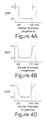
- the internal composition of a silicide layer may include step changes in silicon/tungsten ratio a illustrated in Figure 4A (i.e., formed by distinct layers), gradual changes as illustrated in Figure 4B , or continuous changes as illustrated in Figure 4C .
- the present invention may be employed with any metal silicide, including titanium silicide, tantalum silicide, or cobalt silicide.
- metal silicide including titanium silicide, tantalum silicide, or cobalt silicide.
- the particular stochiometric ratios of silicon to refractory metal within regions 110a and 110b of silicide 110 are preferably tuned to the particular process employed and to the surface conditions of the adjoining layers. Silicide regions 110a and 110b thus act as "glue" layers promoting adhesion between layers, and allowing a thinner silicide 110 to be employed, consistent with smaller device feature sizes.
- the present invention allows a reduction of silicide sheet resistivity to increase device performance while also reducing silicide thickness to improve topological step coverage. Thinner silicides improve productivity due to reduced thickness and increase deposition rates, and also reduces the risk of delamination. The poly depletion effect is reduced as a result of lower gate resistivity, and the risk of gate oxide degradation due to flourine penetration is also reduced. Metal oxidation on top of the silicide may be avoided due to the silicon-rich character to the upper surface region.
Landscapes
- Electrodes Of Semiconductors (AREA)
- Internal Circuitry In Semiconductor Integrated Circuit Devices (AREA)
- Insulated Gate Type Field-Effect Transistor (AREA)
Abstract
Description
Claims (14)
- A method of forming a portion of an integrated circuit, comprising:forming a first silicide region over a device structure within the integrated circuit, the first silicide region having a first silicon/metal ratio; andforming a second silicide region on the first silicide region, the second silicide region having a second silicon/metal ratio greater than the first silicon/metal ratio.
- The method of claim 1, further comprising:
forming a third silicide region between the device structure and the first silicide region, the third silicide region having a third silicon/metal ratio greater than the first silicon/metal ratio. - The method of claim 2, wherein the steps of forming a first silicide region, forming a second silicide region, and forming a third silicide region further comprise:
forming a silicide layer having stepped changes in silicon/metal ratio across a thickness of the silicide layer. - The method of claim 2, wherein the steps of forming a first silicide region, forming a second silicide region, and forming a third silicide region further comprise:
forming a silicide layer having gradual changes in silicon/metal ratio across a thickness of the silicide layer. - The method of claim 2, wherein the steps of forming a first silicide region, forming a second silicide region, and forming a third silicide region further comprise:
forming a silicide layer having continuous changes in silicon/metal ratio across a thickness of the silicide layer. - The method of claim 2, further comprising:forming the first silicide region with a silicon/metal ratio of 2.2; andforming the second and third silicide regions with a silicon/metal ration of 3.3.
- A portion of an integrated circuit, comprising:wherein the silicide has higher stochiometric ratios of silicon to metal at interfaces between the silicide and the polysilicon conductive structure and between the silicide and the oxide than within an inner region of the silicide.a polysilicon conductive structure;a silicide on the polysilicon conductive structure; andan oxide on the silicide,
- A method of forming a portion of an integrated circuit, comprising:wherein the silicide has higher stochiometric ratios of silicon to metal at interfaces between the silicide and the polysilicon conductive structure and between the silicide and the oxide than within an inner region of the silicide.forming a polysilicon conductive structure;forming a silicide on the polysilicon conductive structure; andforming an oxide on the silicide,
- A portion of an integrated circuit, comprising:a first silicide region over a device structure within the integrated circuit, the first silicide region having a first silicon/metal ratio; anda second silicide region on the first silicide region, the second silicide region having a second silicon/metal ratio greater than the first silicon/metal ratio.
- The portion of an integrated circuit of claim 9, further comprising:
a third silicide region between the device structure and the first silicide region, the third silicide region having a third silicon/metal ratio greater than the first silicon/metal ratio. - The portion of an integrated circuit of claim 10, wherein the first silicide region, the second silicide region, and the third silicide region further comprise:
a silicide layer having stepped changes in silicon/metal ratio across a thickness of the silicide layer. - The portion of an integrated circuit of claim 10, wherein the first silicide region, the second silicide region, and the third silicide region further comprise:
a silicide layer having gradual changes in silicon/metal ratio across a thickness of the silicide layer. - The portion of an integrated circuit of claim 10, wherein the first silicide region, the second silicide region, and the third silicide region further comprise:
a silicide layer having continuous changes in silicon/metal ratio across a thickness of the silicide layer. - The portion of an integrated circuit of claim 10, further comprising:the first silicide region with a silicon/metal ratio of 2.2; andthe second and third silicide regions with a silicon/metal ration of 3.3.
Applications Claiming Priority (2)
| Application Number | Priority Date | Filing Date | Title |
|---|---|---|---|
| US09/594,868 US6350684B1 (en) | 2000-06-15 | 2000-06-15 | Graded/stepped silicide process to improve MOS transistor |
| US594868 | 2000-06-15 |
Publications (3)
| Publication Number | Publication Date |
|---|---|
| EP1164630A2 true EP1164630A2 (en) | 2001-12-19 |
| EP1164630A3 EP1164630A3 (en) | 2002-12-18 |
| EP1164630B1 EP1164630B1 (en) | 2006-07-05 |
Family
ID=24380751
Family Applications (1)
| Application Number | Title | Priority Date | Filing Date |
|---|---|---|---|
| EP01304400A Expired - Lifetime EP1164630B1 (en) | 2000-06-15 | 2001-05-18 | Silicide process having a variable silicon/metal ratio |
Country Status (4)
| Country | Link |
|---|---|
| US (2) | US6350684B1 (en) |
| EP (1) | EP1164630B1 (en) |
| JP (1) | JP2002033294A (en) |
| DE (1) | DE60121258D1 (en) |
Families Citing this family (5)
| Publication number | Priority date | Publication date | Assignee | Title |
|---|---|---|---|---|
| WO2003019643A1 (en) * | 2001-08-23 | 2003-03-06 | Nec Corporation | Semiconductor device having high-permittivity insulation film and production method therefor |
| CN1989597A (en) * | 2004-07-30 | 2007-06-27 | 应用材料股份有限公司 | Thin tungsten silicide layer deposition and gate metal integration |
| KR100650858B1 (en) * | 2005-12-23 | 2006-11-28 | 주식회사 하이닉스반도체 | Manufacturing Method of Flash Memory Device |
| US8741773B2 (en) * | 2010-01-08 | 2014-06-03 | International Business Machines Corporation | Nickel-silicide formation with differential Pt composition |
| US10903330B2 (en) * | 2013-11-27 | 2021-01-26 | General Electric Company | Tapered gate electrode for semiconductor devices |
Family Cites Families (11)
| Publication number | Priority date | Publication date | Assignee | Title |
|---|---|---|---|---|
| US4954852A (en) * | 1987-12-24 | 1990-09-04 | Ford Microelectronics, Inc. | Sputtered metallic silicide gate for GaAs integrated circuits |
| EP0785574A3 (en) * | 1996-01-16 | 1998-07-29 | Applied Materials, Inc. | Method of forming tungsten-silicide |
| US5654219A (en) * | 1996-02-07 | 1997-08-05 | Texas Instruments Incorporated | Annealed poly-silicide etch process |
| US5635765A (en) | 1996-02-26 | 1997-06-03 | Cypress Semiconductor Corporation | Multi-layer gate structure |
| US5725739A (en) * | 1996-07-08 | 1998-03-10 | Micron Technology, Inc. | Low angle, low energy physical vapor deposition of alloys |
| US6087254A (en) * | 1996-07-16 | 2000-07-11 | Micron Technology, Inc. | Technique for elimination of pitting on silicon substrate during gate stack etch |
| US6153452A (en) * | 1997-01-07 | 2000-11-28 | Lucent Technologies Inc. | Method of manufacturing semiconductor devices having improved polycide integrity through introduction of a silicon layer within the polycide structure |
| KR100243291B1 (en) * | 1997-04-30 | 2000-03-02 | 윤종용 | Method for forming silicide layers in processes fabricating a semiconductor device |
| JPH11200050A (en) * | 1998-01-14 | 1999-07-27 | Mitsubishi Electric Corp | Method for forming tungsten silicide film, method for manufacturing semiconductor device, and semiconductor wafer processing apparatus |
| US6103607A (en) * | 1998-09-15 | 2000-08-15 | Lucent Technologies | Manufacture of MOSFET devices |
| US6331460B1 (en) * | 1999-11-17 | 2001-12-18 | Agere Systems Guardian Corp. | Method of fabricating a mom capacitor having a metal silicide barrier |
-
2000
- 2000-06-15 US US09/594,868 patent/US6350684B1/en not_active Expired - Lifetime
-
2001
- 2001-05-18 DE DE60121258T patent/DE60121258D1/en not_active Expired - Lifetime
- 2001-05-18 EP EP01304400A patent/EP1164630B1/en not_active Expired - Lifetime
- 2001-06-13 JP JP2001179122A patent/JP2002033294A/en active Pending
-
2003
- 2003-04-28 US US10/424,800 patent/US7465660B2/en not_active Expired - Fee Related
Also Published As
| Publication number | Publication date |
|---|---|
| EP1164630A3 (en) | 2002-12-18 |
| US7465660B2 (en) | 2008-12-16 |
| EP1164630B1 (en) | 2006-07-05 |
| US6350684B1 (en) | 2002-02-26 |
| DE60121258D1 (en) | 2006-08-17 |
| JP2002033294A (en) | 2002-01-31 |
| US20030211733A1 (en) | 2003-11-13 |
Similar Documents
| Publication | Publication Date | Title |
|---|---|---|
| US5907784A (en) | Method of making multi-layer gate structure with different stoichiometry silicide layers | |
| KR100204083B1 (en) | Tasin oxygen diffusion barrier in multilayer structure | |
| US5365111A (en) | Stable local interconnect/active area silicide structure for VLSI applications | |
| US5877074A (en) | Method for improving the electrical property of gate in polycide structure | |
| US20030139061A1 (en) | Barrier in gate stack for improved gate dielectric integrity | |
| CN1167336A (en) | Manufacturing method of multilayer amorphous silicon | |
| US6908849B2 (en) | High aspect ratio contact structure with reduced silicon consumption | |
| US6461960B2 (en) | Method of manufacturing a semiconductor device | |
| JPS61501358A (en) | Improved integrated circuit structure with intermediate metal silicide layer and method of fabrication thereof | |
| US7875939B2 (en) | Semiconductor device including an ohmic layer | |
| US6635938B1 (en) | Semiconductor device and manufacturing method thereof | |
| US7465660B2 (en) | Graded/stepped silicide process to improve MOS transistor | |
| US6586320B2 (en) | Graded/stepped silicide process to improve mos transistor | |
| US6245620B1 (en) | Method for foaming MOS transistor having bi-layered spacer | |
| JPH08116057A (en) | Method for manufacturing TiN gate electrode of semiconductor device | |
| US6627504B1 (en) | Stacked double sidewall spacer oxide over nitride | |
| KR20020016312A (en) | The method of fabricating tungsten-gate | |
| US5946599A (en) | Method of manufacturing a semiconductor IC device | |
| KR100210853B1 (en) | Conducting line of semiconductor device and method of manufacturing the same | |
| JP2000049340A (en) | Semiconductor device and fabrication thereof | |
| US6555887B1 (en) | Semiconductor device with multi-layer interconnection | |
| US6127270A (en) | Methods of forming refractory metal silicide components and methods of restricting silicon surface migration of a silicon structure | |
| KR100364524B1 (en) | Method for Forming MOS Transistor Having Single-Layer Gate Structure Made of Tungsten Silicide | |
| KR100400279B1 (en) | Method of manufacturing a semiconductor device having tungsten silicide | |
| JPS61156885A (en) | Polycrystalline semiconductor device and manufacture thereof |
Legal Events
| Date | Code | Title | Description |
|---|---|---|---|
| PUAI | Public reference made under article 153(3) epc to a published international application that has entered the european phase |
Free format text: ORIGINAL CODE: 0009012 |
|
| AK | Designated contracting states |
Kind code of ref document: A2 Designated state(s): AT BE CH CY DE DK ES FI FR GB GR IE IT LI LU MC NL PT SE TR |
|
| AX | Request for extension of the european patent |
Free format text: AL;LT;LV;MK;RO;SI |
|
| PUAL | Search report despatched |
Free format text: ORIGINAL CODE: 0009013 |
|
| RIC1 | Information provided on ipc code assigned before grant |
Free format text: 7H 01L 21/28 A, 7H 01L 29/49 B |
|
| AK | Designated contracting states |
Kind code of ref document: A3 Designated state(s): AT BE CH CY DE DK ES FI FR GB GR IE IT LI LU MC NL PT SE TR |
|
| AX | Request for extension of the european patent |
Free format text: AL;LT;LV;MK;RO;SI |
|
| 17P | Request for examination filed |
Effective date: 20030605 |
|
| AKX | Designation fees paid |
Designated state(s): DE FR GB IT |
|
| 17Q | First examination report despatched |
Effective date: 20030813 |
|
| GRAP | Despatch of communication of intention to grant a patent |
Free format text: ORIGINAL CODE: EPIDOSNIGR1 |
|
| GRAC | Information related to communication of intention to grant a patent modified |
Free format text: ORIGINAL CODE: EPIDOSCIGR1 |
|
| RTI1 | Title (correction) |
Free format text: SILICIDE PROCESS HAVING A VARIABLE SILICON/METAL RATIO |
|
| GRAS | Grant fee paid |
Free format text: ORIGINAL CODE: EPIDOSNIGR3 |
|
| GRAA | (expected) grant |
Free format text: ORIGINAL CODE: 0009210 |
|
| AK | Designated contracting states |
Kind code of ref document: B1 Designated state(s): DE FR GB IT |
|
| PG25 | Lapsed in a contracting state [announced via postgrant information from national office to epo] |
Ref country code: IT Free format text: LAPSE BECAUSE OF FAILURE TO SUBMIT A TRANSLATION OF THE DESCRIPTION OR TO PAY THE FEE WITHIN THE PRESCRIBED TIME-LIMIT;WARNING: LAPSES OF ITALIAN PATENTS WITH EFFECTIVE DATE BEFORE 2007 MAY HAVE OCCURRED AT ANY TIME BEFORE 2007. THE CORRECT EFFECTIVE DATE MAY BE DIFFERENT FROM THE ONE RECORDED. Effective date: 20060705 |
|
| REG | Reference to a national code |
Ref country code: GB Ref legal event code: FG4D |
|
| REF | Corresponds to: |
Ref document number: 60121258 Country of ref document: DE Date of ref document: 20060817 Kind code of ref document: P |
|
| PG25 | Lapsed in a contracting state [announced via postgrant information from national office to epo] |
Ref country code: DE Free format text: LAPSE BECAUSE OF FAILURE TO SUBMIT A TRANSLATION OF THE DESCRIPTION OR TO PAY THE FEE WITHIN THE PRESCRIBED TIME-LIMIT Effective date: 20061006 |
|
| ET | Fr: translation filed | ||
| PLBE | No opposition filed within time limit |
Free format text: ORIGINAL CODE: 0009261 |
|
| STAA | Information on the status of an ep patent application or granted ep patent |
Free format text: STATUS: NO OPPOSITION FILED WITHIN TIME LIMIT |
|
| 26N | No opposition filed |
Effective date: 20070410 |
|
| REG | Reference to a national code |
Ref country code: FR Ref legal event code: PLFP Year of fee payment: 16 |
|
| REG | Reference to a national code |
Ref country code: FR Ref legal event code: PLFP Year of fee payment: 17 |
|
| REG | Reference to a national code |
Ref country code: FR Ref legal event code: PLFP Year of fee payment: 18 |
|
| PGFP | Annual fee paid to national office [announced via postgrant information from national office to epo] |
Ref country code: FR Payment date: 20200422 Year of fee payment: 20 |
|
| PGFP | Annual fee paid to national office [announced via postgrant information from national office to epo] |
Ref country code: GB Payment date: 20200423 Year of fee payment: 20 |
|
| REG | Reference to a national code |
Ref country code: GB Ref legal event code: PE20 Expiry date: 20210517 |
|
| PG25 | Lapsed in a contracting state [announced via postgrant information from national office to epo] |
Ref country code: GB Free format text: LAPSE BECAUSE OF EXPIRATION OF PROTECTION Effective date: 20210517 |