EP1160980A2 - Intermediate frequency circuit of digital television tuner having flat transmission characteristic in intermediate frequency band - Google Patents
Intermediate frequency circuit of digital television tuner having flat transmission characteristic in intermediate frequency band Download PDFInfo
- Publication number
- EP1160980A2 EP1160980A2 EP01304511A EP01304511A EP1160980A2 EP 1160980 A2 EP1160980 A2 EP 1160980A2 EP 01304511 A EP01304511 A EP 01304511A EP 01304511 A EP01304511 A EP 01304511A EP 1160980 A2 EP1160980 A2 EP 1160980A2
- Authority
- EP
- European Patent Office
- Prior art keywords
- intermediate frequency
- frequency band
- transistor
- capacitor
- low
- Prior art date
- Legal status (The legal status is an assumption and is not a legal conclusion. Google has not performed a legal analysis and makes no representation as to the accuracy of the status listed.)
- Withdrawn
Links
Images
Classifications
-
- H—ELECTRICITY
- H04—ELECTRIC COMMUNICATION TECHNIQUE
- H04N—PICTORIAL COMMUNICATION, e.g. TELEVISION
- H04N5/00—Details of television systems
- H04N5/44—Receiver circuitry for the reception of television signals according to analogue transmission standards
- H04N5/4446—IF amplifier circuits specially adapted for B&W TV
-
- H—ELECTRICITY
- H03—ELECTRONIC CIRCUITRY
- H03F—AMPLIFIERS
- H03F3/00—Amplifiers with only discharge tubes or only semiconductor devices as amplifying elements
- H03F3/189—High-frequency amplifiers, e.g. radio frequency amplifiers
- H03F3/19—High-frequency amplifiers, e.g. radio frequency amplifiers with semiconductor devices only
- H03F3/191—Tuned amplifiers
-
- H—ELECTRICITY
- H03—ELECTRONIC CIRCUITRY
- H03J—TUNING RESONANT CIRCUITS; SELECTING RESONANT CIRCUITS
- H03J1/00—Details of adjusting, driving, indicating, or mechanical control arrangements for resonant circuits in general
-
- H—ELECTRICITY
- H04—ELECTRIC COMMUNICATION TECHNIQUE
- H04N—PICTORIAL COMMUNICATION, e.g. TELEVISION
- H04N21/00—Selective content distribution, e.g. interactive television or video on demand [VOD]
- H04N21/40—Client devices specifically adapted for the reception of or interaction with content, e.g. set-top-box [STB]; Operations thereof
- H04N21/41—Structure of client; Structure of client peripherals
- H04N21/426—Internal components of the client ; Characteristics thereof
-
- H—ELECTRICITY
- H04—ELECTRIC COMMUNICATION TECHNIQUE
- H04N—PICTORIAL COMMUNICATION, e.g. TELEVISION
- H04N21/00—Selective content distribution, e.g. interactive television or video on demand [VOD]
- H04N21/40—Client devices specifically adapted for the reception of or interaction with content, e.g. set-top-box [STB]; Operations thereof
- H04N21/41—Structure of client; Structure of client peripherals
- H04N21/426—Internal components of the client ; Characteristics thereof
- H04N21/42607—Internal components of the client ; Characteristics thereof for processing the incoming bitstream
- H04N21/4263—Internal components of the client ; Characteristics thereof for processing the incoming bitstream involving specific tuning arrangements, e.g. two tuners
Definitions
- the present invention relates to an intermediate frequency circuit of a digital television tuner and, more particularly, to an intermediate frequency circuit of a digital television tuner capable of outputting an intermediate frequency signal of a digital television with a characteristic which is flat in an intermediate frequency band.
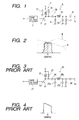
- Fig. 3 shows a conventional intermediate frequency circuit of a digital television tuner (hereinbelow, called intermediate frequency circuit).
- An intermediate frequency signal of a digital television outputted from a not-illustrated mixer passes through an SAW filter 21 for band regulation and is supplied to (the base of) a transistor 22 for amplifying intermediate frequencies.
- a power source voltage is supplied to the collector of the transistor 22 via a choke inductor 23.
- An intermediate frequency signal outputted from the collector is supplied to a low-pass filter 25 via a DC blocking capacitor 24.
- the low-pass filter 25 is connected to an output terminal 26.
- the low-pass filter 25 takes the form of a n type low-pass filter having an input-side shunted capacitor 25a, a serial inductance device 25b, and an output-side shunted capacitor 25c. Its cut-off frequency is higher than the frequencies in the intermediate frequency band.
- a nominal impedance is set so as to be a few hundreds ⁇ (ohm) in relation to a circuit to be connected at the next stage.
- a resistor 27 is connected in parallel to the choke inductor 23.
- a resistor 28 is connected in parallel to the output-side shunted capacitor 25c.
- the transmission characteristic in the output terminal 26 is determined mainly by the transmission characteristic of the SAW filter 21 and the amplification characteristic of the transistor 22.
- the transmission characteristic in the output terminal 26 is as shown in Fig. 4 that the level in the intermediate frequency band (8 MHz) is inclined.
- the level is high at low frequencies and becomes low at high frequencies for the following reason. The higher the frequency becomes, the more the gain of the transistor 22 decreases and, further, the cut-off frequency of the low-pass filter 25 is higher than the intermediate frequency band.
- An object of the invention is, therefore, to provide an intermediate frequency circuit having a flat transmission characteristic in an intermediate frequency band, and in which a transistor is prevented from being destroyed by a shock wave of static electricity or the like applied to the output side.
- an intermediate frequency circuit of a digital television tuner of the invention has: a transistor for amplifying a television signal in an intermediate frequency band; a low-pass filter provided between a collector of the transistor and an output terminal; and a parallel tuning circuit provided between the collector of the transistor and the ground.
- a cut-off frequency of the low-pass filter and a tuning frequency of the parallel tuning circuit is set to be equal to or higher than the intermediate frequency band.
- the parallel tuning circuit and the low-pass filter are coupled to each other via a first capacitor
- the parallel tuning circuit has at least an inductance device for supplying a power source voltage to the collector of the transistor, a terminal on the power source side of the inductance device is connected to the ground via a second capacitor, and a reactance of the first capacitor at a frequency equal to or lower than the intermediate frequency band is set to be larger than a reactance of the second capacitor.
- the reactance of the first capacitor at a frequency in the intermediate frequency band is set to be smaller than a nominal impedance of the low-pass filter.
- Fig. 1 shows an intermediate frequency circuit of a digital television tuner of the invention.
- An intermediate frequency signal of a digital television (simply called an intermediate frequency signal) outputted from a mixer (not shown) passes through an SAW filter 1 for band regulation and is supplied to (the base of) a transistor 2 for amplifying intermediate frequencies.
- a power source voltage is supplied to the collector of the transistor 2 via a choke inductor 3a as an inductance device.
- a capacitor 3b is connected in parallel to the choke inductor 3a, and a parallel tuning circuit 3 is constructed by the choke inductor 3a and the capacitor 3b.
- the tuning frequency of the parallel tuning circuit 3 is set so as to be higher than a frequency band (intermediate frequency band) of the intermediate frequency signal.
- a frequency band intermediate frequency band
- the tuning frequency is set to about 50 to 70 MHz.
- a low-pass filter 5 is connected to the parallel tuning circuit 3 via a first capacitor 4.
- the low-pass filter 5 takes the form of an L-type low-pass filter constructed by a serial inductance device 5a and an output-side shunted capacitor 5b.
- the cut-off frequency is higher than the intermediate frequency band and is set to about 60 to 80 MHz.
- a nominal impedance of the low-pass filter 5 is set so as to be about 300 ⁇ (ohm) in relation with a circuit to be connected at the next stage. Consequently, the input side of the low-pass filter 5 is shunted by a resistor 6 of 600 ⁇ and the output side is also shunted by a resistor 7 of 600 ⁇ . The output side of the low-pass filter 5 is connected to an output terminal 9 via a DC blocking capacitor 8.
- One end on the power source side of the choke inductor 3a for supplying a power source voltage to the collector of the transistor 2 is connected to the ground via a second capacitor 10.
- Each of the reactance of the second capacitor 10 and that of the choke inductor 3a at a frequency lower than the intermediate frequency band is set to be smaller than the reactance of the first capacitor 4. Further, the reactance of the first capacitor 4 is smaller than the nominal impedance of the low-pass filter 5 in the intermediate frequency band.
- the transmission characteristic in the intermediate frequency band at the output terminal 9 is determined mainly by the transmission characteristic of the SAW filter 1, amplification characteristic of the transistor 2, and transmission characteristics of the parallel tuning circuit 3 and the low-pass filter 5.
- the SAW filter 1 has flat characteristics in which a center frequency is about 36 MHz and a passband is 8 MHz. As the frequency becomes higher, the gain of the transistor 2 decreases, so that a declining characteristic is obtained. Since the low-pass filter 5 has a cut-off frequency higher than the intermediate frequency band, a declining characteristic is similarly obtained. The characteristic obtained from both of the characteristics is as shown by a curve A in Fig. 2. On the other hand, since the parallel tuning circuit 3 itself has a tuning frequency higher than the intermediate frequency band, a climbing characteristic as shown by a curve B in Fig. 2 is obtained.
- the transmission characteristic as a whole becomes flat in the intermediate frequency band as shown by a hatched portion in Fig. 2.
- the intermediate frequency signal of a digital television becomes flat in the intermediate frequency band. Since the tuning frequency of the parallel tuning circuit 5 lies out of the intermediate frequency band, a signal is outputted without deteriorating a group delay, and a video image is reproduced with high fidelity.
- the reactance of the second capacitor 10 is smaller than that of the first capacitor 4. Consequently, an external voltage having a frequency component lower than the intermediate frequency band, such as static electricity, a shock wave, and the like entering from the output terminal 9 is attenuated by the first capacitor 4 and is connected to the ground via the choke inductor 3a and the second capacitor 10 so as to bypass the transistor 2.
- the transistor 2 is, therefore, not easily destroyed.
- the capacitor 3b as a component of the parallel tuning circuit 5 can also serve as an input-side shunted capacitor of the low-pass filter 5.
- the intermediate frequency circuit of a digital television tuner of the invention has: the transistor for amplifying a television signal in an intermediate frequency band; the low-pass filter provided between a collector of the transistor and an output terminal; and the parallel tuning circuit provided between the collector of the transistor and the ground.
- Each of a cut-off frequency of the low-pass filter and a tuning frequency of the parallel tuning circuit is set to be equal to or higher than the intermediate frequency band.
- the intermediate frequency signal of the digital television is outputted with the flat characteristic in the intermediate frequency band. Without deteriorating a group delay, a video image can be reproduced with high fidelity.
- the parallel tuning circuit and the low-pass filter are coupled to each other via a first capacitor
- the parallel tuning circuit has at least an inductance device for supplying a power source voltage to the collector of the transistor, a terminal on the power source side of the inductance device is connected to the ground via a second capacitor, and a reactance of the first capacitor at a frequency equal to or lower than the intermediate frequency band is set to be larger than a reactance of the second capacitor. Consequently, an external voltage having a frequency component lower than the intermediate frequency band, such as static electricity, a shock wave, and the like entering from the output terminal is attenuated by the first capacitor and is connected to the ground via the choke inductor and the second capacitor so as to bypass the transistor. The transistor is, therefore, not easily destroyed.
- the reactance of the first capacitor at a frequency in the intermediate frequency band is set to be smaller than a nominal impedance of the low-pass filter. Consequently, the capacitor as a component of the parallel tuning circuit can also serve as an input-side shunted capacitor of the low-pass filter, so that the number of parts in the specification can be reduced.
Landscapes
- Engineering & Computer Science (AREA)
- Multimedia (AREA)
- Signal Processing (AREA)
- Power Engineering (AREA)
- Filters And Equalizers (AREA)
- Superheterodyne Receivers (AREA)
- Amplifiers (AREA)
Abstract
Description
Claims (3)
- An intermediate frequency circuit of a digital television tuner, comprising:a transistor for amplifying a television signal in an intermediate frequency band;a low-pass filter provided between a collector of the transistor and an output terminal; anda parallel tuning circuit provided between the collector of the transistor and a ground,wherein each of a cut-off frequency of the low-pass filter and a tuning frequency of the parallel tuning circuit is set to be equal to or higher than the intermediate frequency band.
- An intermediate frequency circuit of a digital television tuner according to claim 1, wherein the parallel tuning circuit and the low-pass filter are coupled to each other via a first capacitor, the parallel tuning circuit has at least an inductance device for supplying a power source voltage to the collector of the transistor, a terminal on the power source side of the inductance device is connected to the ground via a second capacitor, and a reactance of the first capacitor at a frequency equal to or lower than the intermediate frequency band is set to be larger than a reactance of the second capacitor.
- An intermediate frequency circuit of a digital television tuner according to claim 2, wherein the reactance of the first capacitor at a frequency in the intermediate frequency band is set to be smaller than a nominal impedance of the low-pass filter.
Applications Claiming Priority (2)
| Application Number | Priority Date | Filing Date | Title |
|---|---|---|---|
| JP2000166463 | 2000-05-31 | ||
| JP2000166463A JP2001346111A (en) | 2000-05-31 | 2000-05-31 | Intermediate frequency circuit for digital television tuner |
Publications (2)
| Publication Number | Publication Date |
|---|---|
| EP1160980A2 true EP1160980A2 (en) | 2001-12-05 |
| EP1160980A3 EP1160980A3 (en) | 2004-01-02 |
Family
ID=18669779
Family Applications (1)
| Application Number | Title | Priority Date | Filing Date |
|---|---|---|---|
| EP01304511A Withdrawn EP1160980A3 (en) | 2000-05-31 | 2001-05-23 | Intermediate frequency circuit of digital television tuner having flat transmission characteristic in intermediate frequency band |
Country Status (3)
| Country | Link |
|---|---|
| US (1) | US6678013B2 (en) |
| EP (1) | EP1160980A3 (en) |
| JP (1) | JP2001346111A (en) |
Families Citing this family (2)
| Publication number | Priority date | Publication date | Assignee | Title |
|---|---|---|---|---|
| JP2004048121A (en) * | 2002-07-09 | 2004-02-12 | Alps Electric Co Ltd | Television tuner |
| JP3099083U (en) * | 2003-07-07 | 2004-03-25 | アルプス電気株式会社 | Television tuner |
Family Cites Families (9)
| Publication number | Priority date | Publication date | Assignee | Title |
|---|---|---|---|---|
| JPS5527759A (en) * | 1978-08-21 | 1980-02-28 | Hitachi Ltd | Monolithic semiconductor integrated circuit for television |
| JPS57157607A (en) * | 1981-03-24 | 1982-09-29 | Toshiba Corp | Hybrid integrated circuit |
| US4994761A (en) * | 1989-11-06 | 1991-02-19 | Motorola Inc. | VHF power amplifier |
| DE3939740C2 (en) * | 1989-12-01 | 1996-11-28 | Telefunken Microelectron | Mixing stage |
| FR2673054B1 (en) * | 1991-02-18 | 1996-12-13 | Matra Communication | HIGH STABILITY AMPLIFIER. |
| JPH05206738A (en) | 1992-01-24 | 1993-08-13 | Sharp Corp | FET mixer |
| JPH08167012A (en) * | 1994-12-13 | 1996-06-25 | Toshiba Corp | Data storage medium |
| US5737035A (en) * | 1995-04-21 | 1998-04-07 | Microtune, Inc. | Highly integrated television tuner on a single microcircuit |
| JP3961102B2 (en) | 1998-02-20 | 2007-08-22 | 株式会社日立国際電気 | Amplitude equalizer for mobile phone relay amplifier |
-
2000
- 2000-05-31 JP JP2000166463A patent/JP2001346111A/en not_active Withdrawn
-
2001
- 2001-05-23 EP EP01304511A patent/EP1160980A3/en not_active Withdrawn
- 2001-05-29 US US09/867,917 patent/US6678013B2/en not_active Expired - Fee Related
Also Published As
| Publication number | Publication date |
|---|---|
| US6678013B2 (en) | 2004-01-13 |
| JP2001346111A (en) | 2001-12-14 |
| US20010048488A1 (en) | 2001-12-06 |
| EP1160980A3 (en) | 2004-01-02 |
Similar Documents
| Publication | Publication Date | Title |
|---|---|---|
| JPH0614501Y2 (en) | Band-pass filter in converter for CATV | |
| CN1069477C (en) | Parallel untuned video if amplifiers supplied signals from TV 1st detector via respective input filters | |
| US4764736A (en) | Amplifier for high frequency signal | |
| JP3442208B2 (en) | High frequency electronic circuit | |
| KR100466077B1 (en) | Radio frequency modulator having c/l delay compensation function, and set-top-box using that | |
| US6566953B2 (en) | High-frequency amplifier circuit for UHF television tuner having less distortion | |
| US6678013B2 (en) | Intermediate frequency circuit of digital television tuner having flat transmission characteristic in intermediate frequency band | |
| US5276403A (en) | Nonlinear preemphasis-deemphasis system | |
| US6583826B1 (en) | Intermediate frequency circuit in television tuner with large attenuation of audio if signal in adjacent channel | |
| US4611179A (en) | Wide-band type high-frequency amplifier circuit | |
| JP2003229791A (en) | Equalizer | |
| JP2509493B2 (en) | Preamplifier for television receiver | |
| JP2001196961A (en) | Intermediate frequency input circuit | |
| JP2003197433A (en) | Transmission line transformer and amplification unit using the same | |
| JPH06284090A (en) | Optical receiver | |
| JP2002232241A (en) | Pre-distortion circuit | |
| KR200145204Y1 (en) | Audio signal trap circuit | |
| JP2998107B2 (en) | Intermediate frequency amplifier | |
| JPS646602Y2 (en) | ||
| JPH051132Y2 (en) | ||
| JP3145690B2 (en) | Gyrator delay circuit | |
| CN1194536A (en) | Video frequency signal replay circuit | |
| JPH10336543A (en) | Video output circuit | |
| JP2003348469A (en) | Television tuner | |
| JP2007158660A (en) | High-frequency circuit |
Legal Events
| Date | Code | Title | Description |
|---|---|---|---|
| PUAI | Public reference made under article 153(3) epc to a published international application that has entered the european phase |
Free format text: ORIGINAL CODE: 0009012 |
|
| AK | Designated contracting states |
Kind code of ref document: A2 Designated state(s): AT BE CH CY DE DK ES FI FR GB GR IE IT LI LU MC NL PT SE TR |
|
| AX | Request for extension of the european patent |
Free format text: AL;LT;LV;MK;RO;SI |
|
| PUAL | Search report despatched |
Free format text: ORIGINAL CODE: 0009013 |
|
| AK | Designated contracting states |
Kind code of ref document: A3 Designated state(s): AT BE CH CY DE DK ES FI FR GB GR IE IT LI LU MC NL PT SE TR |
|
| AX | Request for extension of the european patent |
Extension state: AL LT LV MK RO SI |
|
| RIC1 | Information provided on ipc code assigned before grant |
Ipc: 7H 03F 3/191 B Ipc: 7H 03J 1/00 A |
|
| 17P | Request for examination filed |
Effective date: 20040105 |
|
| AKX | Designation fees paid |
Designated state(s): DE FR GB |
|
| GRAP | Despatch of communication of intention to grant a patent |
Free format text: ORIGINAL CODE: EPIDOSNIGR1 |
|
| STAA | Information on the status of an ep patent application or granted ep patent |
Free format text: STATUS: THE APPLICATION IS DEEMED TO BE WITHDRAWN |
|
| 18D | Application deemed to be withdrawn |
Effective date: 20060523 |