EP1158340A2 - High-frequency circuit and its module for communication devices - Google Patents
High-frequency circuit and its module for communication devices Download PDFInfo
- Publication number
- EP1158340A2 EP1158340A2 EP01110239A EP01110239A EP1158340A2 EP 1158340 A2 EP1158340 A2 EP 1158340A2 EP 01110239 A EP01110239 A EP 01110239A EP 01110239 A EP01110239 A EP 01110239A EP 1158340 A2 EP1158340 A2 EP 1158340A2
- Authority
- EP
- European Patent Office
- Prior art keywords
- wire
- electrically connected
- signal line
- way
- resistor
- Prior art date
- Legal status (The legal status is an assumption and is not a legal conclusion. Google has not performed a legal analysis and makes no representation as to the accuracy of the status listed.)
- Withdrawn
Links
Images


Classifications
-
- G—PHYSICS
- G02—OPTICS
- G02F—OPTICAL DEVICES OR ARRANGEMENTS FOR THE CONTROL OF LIGHT BY MODIFICATION OF THE OPTICAL PROPERTIES OF THE MEDIA OF THE ELEMENTS INVOLVED THEREIN; NON-LINEAR OPTICS; FREQUENCY-CHANGING OF LIGHT; OPTICAL LOGIC ELEMENTS; OPTICAL ANALOGUE/DIGITAL CONVERTERS
- G02F1/00—Devices or arrangements for the control of the intensity, colour, phase, polarisation or direction of light arriving from an independent light source, e.g. switching, gating or modulating; Non-linear optics
- G02F1/01—Devices or arrangements for the control of the intensity, colour, phase, polarisation or direction of light arriving from an independent light source, e.g. switching, gating or modulating; Non-linear optics for the control of the intensity, phase, polarisation or colour
- G02F1/0121—Operation of devices; Circuit arrangements, not otherwise provided for in this subclass
- G02F1/0123—Circuits for the control or stabilisation of the bias voltage, e.g. automatic bias control [ABC] feedback loops
-
- H—ELECTRICITY
- H10—SEMICONDUCTOR DEVICES; ELECTRIC SOLID-STATE DEVICES NOT OTHERWISE PROVIDED FOR
- H10W—GENERIC PACKAGES, INTERCONNECTIONS, CONNECTORS OR OTHER CONSTRUCTIONAL DETAILS OF DEVICES COVERED BY CLASS H10
- H10W44/00—Electrical arrangements for controlling or matching impedance
- H10W44/20—Electrical arrangements for controlling or matching impedance at high-frequency [HF] or radio frequency [RF]
-
- H—ELECTRICITY
- H10—SEMICONDUCTOR DEVICES; ELECTRIC SOLID-STATE DEVICES NOT OTHERWISE PROVIDED FOR
- H10W—GENERIC PACKAGES, INTERCONNECTIONS, CONNECTORS OR OTHER CONSTRUCTIONAL DETAILS OF DEVICES COVERED BY CLASS H10
- H10W44/00—Electrical arrangements for controlling or matching impedance
- H10W44/20—Electrical arrangements for controlling or matching impedance at high-frequency [HF] or radio frequency [RF]
- H10W44/203—Electrical connections
- H10W44/216—Waveguides, e.g. strip lines
-
- H—ELECTRICITY
- H10—SEMICONDUCTOR DEVICES; ELECTRIC SOLID-STATE DEVICES NOT OTHERWISE PROVIDED FOR
- H10W—GENERIC PACKAGES, INTERCONNECTIONS, CONNECTORS OR OTHER CONSTRUCTIONAL DETAILS OF DEVICES COVERED BY CLASS H10
- H10W72/00—Interconnections or connectors in packages
- H10W72/50—Bond wires
- H10W72/541—Dispositions of bond wires
- H10W72/547—Dispositions of multiple bond wires
- H10W72/5473—Dispositions of multiple bond wires multiple bond wires connected to a common bond pad
-
- H—ELECTRICITY
- H10—SEMICONDUCTOR DEVICES; ELECTRIC SOLID-STATE DEVICES NOT OTHERWISE PROVIDED FOR
- H10W—GENERIC PACKAGES, INTERCONNECTIONS, CONNECTORS OR OTHER CONSTRUCTIONAL DETAILS OF DEVICES COVERED BY CLASS H10
- H10W90/00—Package configurations
- H10W90/701—Package configurations characterised by the relative positions of pads or connectors relative to package parts
- H10W90/751—Package configurations characterised by the relative positions of pads or connectors relative to package parts of bond wires
- H10W90/754—Package configurations characterised by the relative positions of pads or connectors relative to package parts of bond wires between a chip and a stacked insulating package substrate, interposer or RDL
-
- H—ELECTRICITY
- H10—SEMICONDUCTOR DEVICES; ELECTRIC SOLID-STATE DEVICES NOT OTHERWISE PROVIDED FOR
- H10W—GENERIC PACKAGES, INTERCONNECTIONS, CONNECTORS OR OTHER CONSTRUCTIONAL DETAILS OF DEVICES COVERED BY CLASS H10
- H10W90/00—Package configurations
- H10W90/701—Package configurations characterised by the relative positions of pads or connectors relative to package parts
- H10W90/751—Package configurations characterised by the relative positions of pads or connectors relative to package parts of bond wires
- H10W90/759—Package configurations characterised by the relative positions of pads or connectors relative to package parts of bond wires between a chip and a laterally-adjacent discrete passive device
Definitions
- signal light is generated by direct or indirect modulation method of the output light of a semiconductor laser as a light source according to a signal to be transmitted in the transmission side. Then, the signal light thus generated is sent to an optical detector in the reception side by way of a medium.
- the bit rate of information is in the order of gigabits per second (i.e., Gb/sec) or higher, the transmittable distance is limited due to wavelength chirping occurring in the direct modulation method. Therefore, the indirect modulation method of light is used for transmission at such the high bit rate as above.
- an external modulator is formed in the form of module.
- an external modulator is formed as a module.
- an external modulator and a light source e.g., a semiconductor laser
- a module which is termed the "modulator-integrated light source” module.
- Figs. 1 and 2 show the configuration of an example of the prior-art modulator-integrated light source modules.
- a dielectric substrate 102 and a heat sink 103 are formed to be apart from each other at a small distance.
- the dielectric substrate 102 is, for example, made of alumina (Al 2 O 3 ).
- the sink 103 is made of material with high thermal conductivity.
- a modulator-integrated light source chip 120 is mounted on the sink 103, where the chip 120 comprises a semiconductor laser 109 and an external modulator 110.
- the sink 103 serves to cool the chip 120, i.e., to dissipate the heat generated by the chip 120.
- the sink 103 is mechanically and electrically connected to the base 101 by way of a conductive via hole 111b.
- a patterned conductive layer is deposited, forming a strip-shaped signal line 107 and two ground lines 108a and 108b at each side of the signal line 107.
- the surface of the substrate 102 is exposed from the lines 107, 108a and 108b through two elongated windows.
- the signal line 107 and the ground lines 108a and 108b constitute a coplanar-type transmission line.
- the ground lines 108a and 108b are mechanically and electrically connected to the base 101 by way of conductive via holes 111a.
- the signal line 107 is not electrically connected to the base 101.
- the signal line 107 is electrically connected to the heat sink 103 by way of a conductive bonding wire 105.
- One end of the wire 105 is bonded to the nearer end of the line 107 to the sink 103.
- the other end of the wire 105 is bonded to the sink 103 at its nearest edge to the line 107.
- the heat sink 103 is electrically connected to the external modulator 110 of the chip 120 by way of a conductive bonding wire 106.
- One end of the wire 106 is bonded to the sink 103 at its nearest edge to the line 107.
- the other end of the wire 106 is bonded to the pad of the modulator 110 of the chip 120.
- the laser 109 is supplied with an electric, driving current by way of a conductive bonding wire 112.
- the distance between the dielectric substrate 102 and the modulator-integrated light source chip 120 is unable or difficult to be short as desired due to requirements in designing the module of this type.
- the bonding wires 105 and 106 are often unable to be short as desired.
- an object of the present invention is to provide a high-frequency circuit that makes it possible to prevent degradation of its high-frequency characteristic by a different method from the above-described method of decreasing the lengths of bonding wires used.
- a high-frequency circuit which comprises:
- the element has a conductive pad.
- the element and the first wire are electrically connected to each other at the pad while the element and the second wire are electrically connected to each other at the same pad.
- the electronic element has a first conductive pad and a second conductive pad.
- the element and the first wire are electrically connected to each other at the first pad while the element and the second wire are connected to each other at the second pad.
- a conductive island electrically connected to the element by way of a third bonding wire is additionally provided.
- the signal line is electrically connected to the island by way of the first wire, thereby electrically connecting the signal line to the element by way of the first and third wires.
- the resistor is electrically connected to the island by way of the second wire, thereby electrically connecting the resistor to the element by way of the second and third wires.
- the element is a modulator for generating an electric or optical signal by modulation according to the electric signal transmitted through the signal line.
- a high-frequency circuit module which comprises a base and the high-frequency circuit according to the first aspect mounted on the base.
- the element is mounted on a heat sink fixed to the base and the signal line is located on a dielectric layer formed on the base.
- the resistor is fixed on the sink.
- a communication device which comprises the high-frequency circuit module according to the second aspect.
- Fig. 1 is a schematic plan view showing the internal configuration of a prior-art modulator-integrated light source module.
- Fig. 2 is a schematic side view showing the internal configuration of the prior-art modulator-integrated light source module of Fig. 1.
- Fig. 4 is a schematic side view showing the internal configuration of the modulator-integrated light source module according to the first embodiment of Fig. 3.
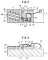
- Fig. 5 is a schematic plan view showing the internal configuration of a modulator-integrated light source module according to a second embodiment of the invention.
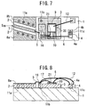
- Fig. 8 is a schematic side view showing the internal configuration of the modulator-integrated light source module according to the third embodiment of Fig. 7.
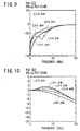
- Fig. 9 is a graph showing the frequency characteristic of the parameter S11 of the module according to the first embodiment of Fig. 3.
- Fig. 10 is a graph showing the frequency characteristic of the parameter 521 of the module according to the first embodiment of Figs. 3 and 3.
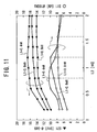
- Fig. 11 is a graph showing the variation of the parameters S11 and S21 of the module according to the first embodiment of Figs. 3 and 4 as a function of the inductance of the bonding wire.
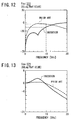
- Fig. 12 is a graph showing the frequency characteristic of the parameter S11 of the module according to the first embodiment of Figs. 3 and 4 and the prior-art module of Figs. 1 and 2.
- Fig. 13 is a graph showing the frequency characteristic of the parameter S21 of the module according to the first embodiment of Figs. 3 and 4 and the prior-art module of Figs. 1 and 2.
- a high-frequency circuit module which is a modulator-integrated light source module, comprises a block-shaped conductive base 1, a dielectric substrate 2, a heat sink 3, a modulator-integrated light source chip 20, and a matching resistor 4.
- the substrate 2, the sink 3, and the resistor 4 are mounted on the surface of the base 1.
- the substrate 2 and the resistor 4 are located at opposite sides to each other with respect to the sink 3.
- the sink 3 is apart from the substrate 2 and the resistor 4 at small distances.
- the chip 20 is mounted on the sink 3.
- the chip 20 comprises a semiconductor laser 9 and an external modulator 10.
- the resistor 4 is of the chip type or thin-film type.
- the dielectric substrate 2 is, for example, made of alumina (Al 2 O 3 ).
- the heat sink 3 serves to cool the modulator-integrated light source chip 20 mounted thereon, i.e., to dissipate the heat generated by the chip 20.
- the sink 3 is mechanically and electrically connected to the base 1 by way of a conductive via hole (e.g., a plated via hole) 11b.
- any microstrip line may be used as the transmission line for the input signal S IN into the external modulator 10.
- One end of a conductive bonding wire 6 is bonded to the bonding pad 21 of the modulator 10 of the chip 20 while the other end thereof is bonded to the other end or another terminal 4a of the resistor 4.
- the modulator 10 is electrically connected to the resistor 4 by way of the bonding wire 6.
- the terminal 4b of the resistor 4 is electrically connected to the base 11 by way of the via hole 11c.
- a high-frequency electric input signal S IN to be transmitted is applied to the signal line 7 from its opposite end to the heat sink 3.
- the signal S IN is then sent to the external modulator 10 of the modulator-integrated light source chip 20 by way of the signal line 7 and the bonding wire 5.
- the modulator 10 modulates the output light of the laser 9 with a constant intensity according to the electric signal S IN thus inputted, generating the signal light.
- the signal light thus generated is emitted from the chip 20 and the modulator-integrated light source module.
- the length of the bonding wires 5 and 6 is so determined as to satisfy the following conditions (i) and (ii).
- the laser 9 is supplied with an electric, driving current by way of a conductive bonding wire 12.
- the characteristic impedance of the combination of the external modulator 10 of the modulator-integrated light source chip 20 and the bonding wires 5 and 6 is equal to or greater than the characteristic impedance of the input side of the high-frequency electric signal S IN with respect to the same combination.
- the inductance of the bonding wire 6 is greater in value than the inductance of the bonding wire 5. Therefore, the degradation of the high-frequency characteristic of the high-frequency circuit module of the first embodiment is prevented by the use of a different method from the previously-described method of decreasing the lengths of the bonding wires 105 and 106 in the prior-art module.
- Figs. 9 and 10 show the frequency characteristic of the S parameters of the module according to the first embodiment of Figs. 3 and 4, where the inductance L2 of the bonding wire 6 was set at 0.2 nH, 0.6 nH, 1.0 nH, and 1.4 nH while the inductance L1 of the bonding wire 5 was kept at 0.6 nH.
- the parameter S11 is shown, which indicates the high-frequency reflection characteristic of the module.
- the inductance L2 of the wire 6 is 0.2 nH and 0.6 nH, which are equal to or less than the inductance L1 (0.6 nH) of the wire 5, the return loss exceeds -10 dB at the frequency of 10 GHz or higher. This means that the high-frequency reflection characteristic degrades at the frequency of 10 GHz or higher.
- the inductance L2 of the wire 6 is 1.0 nH and 1.4 nH, which are greater than the inductance L1 (0.6 nH) of the wire 5, the return loss does not exceed -10 dB. This means that the high-frequency reflection characteristic does not degrade.
- the parameter S21 is shown, which indicates the frequency response characteristic of the module.
- the inductances L1 and L2 are preferably set to satisfy the relationship of L1 ⁇ L2.
- the length of the bonding wire 5 is set to be shorter than that of the bonding wire 6.
- the length of the wire 5 is set at 0.6 mm and the length of the wire 6 is set at 1.0 mm in the module of the first embodiment.
- the value of S11 at 10 GHz was -10 dB while the -3dB region of S21 was given at 15 GHz, as seen from Figs. 9 and 10, respectively.
- Fig. 11 shows the change of the -3dB region of S21 and the value of S11 at 10 GHz as a function of the inductance L2 of the wire 6, where the inductance L1 of the wire 5 is used as a parameter.
- the inductances L1 and L2 of the wires 5 and 6 are dependent on each other. It is also seen that if the relationship of L1 ⁇ L2 is satisfied, the -3dB region of S21 is held to be approximately equal to that of the impedance matched state while the degradation of the value of S11 is effectively restrained.
- the characteristic impedance Z of the LC transmission line formed by the capacitance C of the modulator 10 and the inductances L1 and L2 of the bonding wires 5 and 6 is given by the following equation (1).
- Z L 1 - L 2 C
- the characteristic impedance Z of the LC transmission line is equal to the characteristic impedance Z 0 of the input signal line 7, the value of 521 is maximized and the value of S11 is minimized. However, in practical use, it is unnecessary that the value of S21 is maximized and the value of S11 is minimized.
- the value of S21 may not be maximized even when the value of S11 is minimized due to impedance mismatching. In this case, however, if the value of S21 exceeds a specific reference value (e.g., 14 GHz in Figs. 12 and 13), it is preferred that the value of S11 is set as small as desired.
- a specific reference value e.g. 14 GHz in Figs. 12 and 13
- Figs. 5 and 6 show a high-frequency circuit module (a modulator-integrated light source module) according to a second embodiment of the invention, which comprises the same configuration as the module according to the first embodiment of Figs. 3 and 4, except that the matching resistor 4 is located on the heat sink 3 near the signal line 7, and that a bonding pad 22 is additionally formed on the modulator 10. Therefore, the description about the same configuration is omitted here by attaching the same reference symbols as those in the first embodiment of Figs. 3 and 4 for the sake of simplification of description in Figs. 5 and 6.
- one end of the bonding wire 5 is bonded to the near end of the signal line 7 while the other end of the wire 5 is bonded to the bonding pad 21 of the external modulator 10 of the chip 20.
- the signal line 7 is electrically connected to the modulator 10 by way of the bonding wire 5. This is the same as the first embodiment.
- one end of the bonding wire 6 is bonded to the bonding pad 22 (instead of the pad 21) of the modulator 10 of the chip 20 while the other end of the wire 6 is bonded to the terminal 4a of the resistor 4.
- the modulator 10 is electrically connected to the resistor 4 by way of the bonding wire 6.
- the other terminal 4b of the resistor 4 is electrically connected to the base 11 by way of a conductive via hole 11d.
- the signal line 7 is electrically connected to the matching resistor 4 by way of the bonding wires 5 and 6 and the bonding pads 21 and 22.
- Figs. 7 and 8 show a high-frequency circuit module (a modulator-integrated light source module) according to a third embodiment of the invention, which comprises the same configuration as the module according to the first embodiment of Figs. 3 and 4, except that a conductive island 16 is additionally formed on the heat sink 3, and that the ends of the bonding wires 5 and 6 and an additional bonding wire 17 are commonly bonded to the island 16. Therefore, the description about the same ccnfiguration is omitted here by attaching the same reference symbols as those in the first embodiment of Figs. 3 and 4 for the sake of simplification of description in Figs. 7 and 8.
- the modulator 10 is electrically connected to the resistor 4 by way of the bonding wires 17 and 6 and the island 16.
- the other terminal 4b of the resistor 4 is electrically connected to the base 11 by way of the conductive via hole 11c.
- the signal line 7 is electrically connected to the matching resistor 4 by way of the bonding wires 5 and 6 and the island 16.
- the invention is not limited to the above-described first to third embodiments.
- the invention is applied to the high-frequency circuit module for optical communication.
- the invention is applicable to any circuit or any module where a signal line for transmitting a high-frequency signal is electrically connected to an element having a capacitance by way of a bonding wire or wires and at the same time, the element is electrically connected to a matching resistor for impedance matching by way of another bonding wire or wires.
- the module of the invention is incorporated into a modulation section of an optical communication device or a electrical communication device (e.g., a portable phone), a communication device having excellent high-frequency characteristics is realized.
Landscapes
- Physics & Mathematics (AREA)
- Nonlinear Science (AREA)
- General Physics & Mathematics (AREA)
- Optics & Photonics (AREA)
- Optical Modulation, Optical Deflection, Nonlinear Optics, Optical Demodulation, Optical Logic Elements (AREA)
- Wire Bonding (AREA)
- Emergency Protection Circuit Devices (AREA)
Abstract
Description
- wherein a characteristic impedance of combination of the element and the first and second bonding wires is equal to or greater than that of input side of the electric signal with respect to the combination;
- and wherein an inductance of the second wire is greater than that of the first wire.
Claims (15)
- A high-frequency circuit comprising:(a) an electronic element having a capacitance;(b) a signal line for transmitting a high-frequency electric signal to the element;(c) a terminating resistor for impedance matching;(d) a first bonding wire for electrically connecting the signal line and the element; and(e) a second bonding wire for electrically connecting the element and the resistor;wherein a characteristic impedance of combination of the element and the first and second bonding wires is equal to or greater than that of input side of the electric signal with respect to the combination;and wherein an inductance of the second wire is greater than that of the first wire.
- The circuit according to claim 1, wherein the element has a conductive pad;
and wherein the element and the first wire are electrically connected to each other at the pad while the element and the second wire are electrically connected each other at the same pad. - The circuit according to claim 1, wherein the element has a first conductive pad and a second conductive pad;
and wherein the element and the first wire are electrically connected to each other at the first pad while the element and the second wire are electrically connected to each other at the second pad. - The circuit according to claim 1, further comprising a conductive island electrically connected to the element by way of a third bonding wire;wherein the signal line is electrically connected to the island by way of the first wire, thereby electrically connecting the signal line to the element by way of the first and third wires;and wherein the resistor is electrically connected to the island by way of the second wire, thereby electrically connecting the resistor to the element by way of the second and third wires.
- The circuit according to claim 1, wherein the element is a modulator for generating an electric or optical signal by modulation according to the electric signal transmitted through the signal line.
- The circuit according to claim 1, wherein the inductance of the second wire is approximately twice in value the inductance of the first wire.
- A high-frequency circuit module comprising:(a) a base; and(b) the high-frequency circuit according to claim 1 mounted on the base.
- The module according to claim 7, wherein the element has a conductive pad;
and wherein the element and the first wire are electrically connected to each other at the pad while the element and the second wire are electrically connected each other at the same pad. - The module according to claim 7, wherein the element has a first conductive pad and a second conductive pad;
and wherein the element and the first wire are electrically connected to each other at the first pad while the element and the second wire are electrically connected to each other at the second pad. - The module according to claim 7, further comprising a conductive island electrically connected to the element by way of a third bonding wire;wherein the signal line is electrically connected to the island by way of the first wire, thereby electrically connecting the signal line to the element by way of the first and third wires;and wherein the resistor is electrically connected to the island by way of the second wire, thereby electrically connecting the resistor to the element by way of the second and third wires.
- The module according to claim 7, wherein the element is a modulator for generating an electric or optical signal by modulation according to the electric signal transmitted through the signal line.
- The module according to claim 7, wherein the inductance of the second wire is approximately twice in value the inductance of the first wire.
- The module according to claim 7, wherein the element is mounted on a heat sink fixed to the base and the signal line is located on a dielectric layer formed on the base;
and wherein the resistor is fixed directly on the base. - The module according to claim 7, wherein the element is mounted on a heat sink fixed to the base and the signal line is located on a dielectric layer formed on the base;
and wherein the resistor is fixed on the sink. - A communication device comprising the module according to claim 7.
Applications Claiming Priority (2)
| Application Number | Priority Date | Filing Date | Title |
|---|---|---|---|
| JP2000126102A JP4290314B2 (en) | 2000-04-26 | 2000-04-26 | High-frequency circuit, module mounted with the same, and communication device |
| JP2000126102 | 2000-04-26 |
Publications (2)
| Publication Number | Publication Date |
|---|---|
| EP1158340A2 true EP1158340A2 (en) | 2001-11-28 |
| EP1158340A3 EP1158340A3 (en) | 2003-11-19 |
Family
ID=18635942
Family Applications (1)
| Application Number | Title | Priority Date | Filing Date |
|---|---|---|---|
| EP20010110239 Withdrawn EP1158340A3 (en) | 2000-04-26 | 2001-04-25 | High-frequency circuit and its module for communication devices |
Country Status (4)
| Country | Link |
|---|---|
| US (1) | US6507111B2 (en) |
| EP (1) | EP1158340A3 (en) |
| JP (1) | JP4290314B2 (en) |
| CA (1) | CA2345175A1 (en) |
Cited By (1)
| Publication number | Priority date | Publication date | Assignee | Title |
|---|---|---|---|---|
| EP1617279A1 (en) * | 2004-07-12 | 2006-01-18 | OpNext Japan, Inc. | Optical module |
Families Citing this family (15)
| Publication number | Priority date | Publication date | Assignee | Title |
|---|---|---|---|---|
| JP2001209017A (en) * | 1999-11-15 | 2001-08-03 | Mitsubishi Electric Corp | Photoelectric conversion semiconductor device |
| JP2003521127A (en) * | 2000-01-28 | 2003-07-08 | エリクソン インコーポレイテッド | Multiple earth signal path LDMOS power package |
| US6881623B2 (en) * | 2001-08-29 | 2005-04-19 | Micron Technology, Inc. | Method of forming chalcogenide comprising devices, method of forming a programmable memory cell of memory circuitry, and a chalcogenide comprising device |
| JP3975786B2 (en) * | 2002-03-12 | 2007-09-12 | 日本電気株式会社 | Optical modulator excitation circuit |
| JP2004170931A (en) * | 2002-11-05 | 2004-06-17 | Ngk Insulators Ltd | Optical modulator |
| US7228014B2 (en) * | 2004-03-11 | 2007-06-05 | Avanex Corporation | System for reducing the electrical return loss of a lithium niobate traveling wave optical modulator with low characteristic impedance |
| JP4685410B2 (en) * | 2004-11-01 | 2011-05-18 | 日本オプネクスト株式会社 | Optical module |
| US7011458B2 (en) | 2004-07-12 | 2006-03-14 | Opnext Japan, Inc. | Optical module |
| JP4815814B2 (en) * | 2005-02-04 | 2011-11-16 | 三菱電機株式会社 | Optical module |
| JP2007208671A (en) * | 2006-02-02 | 2007-08-16 | Mitsubishi Electric Corp | Package for microwave module |
| JP4856465B2 (en) | 2006-04-19 | 2012-01-18 | 日本オプネクスト株式会社 | Optical semiconductor element mounting substrate and optical transmission module |
| SG169241A1 (en) * | 2009-08-12 | 2011-03-30 | Sony Corp | An integrated circuit |
| JP6926562B2 (en) | 2017-03-21 | 2021-08-25 | 住友電気工業株式会社 | Light modulator module |
| JP7124741B2 (en) | 2019-02-06 | 2022-08-24 | 日本電信電話株式会社 | optical transmitter |
| CN112186496B (en) * | 2020-09-22 | 2022-05-13 | 武汉光迅科技股份有限公司 | Impedance matching method and laser module |
Family Cites Families (12)
| Publication number | Priority date | Publication date | Assignee | Title |
|---|---|---|---|---|
| US4686492A (en) * | 1985-03-04 | 1987-08-11 | Tektronix, Inc. | Impedance match connection using multiple layers of bond wires |
| JP2954422B2 (en) * | 1992-05-22 | 1999-09-27 | 株式会社日立製作所 | Optical transmission module |
| JP3553222B2 (en) * | 1995-09-20 | 2004-08-11 | 三菱電機株式会社 | Optical modulator module |
| KR0156334B1 (en) * | 1995-10-14 | 1998-10-15 | 김광호 | Semiconductor chip package having shield bonding wire for high frequency and high density |
| FR2747802B1 (en) * | 1996-04-18 | 1998-05-15 | Commissariat Energie Atomique | OPTOMECHANICAL MICRODISPOSITIVE, AND APPLICATION TO AN OPTOMECHANICAL MICRODEFLECTOR |
| JPH1051069A (en) * | 1996-07-29 | 1998-02-20 | Mitsubishi Electric Corp | Optical semiconductor device |
| KR0181896B1 (en) * | 1996-09-14 | 1999-05-15 | 삼성전자주식회사 | Wide-band device of fast optical module |
| JPH10275957A (en) | 1997-03-31 | 1998-10-13 | Hitachi Ltd | Optical semiconductor chip carrier |
| US6434726B1 (en) * | 1999-06-29 | 2002-08-13 | Lucent Technologies Inc. | System and method of transmission using coplanar bond wires |
| JP3539549B2 (en) * | 1999-09-20 | 2004-07-07 | シャープ株式会社 | Semiconductor device |
| US6806988B2 (en) * | 2000-03-03 | 2004-10-19 | Canon Kabushiki Kaisha | Optical apparatus |
| JP3898438B2 (en) * | 2000-11-22 | 2007-03-28 | 株式会社リコー | Lens tilt device |
-
2000
- 2000-04-26 JP JP2000126102A patent/JP4290314B2/en not_active Expired - Fee Related
-
2001
- 2001-04-25 EP EP20010110239 patent/EP1158340A3/en not_active Withdrawn
- 2001-04-25 US US09/842,243 patent/US6507111B2/en not_active Expired - Lifetime
- 2001-04-25 CA CA 2345175 patent/CA2345175A1/en not_active Abandoned
Cited By (2)
| Publication number | Priority date | Publication date | Assignee | Title |
|---|---|---|---|---|
| EP1617279A1 (en) * | 2004-07-12 | 2006-01-18 | OpNext Japan, Inc. | Optical module |
| CN100347916C (en) * | 2004-07-12 | 2007-11-07 | 日本光进株式会社 | Optical module |
Also Published As
| Publication number | Publication date |
|---|---|
| US20010038146A1 (en) | 2001-11-08 |
| US6507111B2 (en) | 2003-01-14 |
| JP2001308130A (en) | 2001-11-02 |
| EP1158340A3 (en) | 2003-11-19 |
| JP4290314B2 (en) | 2009-07-01 |
| CA2345175A1 (en) | 2001-10-26 |
Similar Documents
| Publication | Publication Date | Title |
|---|---|---|
| EP1158340A2 (en) | High-frequency circuit and its module for communication devices | |
| EP1617279B1 (en) | Optical module | |
| JP5313730B2 (en) | Optical transmitter and optical transmission module | |
| US6181718B1 (en) | Electronically cooled semiconductor laser module with modified ground line inductance | |
| US12265286B2 (en) | Broadband electro-absorption optical modulator using on-chip RF input signal termination | |
| US20030156608A1 (en) | Laser-diode module, optical transceiver and fiber transmission system | |
| JP2001257412A (en) | Optical transmission module | |
| EP1655630A2 (en) | Optical module | |
| JP7468846B2 (en) | Optical semiconductor device and carrier | |
| US7167494B2 (en) | Optical transmission module | |
| JP2004319984A (en) | Optical module with TO-CAN structure | |
| US5926308A (en) | High-speed optical modulator module | |
| US20020105395A1 (en) | DC block circuit and communication equipment | |
| US20230139615A1 (en) | Optical Semiconductor Chip | |
| JP2004093606A (en) | Optical module and optical transmitter | |
| US7553092B2 (en) | Optical module and optical module package | |
| JP3916072B2 (en) | AC coupling circuit | |
| JP4105647B2 (en) | Semiconductor laser module and optical transmitter | |
| JP2005191347A (en) | Chip carrier for semiconductor optical device, optical module, and optical transceiver | |
| JP7622397B2 (en) | Optical Semiconductor Module | |
| US12567719B2 (en) | Optical semiconductor chip | |
| US20210359761A1 (en) | Optical semiconductor device, optical transmission module, and optical transceiver | |
| JP2004259880A (en) | Optical semiconductor device | |
| JP4734310B2 (en) | Chip carrier for semiconductor optical device, optical module, and optical transceiver | |
| JP2004281975A (en) | Optical semiconductor device |
Legal Events
| Date | Code | Title | Description |
|---|---|---|---|
| PUAI | Public reference made under article 153(3) epc to a published international application that has entered the european phase |
Free format text: ORIGINAL CODE: 0009012 |
|
| AK | Designated contracting states |
Kind code of ref document: A2 Designated state(s): AT BE CH CY DE DK ES FI FR GB GR IE IT LI LU MC NL PT SE TR |
|
| AX | Request for extension of the european patent |
Free format text: AL;LT;LV;MK;RO;SI |
|
| RAP1 | Party data changed (applicant data changed or rights of an application transferred) |
Owner name: NEC ELECTRONICS CORPORATION |
|
| PUAL | Search report despatched |
Free format text: ORIGINAL CODE: 0009013 |
|
| AK | Designated contracting states |
Kind code of ref document: A3 Designated state(s): AT BE CH CY DE DK ES FI FR GB GR IE IT LI LU MC NL PT SE TR |
|
| AX | Request for extension of the european patent |
Extension state: AL LT LV MK RO SI |
|
| 17P | Request for examination filed |
Effective date: 20031014 |
|
| STAA | Information on the status of an ep patent application or granted ep patent |
Free format text: STATUS: THE APPLICATION HAS BEEN WITHDRAWN |
|
| 18W | Application withdrawn |
Effective date: 20031217 |