EP1157783A2 - Polishing method and polishing apparatus - Google Patents
Polishing method and polishing apparatus Download PDFInfo
- Publication number
- EP1157783A2 EP1157783A2 EP01113008A EP01113008A EP1157783A2 EP 1157783 A2 EP1157783 A2 EP 1157783A2 EP 01113008 A EP01113008 A EP 01113008A EP 01113008 A EP01113008 A EP 01113008A EP 1157783 A2 EP1157783 A2 EP 1157783A2
- Authority
- EP
- European Patent Office
- Prior art keywords
- polishing
- top ring
- turntable
- semiconductor wafer
- polished
- Prior art date
- Legal status (The legal status is an assumption and is not a legal conclusion. Google has not performed a legal analysis and makes no representation as to the accuracy of the status listed.)
- Granted
Links
Images


Classifications
-
- B—PERFORMING OPERATIONS; TRANSPORTING
- B24—GRINDING; POLISHING
- B24B—MACHINES, DEVICES, OR PROCESSES FOR GRINDING OR POLISHING; DRESSING OR CONDITIONING OF ABRADING SURFACES; FEEDING OF GRINDING, POLISHING, OR LAPPING AGENTS
- B24B37/00—Lapping machines or devices; Accessories
- B24B37/04—Lapping machines or devices; Accessories designed for working plane surfaces
- B24B37/042—Lapping machines or devices; Accessories designed for working plane surfaces operating processes therefor
-
- B—PERFORMING OPERATIONS; TRANSPORTING
- B24—GRINDING; POLISHING
- B24B—MACHINES, DEVICES, OR PROCESSES FOR GRINDING OR POLISHING; DRESSING OR CONDITIONING OF ABRADING SURFACES; FEEDING OF GRINDING, POLISHING, OR LAPPING AGENTS
- B24B49/00—Measuring or gauging equipment for controlling the feed movement of the grinding tool or work; Arrangements of indicating or measuring equipment, e.g. for indicating the start of the grinding operation
-
- H—ELECTRICITY
- H10—SEMICONDUCTOR DEVICES; ELECTRIC SOLID-STATE DEVICES NOT OTHERWISE PROVIDED FOR
- H10P—GENERIC PROCESSES OR APPARATUS FOR THE MANUFACTURE OR TREATMENT OF DEVICES COVERED BY CLASS H10
- H10P52/00—Grinding, lapping or polishing of wafers, substrates or parts of devices
Definitions
- the present invention relates to a polishing method and apparatus, and more particularly to a polishing method and apparatus for polishing a workpiece such as a semiconductor wafer to a flat mirror finish.
- CMP Chemical Mechanical Polishing
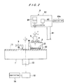
- FIG. 1 is a schematic view showing the basic structure of this type of polishing apparatus.
- the polishing apparatus has a turntable 1 with a polishing cloth 11 attached thereon and constituting a polishing surface, and a top ring 2 for holding a semiconductor wafer (workpiece) W in such a manner that the surface, to be polished, of the semiconductor wafer W faces the turntable 1.
- the top ring 2 is connected to a lower end of a top ring shaft 3 via a ball joint 4 so as to be tiltable with respect to the top ring shaft 3.
- the semiconductor wafer W to be polished is pressed against the turntable 1 under a certain pressure by the top ring 2 while the turntable 1 and the top ring 2 are independently being rotated, and the surface of the semiconductor wafer W is polished to a flat mirror finish while a polishing liquid Q is being supplied from a polishing liquid supply nozzle 5.
- the surface, to be polished, of the semiconductor wafer W is brought into sliding contact with the upper surface of the polishing cloth 11 while following the inclination of the upper surface of the polishing cloth 11 via the ball joint 4.
- a polishing cloth made of non-woven fabric As a polishing cloth attached on a turntable, a polishing cloth made of non-woven fabric has heretofore been employed. Higher levels of integration achieved in recent years for ICs and LSI circuits demand smaller steps or surface irregularities on the polished surface of the semiconductor wafer. In order to meet such a demand, there has been used a polishing cloth made of a hard material such as polyurethane foam.
- the polishing apparatus After the semiconductor wafer W is polished by the polishing apparatus, it is necessary to remove the semiconductor wafer W from the polishing surface (the polishing cloth 11) on the turntable 1. However, a large surface tension acts between the polishing cloth 11 and the semiconductor wafer W due to the polishing liquid Q interposed therebetween. Accordingly, if the top ring 2 holding the semiconductor wafer W is lifted at the polishing position in order to remove the semiconductor wafer W from the polishing cloth 11, there are some cases that only the top ring 2 is lifted and the semiconductor wafer W adheres to the polishing cloth 11 to be left on the polishing cloth 11.
- Such a problem can be solved by an overhanging action of the top ring.
- the overhanging action after the polishing process is completed, the top ring 2 is not lifted at the polishing position, but is moved to the outer circumferential edge of the polishing cloth 11 to partly expose the polished surface of the semiconductor wafer W beyond the outer circumferential edge of the polishing cloth 11 and then lifted to remove the semiconductor wafer W from the polishing cloth 11.
- This overhanging action allows the surface tension between the polishing cloth 11 and the semiconductor wafer W to be reduced, and the semiconductor wafer W can reliably be separated or removed from the polishing cloth 11.
- the surface tension between the polishing cloth 11 and the semiconductor wafer W can be reduced.
- the top ring 2 may tilt when the polished semiconductor wafer W projects from the outer circumferential edge of the polishing cloth 11. In this case, the semiconductor wafer W is intensively pressed at the outer circumferential edge of the polishing cloth 11, so that the semiconductor wafer W is cracked or scratched.
- polishing capability of the polishing cloth is gradually deteriorated due to a deposit of abrasive particles and ground-off particles of the semiconductor material, and due to changes in the characteristics of the polishing cloth. Therefore, if the same polishing cloth is used to repeatedly polish semiconductor wafers, the polishing rate of the polishing apparatus is lowered, and the polished semiconductor wafers tend to suffer polishing irregularities. Therefore, it has been customary to condition the polishing cloth according to a process called "dressing" for recovering the surface of the polishing cloth with a diamond dresser or the like before, or after, or during polishing.
- the diamond dresser dresses the polishing surface of the polishing cloth 11, it scrapes a thin layer off the polishing cloth 11. Therefore, after the polishing surface of the polishing cloth has been dressed many times, it becomes irregular, i.e., loses its planarity, causing formation of steps. As a result, during the movement of the polished semiconductor wafer W to the outer circumferential edge of the polishing cloth 11 in the aforementioned overhanging action, the semiconductor wafer W may be cracked or scratched because of the irregularities of the polishing cloth 11.
- the present invention has been made in view of the above drawbacks. It is therefore an object of the present invention to provide a polishing method and apparatus which can easily and safely remove a polished workpiece from a polishing surface, and can increase a throughput.
- a polishing method comprising: rotating a turntable having a polishing surface thereon, and a top ring for holding a workpiece to be polished, respectively; pressing a surface, to be polished, of the workpiece held by the top ring against the polishing surface on the turntable to polish the workpiece; and increasing a relative speed of the turntable and the top ring when the polished workpiece held by the top ring is to be removed from the polishing surface on the turntable, in comparison with a relative speed of the turntable and the top ring at a period of polishing.
- a rotational speed of the turntable is increased in comparison with a rotational speed of the turntable at a period of polishing to increase the relative speed of the turntable and the top ring.
- rotational speeds of the turntable and the top ring are respectively increased in comparison with rotational speeds of the turntable and the top ring at a period of polishing to increase the relative speed of the turntable and the top ring.
- a polishing apparatus for polishing a workpiece to be polished, comprising: a turntable having a polishing surface thereon; a top ring for holding the workpiece to be polished and pressing the workpiece against the polishing surface on the turntable; a motor for rotating the turntable; and a controller for controlling a rotational speed of the motor; wherein when the polished workpiece held by the top ring is to be removed from the polishing surface on the turntable, the motor increases a rotational speed of the turntable in comparison with a rotational speed of the turntable at a period of polishing.
- a polishing apparatus for polishing a workpiece to be polished, comprising: a turntable having a polishing surface thereon; a top ring for holding the workpiece to be polished and pressing the workpiece against the polishing surface on the turntable; a motor for rotating the top ring; and a controller for controlling a rotational speed of the motor; wherein when the polished workpiece held by the top ring is to be removed from the polishing surface on the turntable, the motor increases a rotational speed of the top ring in comparison with a rotational speed of the top ring at a period of polishing.
- a polishing method comprising: moving a polishing surface and a top ring for holding a workpiece to be polished relative to each other; pressing a surface, to be polished, of the workpiece held by the top ring against the polishing surface to polish the workpiece; and increasing a relative speed of the polishing surface and the top ring when the polished workpiece held by the top ring is to be removed from the polishing surface, in comparison with a relative speed of the polishing surface and the top ring at a period of polishing.
- the rotational speed of the turntable be increased to 100 min -1 or larger, and the rotational speed of the top ring be increased to 75 min -1 or larger.
- the liquid film thickness of a polishing liquid on the polishing surface is decreased by the action of the centrifugal force, so that the surface tension due to the polishing liquid is reduced. Therefore, even if the top ring is lifted at the polishing position without an overhanging action, the workpiece can easily be removed from the polishing surface.
- the present invention can prevent the workpiece from being left on the polishing surface and being cracked or scratched. Further, since it is not necessary to perform the overhanging action, tact time for polishing can be reduced to increase a throughput.
- the rotational speed of the turntable is increased, the components of the polishing liquid are scattered and discharged from the upper surface of the turntable by the action of the centrifugal force. Accordingly, it becomes easier to remove the workpiece from the polishing surface, and simultaneously the polishing conditions for the next workpiece to be polished can be arranged to be preferred conditions. As a result, the throughput can be increased.
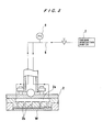
- FIG. 2 is a front view showing the whole structure of a polishing apparatus according to an embodiment of the present invention.
- like parts and components are designated by the same reference numerals and characters as those shown in FIG. 1.
- the polishing apparatus comprises a turntable 1, a polishing liquid supply nozzle 5, and a top ring unit 6.
- the turntable 1 has a vertical shaft 13 coupled to a motor 12 disposed below the turntable 1 and is rotatable about the shaft 13, as indicated by an arrow in FIG. 1.
- the motor 12 is connected to a controller 14 for controlling a rotational speed of the motor 12.
- a polishing cloth 11 is attached on an upper surface of the turntable 1.
- the polishing cloth 11 has an upper polishing surface held in sliding contact with a semiconductor wafer W (workpiece) to be polished.
- the polishing liquid supply nozzle 5 is disposed above the turntable 1, and a polishing liquid Q is supplied onto the polishing cloth 11 of the turntable 1 from the polishing liquid supply nozzle 5.
- the turntable 1 has the polishing cloth 11 attached thereon.
- the turntable 1 is not limited to the above one, and the turntable 1 may comprise a polishing plate of a fixed abrasive, for example.
- the fixed abrasive comprises abrasive particles fixed by a binder.
- the top ring unit 6 mainly comprises a swing shaft 61, an arm-shaped top ring head 62 connected to the swing shaft 61, and a top ring 2 connected to a top ring shaft 3 extended downwardly from the top ring head 62.
- the top ring head 62 is swingable in a horizontal plane by rotation of the swing shaft 61.
- the top ring 2 is connected to the lower end of the top ring shaft 3 via a ball joint 4 so as to be tiltable with respect to the top ring shaft 3.
- the top ring 2 of the top ring unit 6 has, on a lower surface thereof, an elastic pad 21 formed of polyurethane or the like.
- the semiconductor wafer W is attracted to a lower surface of the elastic pad 21 under a vacuum in such a state that the semiconductor wafer W is brought into contact with the lower surface of the elastic pad 21, so that the semiconductor wafer W is held by the top ring 2.
- the top ring 2 has a cylindrical guide ring 22 at an outer circumferential edge of a lower portion thereof. A lower portion of the guide ring 22 protrudes from the top ring 2, and hence a recess is formed at the radially inner side of the lower portion of the guide ring 22.
- the semiconductor wafer W is held in the recess for preventing the semiconductor wafer W from being dislodged from the lower surface of the top ring 2 during the polishing process.
- the top ring 2 is coupled to a motor 63 provided in the top ring head 62 via the top ring shaft 3, and is rotatable about the top ring shaft 3.
- the motor 63 is connected to a controller 63a for controlling a rotational speed of the motor 63.
- the top ring 2 is also coupled to a lifting/lowering cylinder 64 via the top ring shaft 3, and is vertically movable for pressing the semiconductor wafer W held in the top ring 2 against the polishing cloth 11 under a predetermined pressure.
- the semiconductor wafer W held on the lower surface of the elastic pad 21 attached on the lower surface of the top ring 2 is pressed against the polishing cloth 11 on the turntable 1, while the polishing liquid Q is being supplied onto the polishing cloth 11 of the turntable 1 from the polishing liquid supply nozzle 5.
- the turntable 1 and the top ring 2 are independently rotated, so that the polishing cloth 11 and the semiconductor wafer W are moved relative to each other.
- a suspension of fine polishing particles of silica or the like in an alkali solution is used as the polishing liquid supplied from the polishing liquid nozzle 5.
- the semiconductor wafer W is polished to a flat mirror finish by the combined effect of a chemical polishing effect attained by the alkali and a mechanical polishing effect attained by the polishing particles.
- the semiconductor wafer W is polished in the above manner. After the polishing process of the semiconductor wafer W is completed, it is necessary to separate or remove the semiconductor wafer W from the polishing cloth 11 on the turntable 1. In this case, the surface tension acts between the polishing cloth 11 and the semiconductor wafer W, as described above. According to the present invention, when the semiconductor wafer W is to be separated or removed from the polishing cloth 11, the rotational speeds of the turntable 1 and the top ring 2 are increased by the motor 12 and the motor 63 in comparison with their rotational speeds at a period of the polishing process.
- the present invention can prevent the semiconductor wafer W from being left on the polishing cloth 11 and being cracked or scratched. Further, since it is not necessary to perform the overhanging action, tact time for polishing can be reduced to increase a throughput.
- the rotational speed of the turntable 1 is increased by the motor 12, the components of the polishing liquid are scattered and discharged from the upper surface of the turntable 1 by the action of the centrifugal force. Accordingly, it becomes easier to remove the semiconductor wafer from the polishing surface, and simultaneously the polishing conditions for the next semiconductor wafer to be polished can be arranged to be preferred conditions. As a result, the throughput can be increased.
- a vacuum line 8 communicating with a vacuum evacuation source 7 is connected to the top ring 2.
- the top ring 2 has a chamber (or a space) 2a connected to the vacuum line 8, and a plurality of holes 2b communicating with the chamber 2a and being open to the lower surface of the top ring 2.
- the semiconductor wafer W is held on the lower surface of the top ring 2 by vacuum attraction.
- the top ring 2 is mechanically lifted. If the semiconductor wafer W is dislodged from the top ring 2 and is left on the polishing cloth 11, the pressure of the vacuum line 8 changes from a vacuum nearer to the atmospheric pressure. Therefore, the pressure of the vacuum line 8 is monitored to judge whether the semiconductor wafer W has normally been removed from the polishing cloth 11 or not.
- a vacuum pressure sensor 9 is provided in the vacuum line 8 to measure and monitor the pressure of the vacuum line 8, for thereby judging whether the semiconductor wafer W has normally been removed from the polishing cloth 11 or not. Specifically, after the lifting operation of the top ring 2 is started, the pressure of the vacuum line 8 is measured with the vacuum pressure sensor 9. If the measured value is less than a predetermined pressure value, it is judged that the semiconductor wafer W has normally been removed from the polishing cloth 11 in such a state that the semiconductor wafer W is attracted to the top ring 2.
- the top ring 2 is lifted at the polishing position without an overhanging action.
- the top ring 2 may perform an overhanging action after the polishing process, as shown in FIGS. 4A and 4B.
- the top ring 2 is moved to the outer circumferential edge of the polishing cloth 11 to partly expose the polished surface of the semiconductor wafer W beyond the outer circumferential edge of the polishing cloth 11 and then lifted to remove the semiconductor wafer W from the polishing cloth 11.
- the rotational speed of the top ring 2 is increased in comparison with the rotational speed at a period of the polishing process.
- the liquid film thickness of the polishing liquid on the polishing cloth 11 is decreased by the action of the centrifugal force, so that the surface tension due to the polishing liquid is reduced by the synergistic effect of the centrifugal force and the overhanging action. Therefore, the semiconductor wafer W can more easily be removed from the polishing surface. As a result, the semiconductor wafer W can be prevented from being left on the polishing surface 18 more effectively.
- the polishing surface is rotated to polish the semiconductor wafer.
- the polishing surface and the top ring may be moved relative to each other.
- a polishing surface is constituted by a belt 15 having abrasive particles on its surface.
- the belt 15 is wound on two rotatable drums 16, 17.
- the drums 16, 17 are rotated to linearly move the belt 15 along an arrow A.
- a support 18 is disposed between an upper belt surface 15a and a lower belt surface 15b.
- a semiconductor wafer held by the top ring 2 is pressed against the belt 15 and the support 18.
- the semiconductor wafer is polished.
- the rotational speed of the top ring 2 is increased in comparison with the rotational speed at a period of the polishing process.
- the semiconductor wafer can be prevented from being left on the belt 15 (polishing surface).
- a rotational speed of the turntable is increased in comparison with a rotational speed of the turntable at a period of polishing.
- a relative speed of the turntable and the top ring is increased in comparison with a relative speed of the turntable and the top ring at a period of polishing.
- tact time for polishing can be reduced to increase a throughput. Furthermore, when the rotational speed of the turntable is increased, the components of the polishing liquid are scattered and discharged from the upper surface of the turntable by the action of the centrifugal force. Accordingly, it becomes easier to remove the workpiece from the polishing surface, and simultaneously the polishing conditions for the next workpiece to be polished can be arranged to be preferred conditions. As a result, the throughput can be increased.
Landscapes
- Engineering & Computer Science (AREA)
- Mechanical Engineering (AREA)
- Finish Polishing, Edge Sharpening, And Grinding By Specific Grinding Devices (AREA)
- Mechanical Treatment Of Semiconductor (AREA)
Abstract
Description
Specifically, when the rotational speeds of the
A strain gauge was provided in the top ring, and the rotational speeds of the turntable and the top ring were respectively changed when the semiconductor wafer was to be removed from the polishing cloth. An axial force acting on the top ring at this time, i.e., a force for lifting the top ring, was measured.
- A top ring for holding a semiconductor wafer having a diameter of 200 mm was used.
- Dressing was performed for 600 seconds by a dresser before a polishing process.
- After three semiconductor wafers were polished as dummies to obtain the normal condition of the polishing cloth, two semiconductor wafers were polished for measuring a force for lifting the top ring. The force for lifting the top ring was calculated based on the average of the values measured after polishing of the two semiconductor wafers.
- During the polishing process, the rotational speed of the turntable was 22 min-1, and the rotational speed of the top ring was 16 min-1.
- When the semiconductor wafer was lifted, the rotational speed of the turntable was changed to 50 min-1, 75 min-1 or 100 min-1, and the rotational speed of the top ring was changed to 55 min-1 or 75 min-1.
- As the dresser, a new dresser and a used dresser that had already used for processing 17,000 semiconductor wafers were used in the experiments, respectively.
| Rotational speed of turntable (min-1) | Rotational speed of top ring (min-1) | Force for lifting top ring in the case of new dresser (N) | Force for lifting top ring in the case of used dresser (N) |
| 50 | 55 | 332.1 | 342 |
| 75 | 55 | 99.9 | 378.9 |
| 100 | 55 | 378 | 185.4 |
| 50 | 75 | 389.7 | 300.9 |
| 75 | 75 | 338.7 | 178.8 |
| 100 | 75 | 25.9 | 96.6 |
Claims (11)
- A polishing method comprising:rotating a turntable having a polishing surface thereon, and a top ring for holding a workpiece to be polished, respectively;pressing a surface, to be polished, of said workpiece held by said top ring against said polishing surface on said turntable to polish said workpiece; andincreasing a relative speed of said turntable and said top ring when said polished workpiece held by said top ring is to be removed from said polishing surface on said turntable, in comparison with a relative speed of said turntable and said top ring at a period of polishing.
- A polishing method according to claim 1, wherein a rotational speed of said turntable is increased in comparison with a rotational speed of said turntable at a period of polishing to increase said relative speed of said turntable and said top ring.
- A polishing method according to claim 2, wherein said rotational speed of said turntable is increased to 100 min-1 or larger.
- A polishing method according to claim 1, wherein rotational speeds of said turntable and said top ring are respectively increased in comparison with rotational speeds of said turntable and said top ring at a period of polishing to increase said relative speed of said turntable and said top ring.
- A polishing method according to claim 4, wherein said rotational speed of said top ring is increased to 75 min-1 or larger.
- A polishing method according to claim 5, wherein said rotational speed of said turntable is increased to 100 min-1 or larger.
- A polishing apparatus for polishing a workpiece to be polished, comprising:a turntable having a polishing surface thereon;a top ring for holding said workpiece to be polished and pressing said workpiece against said polishing surface on said turntable;a motor for rotating said turntable; anda controller for controlling a rotational speed of said motor;wherein when said polished workpiece held by said top ring is to be removed from said polishing surface on said turntable, said motor increases a rotational speed of said turntable in comparison with a rotational speed of said turntable at a period of polishing.
- A polishing apparatus according to claim 7, wherein said motor increases said rotational speed of said turntable to 100 min-1 or larger.
- A polishing apparatus for polishing a workpiece to be polished, comprising:a turntable having a polishing surface thereon;a top ring for holding said workpiece to be polished and pressing said workpiece against said polishing surface on said turntable;a motor for rotating said top ring; anda controller for controlling a rotational speed of said motor;wherein when said polished workpiece held by said top ring is to be removed from said polishing surface on said turntable, said motor increases a rotational speed of said top ring in comparison with a rotational speed of said top ring at a period of polishing.
- A polishing apparatus according to claim 9, wherein said motor increases said rotational speed of said top ring to 75 min-1 or larger.
- A polishing method comprising:moving a polishing surface and a top ring for holding a workpiece to be polished relative to each other;pressing a surface, to be polished, of said workpiece held by said top ring against said polishing surface to polish said workpiece; andincreasing a relative speed of said polishing surface and said top ring when said polished workpiece held by said top ring is to be removed from said polishing surface, in comparison with a relative speed of said polishing surface and said top ring at a period of polishing.
Applications Claiming Priority (2)
| Application Number | Priority Date | Filing Date | Title |
|---|---|---|---|
| JP2000156690A JP2001334458A (en) | 2000-05-26 | 2000-05-26 | Polishing method |
| JP2000156690 | 2000-05-26 |
Publications (3)
| Publication Number | Publication Date |
|---|---|
| EP1157783A2 true EP1157783A2 (en) | 2001-11-28 |
| EP1157783A3 EP1157783A3 (en) | 2003-10-15 |
| EP1157783B1 EP1157783B1 (en) | 2010-01-06 |
Family
ID=18661445
Family Applications (1)
| Application Number | Title | Priority Date | Filing Date |
|---|---|---|---|
| EP01113008A Expired - Lifetime EP1157783B1 (en) | 2000-05-26 | 2001-05-28 | Polishing method and polishing apparatus |
Country Status (6)
| Country | Link |
|---|---|
| US (1) | US6746312B2 (en) |
| EP (1) | EP1157783B1 (en) |
| JP (1) | JP2001334458A (en) |
| KR (1) | KR100777342B1 (en) |
| DE (1) | DE60140982D1 (en) |
| TW (1) | TW577784B (en) |
Families Citing this family (9)
| Publication number | Priority date | Publication date | Assignee | Title |
|---|---|---|---|---|
| JP4323129B2 (en) * | 2002-02-15 | 2009-09-02 | 株式会社ディスコ | Plate-like material transport mechanism |
| JP2004193289A (en) * | 2002-12-10 | 2004-07-08 | Ebara Corp | Polishing method |
| US6908366B2 (en) * | 2003-01-10 | 2005-06-21 | 3M Innovative Properties Company | Method of using a soft subpad for chemical mechanical polishing |
| CN100551623C (en) * | 2003-01-10 | 2009-10-21 | 3M创新有限公司 | Pad structure for chemical mechanical planarization |
| JP4086722B2 (en) * | 2003-06-24 | 2008-05-14 | 株式会社荏原製作所 | Substrate holding device and polishing device |
| US7338569B2 (en) * | 2004-09-29 | 2008-03-04 | Agere Systems Inc. | Method and system of using offset gage for CMP polishing pad alignment and adjustment |
| JP5248127B2 (en) * | 2008-01-30 | 2013-07-31 | 株式会社荏原製作所 | Polishing method and polishing apparatus |
| CN108466131A (en) * | 2018-05-30 | 2018-08-31 | 四川欧瑞特光电科技有限公司 | A kind of optical element process equipment |
| CN114161246A (en) * | 2021-12-28 | 2022-03-11 | 唐山万士和电子有限公司 | Convex wafer workpiece grinding device |
Family Cites Families (6)
| Publication number | Priority date | Publication date | Assignee | Title |
|---|---|---|---|---|
| US5658190A (en) * | 1995-12-15 | 1997-08-19 | Micron Technology, Inc. | Apparatus for separating wafers from polishing pads used in chemical-mechanical planarization of semiconductor wafers |
| JP3705670B2 (en) | 1997-02-19 | 2005-10-12 | 株式会社荏原製作所 | Polishing apparatus and method |
| US5957751A (en) * | 1997-05-23 | 1999-09-28 | Applied Materials, Inc. | Carrier head with a substrate detection mechanism for a chemical mechanical polishing system |
| US6132294A (en) * | 1998-09-28 | 2000-10-17 | Siemens Aktiengesellschaft | Method of enhancing semiconductor wafer release |
| US6280291B1 (en) * | 1999-02-16 | 2001-08-28 | Speedfam-Ipec Corporation | Wafer sensor utilizing hydrodynamic pressure differential |
| KR100335485B1 (en) * | 1999-07-02 | 2002-05-04 | 윤종용 | Chemical-mechanical polishing apparatus and method |
-
2000
- 2000-05-26 JP JP2000156690A patent/JP2001334458A/en active Pending
-
2001
- 2001-05-25 US US09/864,229 patent/US6746312B2/en not_active Expired - Lifetime
- 2001-05-25 TW TW090112598A patent/TW577784B/en not_active IP Right Cessation
- 2001-05-25 KR KR1020010028998A patent/KR100777342B1/en not_active Expired - Lifetime
- 2001-05-28 DE DE60140982T patent/DE60140982D1/en not_active Expired - Lifetime
- 2001-05-28 EP EP01113008A patent/EP1157783B1/en not_active Expired - Lifetime
Also Published As
| Publication number | Publication date |
|---|---|
| KR20010107761A (en) | 2001-12-07 |
| KR100777342B1 (en) | 2007-11-20 |
| US6746312B2 (en) | 2004-06-08 |
| EP1157783A3 (en) | 2003-10-15 |
| DE60140982D1 (en) | 2010-02-25 |
| JP2001334458A (en) | 2001-12-04 |
| TW577784B (en) | 2004-03-01 |
| US20020002028A1 (en) | 2002-01-03 |
| EP1157783B1 (en) | 2010-01-06 |
Similar Documents
| Publication | Publication Date | Title |
|---|---|---|
| US6354918B1 (en) | Apparatus and method for polishing workpiece | |
| EP0790100B1 (en) | Apparatus for and method of polishing workpiece | |
| US7867063B2 (en) | Substrate holding apparatus and polishing apparatus | |
| US6905400B2 (en) | Method and apparatus for dressing polishing cloth | |
| KR100428881B1 (en) | Method and apparatus for dressing a polishing surface of a polishing cloth | |
| US7083506B2 (en) | Polishing apparatus | |
| EP1063056A2 (en) | Method and apparatus for measuring a pad profile and closed loop control of a pad conditioning process | |
| JP2004517479A (en) | System and method for polishing and planarizing a semiconductor wafer using a reduced surface area polishing pad and a variable partial pad-wafer overlap technique | |
| EP1066133B1 (en) | Polishing apparatus | |
| US6746312B2 (en) | Polishing method and polishing apparatus | |
| US20050054272A1 (en) | Polishing method | |
| JP4353673B2 (en) | Polishing method | |
| WO2001058644A1 (en) | Method and apparatus for controlling a pad conditioning process of a chemical-mechanical polishing apparatus | |
| EP0769350A1 (en) | Method and apparatus for dressing polishing cloth | |
| JPH07299732A (en) | Wafer polishing method and polishing apparatus | |
| US7077730B2 (en) | Method and apparatus for polishing a workpiece | |
| JP2003266301A (en) | Polishing device | |
| JP2000218518A (en) | Polisher | |
| JPH0825194A (en) | Polishing method and polishing apparatus for semiconductor wafer | |
| KR19990024818A (en) | Chemical mechanical polishing equipment | |
| KR20090006286A (en) | Semiconductor Wafer Polishing Device and Dual Head Pad Conditioner |
Legal Events
| Date | Code | Title | Description |
|---|---|---|---|
| PUAI | Public reference made under article 153(3) epc to a published international application that has entered the european phase |
Free format text: ORIGINAL CODE: 0009012 |
|
| AK | Designated contracting states |
Kind code of ref document: A2 Designated state(s): AT BE CH CY DE DK ES FI FR GB GR IE IT LI LU MC NL PT SE TR |
|
| AX | Request for extension of the european patent |
Free format text: AL;LT;LV;MK;RO;SI |
|
| PUAL | Search report despatched |
Free format text: ORIGINAL CODE: 0009013 |
|
| AK | Designated contracting states |
Kind code of ref document: A3 Designated state(s): AT BE CH CY DE DK ES FI FR GB GR IE IT LI LU MC NL PT SE TR |
|
| AX | Request for extension of the european patent |
Extension state: AL LT LV MK RO SI |
|
| 17P | Request for examination filed |
Effective date: 20040413 |
|
| AKX | Designation fees paid |
Designated state(s): DE FR |
|
| 17Q | First examination report despatched |
Effective date: 20080117 |
|
| GRAP | Despatch of communication of intention to grant a patent |
Free format text: ORIGINAL CODE: EPIDOSNIGR1 |
|
| GRAS | Grant fee paid |
Free format text: ORIGINAL CODE: EPIDOSNIGR3 |
|
| GRAA | (expected) grant |
Free format text: ORIGINAL CODE: 0009210 |
|
| AK | Designated contracting states |
Kind code of ref document: B1 Designated state(s): DE FR |
|
| REF | Corresponds to: |
Ref document number: 60140982 Country of ref document: DE Date of ref document: 20100225 Kind code of ref document: P |
|
| PLBE | No opposition filed within time limit |
Free format text: ORIGINAL CODE: 0009261 |
|
| STAA | Information on the status of an ep patent application or granted ep patent |
Free format text: STATUS: NO OPPOSITION FILED WITHIN TIME LIMIT |
|
| 26N | No opposition filed |
Effective date: 20101007 |
|
| REG | Reference to a national code |
Ref country code: FR Ref legal event code: ST Effective date: 20110131 |
|
| PG25 | Lapsed in a contracting state [announced via postgrant information from national office to epo] |
Ref country code: FR Free format text: LAPSE BECAUSE OF NON-PAYMENT OF DUE FEES Effective date: 20100531 |
|
| PGFP | Annual fee paid to national office [announced via postgrant information from national office to epo] |
Ref country code: DE Payment date: 20190514 Year of fee payment: 19 |
|
| REG | Reference to a national code |
Ref country code: DE Ref legal event code: R119 Ref document number: 60140982 Country of ref document: DE |
|
| PG25 | Lapsed in a contracting state [announced via postgrant information from national office to epo] |
Ref country code: DE Free format text: LAPSE BECAUSE OF NON-PAYMENT OF DUE FEES Effective date: 20201201 |