EP1156707A1 - Wiring board and production method thereof - Google Patents
Wiring board and production method thereof Download PDFInfo
- Publication number
- EP1156707A1 EP1156707A1 EP00977895A EP00977895A EP1156707A1 EP 1156707 A1 EP1156707 A1 EP 1156707A1 EP 00977895 A EP00977895 A EP 00977895A EP 00977895 A EP00977895 A EP 00977895A EP 1156707 A1 EP1156707 A1 EP 1156707A1
- Authority
- EP
- European Patent Office
- Prior art keywords
- voids
- wiring substrate
- wiring
- substrate
- insulation
- Prior art date
- Legal status (The legal status is an assumption and is not a legal conclusion. Google has not performed a legal analysis and makes no representation as to the accuracy of the status listed.)
- Withdrawn
Links
Images




Classifications
-
- H—ELECTRICITY
- H05—ELECTRIC TECHNIQUES NOT OTHERWISE PROVIDED FOR
- H05K—PRINTED CIRCUITS; CASINGS OR CONSTRUCTIONAL DETAILS OF ELECTRIC APPARATUS; MANUFACTURE OF ASSEMBLAGES OF ELECTRICAL COMPONENTS
- H05K3/00—Apparatus or processes for manufacturing printed circuits
- H05K3/46—Manufacturing multilayer circuits
- H05K3/4611—Manufacturing multilayer circuits by laminating two or more circuit boards
- H05K3/4614—Manufacturing multilayer circuits by laminating two or more circuit boards the electrical connections between the circuit boards being made during lamination
- H05K3/462—Manufacturing multilayer circuits by laminating two or more circuit boards the electrical connections between the circuit boards being made during lamination characterized by laminating only or mainly similar double-sided circuit boards
-
- H—ELECTRICITY
- H05—ELECTRIC TECHNIQUES NOT OTHERWISE PROVIDED FOR
- H05K—PRINTED CIRCUITS; CASINGS OR CONSTRUCTIONAL DETAILS OF ELECTRIC APPARATUS; MANUFACTURE OF ASSEMBLAGES OF ELECTRICAL COMPONENTS
- H05K3/00—Apparatus or processes for manufacturing printed circuits
- H05K3/40—Forming printed elements for providing electric connections to or between printed circuits
- H05K3/4038—Through-connections; Vertical interconnect access [VIA] connections
- H05K3/4053—Through-connections; Vertical interconnect access [VIA] connections by thick-film techniques
- H05K3/4069—Through-connections; Vertical interconnect access [VIA] connections by thick-film techniques for via connections in organic insulating substrates
-
- H—ELECTRICITY
- H05—ELECTRIC TECHNIQUES NOT OTHERWISE PROVIDED FOR
- H05K—PRINTED CIRCUITS; CASINGS OR CONSTRUCTIONAL DETAILS OF ELECTRIC APPARATUS; MANUFACTURE OF ASSEMBLAGES OF ELECTRICAL COMPONENTS
- H05K1/00—Printed circuits
- H05K1/02—Details
- H05K1/03—Use of materials for the substrate
- H05K1/0313—Organic insulating material
- H05K1/0353—Organic insulating material consisting of two or more materials, e.g. two or more polymers, polymer + filler, + reinforcement
- H05K1/0373—Organic insulating material consisting of two or more materials, e.g. two or more polymers, polymer + filler, + reinforcement containing additives, e.g. fillers
-
- H—ELECTRICITY
- H05—ELECTRIC TECHNIQUES NOT OTHERWISE PROVIDED FOR
- H05K—PRINTED CIRCUITS; CASINGS OR CONSTRUCTIONAL DETAILS OF ELECTRIC APPARATUS; MANUFACTURE OF ASSEMBLAGES OF ELECTRICAL COMPONENTS
- H05K2201/00—Indexing scheme relating to printed circuits covered by H05K1/00
- H05K2201/01—Dielectrics
- H05K2201/0104—Properties and characteristics in general
- H05K2201/0116—Porous, e.g. foam
-
- H—ELECTRICITY
- H05—ELECTRIC TECHNIQUES NOT OTHERWISE PROVIDED FOR
- H05K—PRINTED CIRCUITS; CASINGS OR CONSTRUCTIONAL DETAILS OF ELECTRIC APPARATUS; MANUFACTURE OF ASSEMBLAGES OF ELECTRICAL COMPONENTS
- H05K2201/00—Indexing scheme relating to printed circuits covered by H05K1/00
- H05K2201/02—Fillers; Particles; Fibers; Reinforcement materials
- H05K2201/0203—Fillers and particles
- H05K2201/0206—Materials
- H05K2201/0212—Resin particles
-
- H—ELECTRICITY
- H05—ELECTRIC TECHNIQUES NOT OTHERWISE PROVIDED FOR
- H05K—PRINTED CIRCUITS; CASINGS OR CONSTRUCTIONAL DETAILS OF ELECTRIC APPARATUS; MANUFACTURE OF ASSEMBLAGES OF ELECTRICAL COMPONENTS
- H05K2201/00—Indexing scheme relating to printed circuits covered by H05K1/00
- H05K2201/03—Conductive materials
- H05K2201/0332—Structure of the conductor
- H05K2201/0335—Layered conductors or foils
- H05K2201/0355—Metal foils
-
- H—ELECTRICITY
- H05—ELECTRIC TECHNIQUES NOT OTHERWISE PROVIDED FOR
- H05K—PRINTED CIRCUITS; CASINGS OR CONSTRUCTIONAL DETAILS OF ELECTRIC APPARATUS; MANUFACTURE OF ASSEMBLAGES OF ELECTRICAL COMPONENTS
- H05K2201/00—Indexing scheme relating to printed circuits covered by H05K1/00
- H05K2201/10—Details of components or other objects attached to or integrated in a printed circuit board
- H05K2201/10227—Other objects, e.g. metallic pieces
- H05K2201/10378—Interposers
-
- H—ELECTRICITY
- H05—ELECTRIC TECHNIQUES NOT OTHERWISE PROVIDED FOR
- H05K—PRINTED CIRCUITS; CASINGS OR CONSTRUCTIONAL DETAILS OF ELECTRIC APPARATUS; MANUFACTURE OF ASSEMBLAGES OF ELECTRICAL COMPONENTS
- H05K2203/00—Indexing scheme relating to apparatus or processes for manufacturing printed circuits covered by H05K3/00
- H05K2203/14—Related to the order of processing steps
- H05K2203/1461—Applying or finishing the circuit pattern after another process, e.g. after filling of vias with conductive paste, after making printed resistors
-
- H—ELECTRICITY
- H05—ELECTRIC TECHNIQUES NOT OTHERWISE PROVIDED FOR
- H05K—PRINTED CIRCUITS; CASINGS OR CONSTRUCTIONAL DETAILS OF ELECTRIC APPARATUS; MANUFACTURE OF ASSEMBLAGES OF ELECTRICAL COMPONENTS
- H05K3/00—Apparatus or processes for manufacturing printed circuits
- H05K3/10—Apparatus or processes for manufacturing printed circuits in which conductive material is applied to the insulating support in such a manner as to form the desired conductive pattern
- H05K3/20—Apparatus or processes for manufacturing printed circuits in which conductive material is applied to the insulating support in such a manner as to form the desired conductive pattern by affixing prefabricated conductor pattern
-
- H—ELECTRICITY
- H05—ELECTRIC TECHNIQUES NOT OTHERWISE PROVIDED FOR
- H05K—PRINTED CIRCUITS; CASINGS OR CONSTRUCTIONAL DETAILS OF ELECTRIC APPARATUS; MANUFACTURE OF ASSEMBLAGES OF ELECTRICAL COMPONENTS
- H05K3/00—Apparatus or processes for manufacturing printed circuits
- H05K3/46—Manufacturing multilayer circuits
- H05K3/4644—Manufacturing multilayer circuits by building the multilayer layer by layer, i.e. build-up multilayer circuits
- H05K3/4652—Adding a circuit layer by laminating a metal foil or a preformed metal foil pattern
-
- H—ELECTRICITY
- H05—ELECTRIC TECHNIQUES NOT OTHERWISE PROVIDED FOR
- H05K—PRINTED CIRCUITS; CASINGS OR CONSTRUCTIONAL DETAILS OF ELECTRIC APPARATUS; MANUFACTURE OF ASSEMBLAGES OF ELECTRICAL COMPONENTS
- H05K3/00—Apparatus or processes for manufacturing printed circuits
- H05K3/46—Manufacturing multilayer circuits
- H05K3/4644—Manufacturing multilayer circuits by building the multilayer layer by layer, i.e. build-up multilayer circuits
- H05K3/4652—Adding a circuit layer by laminating a metal foil or a preformed metal foil pattern
- H05K3/4658—Adding a circuit layer by laminating a metal foil or a preformed metal foil pattern characterized by laminating a prefabricated metal foil pattern, e.g. by transfer
-
- Y—GENERAL TAGGING OF NEW TECHNOLOGICAL DEVELOPMENTS; GENERAL TAGGING OF CROSS-SECTIONAL TECHNOLOGIES SPANNING OVER SEVERAL SECTIONS OF THE IPC; TECHNICAL SUBJECTS COVERED BY FORMER USPC CROSS-REFERENCE ART COLLECTIONS [XRACs] AND DIGESTS
- Y10—TECHNICAL SUBJECTS COVERED BY FORMER USPC
- Y10T—TECHNICAL SUBJECTS COVERED BY FORMER US CLASSIFICATION
- Y10T29/00—Metal working
- Y10T29/49—Method of mechanical manufacture
- Y10T29/49002—Electrical device making
- Y10T29/49117—Conductor or circuit manufacturing
- Y10T29/49124—On flat or curved insulated base, e.g., printed circuit, etc.
- Y10T29/49155—Manufacturing circuit on or in base
- Y10T29/49165—Manufacturing circuit on or in base by forming conductive walled aperture in base
Definitions
- the present invention relates to a wiring substrate and a manufacturing method thereof, and more particularly, to a wiring substrate having a low inter-layer connection resistance, provided with reliability in terms of electric insulation and reliability in terms of electric and mechanical connection, and suitable for a multi layer structure and a method for manufacturing such a wiring substrate.
- the first technique is to connect only necessary inter-layers by filling a conductive paste in inner via holes of a multi layer wiring substrate.
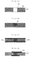
- a through hole 202 is formed in a porous substrate 201 having void 302 and then as illustrated in Fig. 11(b), the through hole 202 is filled with a conductive paste 203 containing a conductive filler and a thermoplastic resin.
- copper foils 204 are overlaid on both side of the porous insulation substrate 201 and the insulation substrate 201 and the copper foils 204 are thermally press-bonded to cure the conductive paste 203 and both copper foils 204 are electrically connected through the conductive paste 203 and as illustrated in Fig. 11(d), the copper foil 204 are patterned in desired patterns to form wiring layers 205.
- the conductive paste 203 is pressurized in the thickness direction and the resin of the conductive paste 203 penetrates the voids 302 of the porous substrate 201. Consequently, the packed density of the conductive particles is increased and the conductive particles are brought into contact with one another to actualize the conductivity and connect wiring layers.
- voids 302 exist in the peripheral parts of the position where the through hole 202 is formed. Attributed to the voids 302, recesses 304 recessed outward in the inner walls of the through hole 202 are formed.
- the conductive paste 203 flows in the recesses 304 and causes so-called paste bleed 305, which is penetration of the insulation substrate layer 201 with the conductive paste.
- the first technique since an electric field tends to be converged upon the paste bleed 305 and electric short circuiting to a wiring layer beside is easily caused attributed to the outward projected shape of the past bleed, the first technique leaves room for improvement in terms of insulation reliability.
- thermosetting resin-containing insulation layer is disposed between an upper and a lower wiring patterns.
- the insulation substrate has a via containing a conductive paste (containing a metal powder, a binder, a solvent and the like).
- the binder and the solvent are removed by heating the insulation substrate. Consequently, gaps are formed among metal powder particles in the via.
- High pressure is applied to the thermosetting resin before complete curing to penetrate the via with the organic resin of the insulation substrate and to fill the gaps among the metal powder particles with the organic resin.
- the loading ratio of the metal powder in the voids in the via is about 65% or higher and the voids are about 35% or lower.
- the voids are entirely filled with the organic resin and the resin is cured.
- the present invention mainly object to provide a wiring substrate with improved reliability of wiring layers in terms of insulation and connection and to provide a method for manufacturing such a wiring substrate.
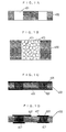
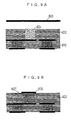
- Fig. 1 to Fig. 5 show the most preferable embodiments of the present invention.
- a via hole 401 is formed in an insulation substrate (an insulation layer) 402.
- the via hole 401 is filled with a conductive paste containing a conductive filler 403 as a functional substance and at the same time at least some of a binder of the conductive paste is removed to form voids 404 in agglomerates of the conductive filler 403 in the via hole 401, that is, the voids 404 are formed in the surroundings of the particles of the conductive filler 403.
- metal foils 405 such as copper foils for forming patterned wirings in both sides are overlaid on both sides and pressurized and laminated and thus the organic resin of the insulation substrate 402 are made to penetrate the foregoing voids 404 to form a via 507.
- the voids 404 in the via 507 are not entirely penetrated with the organic resin of the insulation substrate 402 but some of the voids (first voids) are penetrated with the foregoing organic resin but the remaining voids (second voids) 404' are not penetrated with the foregoing organic resin and positively left as they contain air. In other words, air exists in the second voids 404'.
- a gas other than air may exist in the second voids 404'.
- the conductive filler 403 contains portions where at least conductive filler particles are agglomerated one another.
- the second voids 404' are selectively formed in the agglomerated portions in the conductive filler 403 and the average volume of the second voids 404' is made smaller than the average volume of a plurality of respective conductive filler 403 particles forming at least the agglomerated portions.
- the agglomeration means the situation where second voids are surrounded with a plurality of conductive filler 403 as to leave voids containing air in the inside.
- the metal foils 405 in both sides are processed by a photolithographic method to form wiring layers 407 having desired patterns.
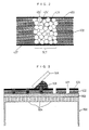
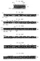
- Fig. 2 shows the situation where the organic resin 406 of the insulation substrate 402 penetrates and exists in some of the first voids 404 in the surroundings of the conductive filler 403 formed by removing at least some of the binder of the conductive paste and also second voids 404' (white depleted parts in Fig. 2) are left as they contain air without being penetrated with the organic resin 406.
- the voids 404 are formed in agglomerates of the conductive filler 403 in the via hole 401 by removing at least some of the binder contained in the conductive paste after the via hole 401 is filled with the conductive paste and the organic resin 406 of the insulation substrate 402 are made to penetrate the voids 404, so that so-called "paste bleed" which is penetration of the insulation substrate 402 with the conductive paste can be avoided.
- the insulation substrate is an insulation resin substrate and contains an organic resin.
- any insulation substrate can be employed without any restriction as long as the insulation substrate is capable of electrically insulating the wiring layers of the wiring substrate one another and besides, is capable of penetrating the organic resin in voids of a via hole. That is, any insulation substrate can be employed if the insulation substrate has a constitution with which an organic resin can be fluidized in the manufacturing process of the wiring substrate.
- Examples with such a constitution include a sheet-like molded material of a thermoplastic resin and/or a thermosetting resin in the semi-cured state as an organic resin; a composite material (prepreg) composed of a thermosetting resin and/or a thermosetting resin in the semi-cured state and organic or inorganic woven or non-woven cloth or a composite material composed of a thermoplastic resin and/or a thermosetting resin in the semi-cured state and an organic or inorganic filler.
- thermoplastic and/or thermosetting resin examples are an epoxy resin, a polyimide resin, a phenol resin, a fluoro resin, an unsaturated polyester resin, a PPE (polyphenylene ether) resin, and a cyanate ester resin.
- organic or inorganic woven or non-woven cloth As the organic or inorganic woven or non-woven cloth, usable ones are woven or non-woven cloths made of organic fibers such as PBO (poly-p-phenylenebenzobisoxazole) fibers, PBI (polybenzoimidazole) fibers, aramide fibers, PTFE (polytetrafluoroethylene) fibers, PBZT (poly-p-phenylenebenzobisthiazole) fibers, and all of aromatic polyester fibers and inorganic fibers such as glass fibers.
- organic or inorganic filler usable substances are aluminum hydroxide, aluminum oxide (alumina), silicon dioxide (silica), and silicon nitride.
- the insulation substrate composed of these materials are an aramide epoxy substrate, a glass epoxy substrate, and the like.
- a conductive filler is not specifically restricted in the shape for use and a powder, a fibrous filler, a granulated body of a powder, a spherical ball, or their mixture can be used.
- the size of the filler may be selected to be suitable to fill a via hole according to the purpose of the present invention. That is, those having a particle size approximately same as the diameter of the via hole can be used.
- the filler may be used while being adjusted as to have a size approximately same as the diameter of the via hole after the granulation.
- the volume ratio of the filler in the via is preferably 30% or higher since filler particles are easily brought into contact with one another to lower the inter-layer connection resistance.
- the conductive fillers are at least one of metals selected from gold, silver, copper, nickel, palladium, lead, tin, indium, and bismuth, their alloys, and their mixture.
- coated fillers composed of balls made of the foregoing metals and alloys and oxides such as alumina and silica and organic synthetic resins and coatings of the foregoing metals and alloys.
- the conductive paste usable ones are those produced by dispersing the foregoing conductive fillers together with, if necessary, an organic resin and/or a binder of a volatile component.
- the organic resin to be used as the binder includes a liquid epoxy resin, a polyimide resin, a cyanate ester resin, a phenol resol resin, and the like.
- the epoxy resin there are glycidyl ether type epoxy resins such as bisphenol A type epoxy resins, bisphenol F type epoxy resins, bisphenol AD type epoxy resins, and the like; alicyclic type epoxy resins; glycidylamine type epoxy resins; epoxy resins having two or more epoxy groups such as glycidyl ester type epoxy resins; and the like.
- any substance can be employed without restrictions if it can be removed by evaporation after filling or during filling and solvents can be used as such a substance.
- solvents can be used as such a substance. Examples are butyl cellosolve, ethyl cellosolve, butylcarbitol, ethylcarbitol, butylcarbitol acetate, ethylcarbitol acetate, and ⁇ -terpineol.
- the binder may contain an additive such as a curing agent for the thermosetting resin and a dispersant for improving the dispersion state of the conductive filler.
- an insulation substrate 402 containing an organic resin and having via holes 401 formed at prescribed positions is made ready.
- Voids may or may not exist in the insulation substrate 402.
- the via holes 401 are formed by a general via hole formation method for a wiring substrate, that is, the mechanical drilling processing, the punching processing, the laser processing using carbon dioxide, excimer, YAG laser, plasma etching, photo-via-processing, and the like.
- via holes of 100 ⁇ m to 250 ⁇ m can be formed by carbon dioxide gas laser of 9.4 ⁇ m to 10.6 ⁇ m wavelength.
- the via holes 401 are filled with a conductive paste from the opening parts in one side of the via hole 401.
- the filling method to be employed is for example a printing method by squeegee 506 illustrated in Fig. 3 and a method for pressure-injection by a dispenser.
- a liquid absorption body 503 is disposed in the opening parts in a manner as illustrated in Fig. 3 on the opposite to the side, in which the conductive paste 508 is injected, so that the absorption body can absorb some of or all of the binder of the conductive paste 508 packed in the via holes 401 simultaneously with or successively to the filling of the via holes 401 with the conductive paste 508 to heighten the loading density (the volume ratio) of the conductive filler 403 as well as to form voids 404 where the binder is expelled in the inside of the via holes 401 as illustrated in Fig. 1(b).
- the binder is sucked in the following conditions until the voids 404 are formed. That is, simultaneously with or after the loading with the conductive paste 508, vacuum suction to 140 to 150 mmHg is carried out. At that time, the voids 404 can be formed in the inside of the via holes 401 in the conditions of 25 to 35 mN/m of the surface tension of the conductive paste 508 (30 to 45 mN/m of the surface tension of the binder resin), 20 [Pa-s] of the viscosity of the conductive paste 508, and 20 to 40 seconds of the suction duration.
- a practical constitution example of the liquid absorption body 503 can be composed, as illustrated in Fig. 3, by mounting an insulation substrate 402 on a vacuum adsorption support 502 and setting the liquid absorption body 503 between them.
- a plurality of holes 504 for suction are formed in the vacuum adsorption support 502 and the conductive paste 508 is packed in the side (the upper face side) opposed to the support 502 and the binder of the conductive paste 508 is sucked to the liquid absorption body 503 to form the voids 404 in which the binder is expelled in the inside of the via holes 401.
- the liquid absorption body 503 substances having a large number of capillary tubes such as sheets of thin paper can be used, and with such a material, the voids 404 can efficiently be formed by the effect of the capillarity of the capillary tubes on the binder besides the binder suction effect of the vacuum adsorption support 502.
- the conductive paste 508 can be prevented from adhering to parts other than the via holes 401.
- metal foils 405 such as copper foils for forming wiring layers 407 having desired patterns are overlaid in both sides and pressurized and laminated.
- the organic resin in the insulation substrate 402 is fluidized and penetrates the voids 404 in the via holes 401. At that time, if necessary, heating is carried out in order to heighten the fluidity of the organic resin or cure the organic resin.
- the pressurizing and laminating process may be carried out for the aramide epoxy substrate with the thickness of 120 ⁇ m in conditions of 50 kgf/cm 2 , 200 °C, for 1 hour while decreasing the ambient pressure to 10 mtorr in case of 100 [Pa-s] of the minimum viscosity of the melt.
- the fluidity of the conductive paste in the via holes 401 is significantly lowered.
- the organic resin from the insulation substrate 402 flows in some of voids 404, that is, the first voids among the voids 404 and the remaining second voids 404' are left as they contain air without being filled with the organic resin.
- the organic resin component enters the first voids and if the binder in the via holes 401 is partially removed, the organic resin and the binder resin of the conductive paste enter the first voids while being mixed each other or in phase separated state (in island state) .
- the conductive filler 403 is in agglomerated state and the second voids 404' are selectively formed in the agglomerated portions of the conductive filler 403.
- the average volume of the second voids 404' is made smaller than the average volume of a plurality of respective conductive filler 403 particles forming at least the agglomerated portions.
- the metal foils 405 in both sides are processed by a conventional method, such as a photolithographic method to form wiring layers 407 having desired patterns and to complete a double-sided wiring substrate illustrated in Fig. 2.
- the conductive filler 403 is agglomerated in the via holes 401 and the organic resin from the insulation substrate 402 enters the first voids and the second voids 404' are selectively left as they are in the portions where the conductive filler 403 exists in agglomerated state.
- the average volume of the second voids 404' is made to be smaller than the average volume of the conductive filler 403.
- the wiring substrate obtained is free from paste bleeding and excellent in insulation reliability.
- voids 404 in the via 507 are filled with the organic resin but the voids 404 are not all filled with the organic resin and the second voids 404' having the smaller average volume than the average volume of the conductive filler are positively left selectively in the agglomerated portions of the conductive filler while containing air, so that the elasticity modulus is lowered and the excellent flexibility is improved.
- the second voids 404' are left selectively in agglomerated portions of the conductive paste having the high elasticity modulus, so that the elasticity modulus in the agglomerated portions where the second voids 404' exist can be lowered.
- One method comprises the process of forming agglomerated portions of the conductive filler and the portions where no agglomeration takes place by incompletely dispersing the conductive filler of the conductive paste and finishing the dispersion while leaving agglomerate to a certain extent at the time when the conductive paste is produced using a dispersing and mixing apparatus.
- the mixture is made to be a paste while keeping the network of the copper powder without completely dissociating the agglomerates of the copper powder particles.
- the other method comprises the process of adding a curing agent for curing a thermosetting resin together with a conductive filler and the thermosetting resin in a conductive paste and using a powder as the curing agent.
- the conductive filler is forced to exist locally in the conductive paste.
- the conductive paste is provided with agglomerated portions of the conductive filler and the portions where no agglomeration takes place.
- the voids can selectively be left in the same manner as described above.
- the conductive filler is not even in the via but exists while being agglomerated to a certain extent. That is a common technique to keep conductivity since if the conductive filler is dispersed too evenly, the contact among conductive filler particles is eliminated to result in deterioration of the conductivity.
- connection reliability can be improved without deteriorating the conductivity by selectively forming the voids in the portions, which are the agglomeration parts of the conductive filler and have the highest elasticity modulus in via, in other words, forming the voids which are in agglomeration parts and hardly penetrated with the organic resin.
- the second voids are surrounded with a plurality of conductive filler particles in agglomerated state where they are firmly connected to each other, the second voids are hardly crushed and left at high ratio and consequently the wiring substrate obtained is provided with a preferable constitution where a low elasticity modulus can be maintained for a long duration, that is, the electric and mechanical connection reliability of the upper and lower wiring layers can be maintained for a long duration.
- any metal foil 405 capable of forming wiring layers 407 can be employed without any particular restriction.
- the metal foil 405 for example, aluminum can be employed.
- a rolled copper foil and an electrolytic copper foil, which are commonly used for wiring substrates, can be used.
- this embodiment is described by employing a method for removing some of the binder of the conductive paste 508 by absorbing it with the liquid absorption body 503 as an example of the process for forming the voids 404 in the via holes 401, there is another method available using a conductive paste 508 containing a volatile component for forming the voids 404 evaporating the volatile component of the conductive paste 508 after the step of filling the via holes 401 with conductive paste 508 or during the step of filling the via holes 401 with conductive paste 508.
- the evaporation of the volatile component can be carried out by a heat drying or vacuum/pressure decrease drying method.
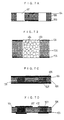
- the formation of the wiring layers 407 is described in this embodiment as to be carried out by overlaying metal foils 405 such as copper foils on both sides and then processing the metal foils 405, there is another method applicable, as illustrated in Fig. 4, which comprises steps of overlaying metal foils 405 in which the wiring layers 407 are previously formed on the insulation substrate 402 in which via holes 401 are so formed as to have voids 404 by removing at least some of the binder of the conductive paste 508 and then pressurizing the metal foils 405.
- the above described method is so-called a transfer method in which metal foils formed on supporting bodies 413 are processed to be wiring layers 407 and being united with the supporting bodies 413, the metal foils are so overlaid on the insulation substrate 402 as to bring the wiring layers 407 into contact with the insulation substrate 402 and then pressurized and then the wiring layers 407 are transferred by removing only the supporting bodies 413 by an etching or mechanically separating method.
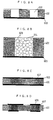
- a four-layer insulation substrate as an example of a multi layer wiring substrate of an embodiment of the present invention can be produced, as illustrated in Fig. 5, by overlaying insulation substrates 402' in which via holes are so formed as to have voids therein by removing at least some of the binder of the conductive paste 508 and further metal foils 412 such as copper foils on the outsides of substrates 402' on both sides of a double-sided wiring substrate as described above [Fig. 1(d) and Fig. 4(b)] or on both sides of a conventionally used both-sided wiring substrate and pressurized and laminated together with the double-sided wiring substrate and then processing the metal foils 412 such as copper foils into wiring layers 407 to obtain the four-layer wiring substrate as illustrated in Fig. 5(b). By repeating such processes, a further multi layer wiring substrate can be obtained.
- insulation substrates In case of using a multi layer substrate, different types of insulation substrates (insulation layers) maybe laminated. For example, using glass-epoxy substrates, one or a plurality of layers of circuits can be formed in one or both sides of a double-sided or multi layer wiring substrate produced from an aramide-epoxy substrate.
- the present invention provides a multi layer wiring substrate possible to mount semiconductor chips of LSI or the like at a high density thereon and suitable to be employed in multi layer structure in which both of a low inter-layer connection resistance and excellent insulation resistance are satisfactorily achieved.
Landscapes
- Engineering & Computer Science (AREA)
- Manufacturing & Machinery (AREA)
- Microelectronics & Electronic Packaging (AREA)
- Production Of Multi-Layered Print Wiring Board (AREA)
- Printing Elements For Providing Electric Connections Between Printed Circuits (AREA)
Abstract
The present invention aims to provide a wiring substrate
highly reliable in insulation and connection and a method for
manufacturing the wiring substrate. The wiring substrate
comprises two or more wiring layers, insulation layers
interposed between the neighboring wiring layers and containing
an organic resin, and via formed in the insulation layers and
extended between neighboring wiring layers. The via contain
functional substances, as well as some of the voids (first
voids) where at least the organic resins from the insulation
layers exist and the remaining voids (second voids) where a gas
exists. Consequently, so-called paste bleed, which is
penetration of an insulation layer with a conductive paste, does
not takes place and the elasticity modulus in the entire via
becomes low and the flexibility is improved attributed to the
second voids in the via. The expansion and the contraction well
respond to the mechanical stress applied to the wiring substrate
and thus disconnected of wiring layers hardly takes place and
the reliability of electric and mechanical connection between
the wiring layers is heightened.
Description
The present invention relates to a wiring substrate and
a manufacturing method thereof, and more particularly, to a
wiring substrate having a low inter-layer connection resistance,
provided with reliability in terms of electric insulation and
reliability in terms of electric and mechanical connection, and
suitable for a multi layer structure and a method for
manufacturing such a wiring substrate.
It is important for a wiring substrate which is so formed
in a multi layer structure as to highly densely mount
semiconductor chips of LSI and the like that a plurality of
wiring layers formed at fine wiring pitches can electrically
be connected to one another at low connection resistance.
For that, in place of a conventional multi layer wiring
substrate employing an inter-layer connection manner by through
holes, a first technique and a second technique for enabling
any electrode of a multi layer wiring substrate to be
inter-layer-connected at any wiring layer position have already
been disclosed in Japanese Unexamined Patent Publication No.
Hei 6 - 268345 and Japanese Unexamined Patent Publication No.
Hei 10 - 335526, respectively.
Hereinafter, the summary of both techniques will be
described.
As it will be described with reference to Fig. 11, the
first technique is to connect only necessary inter-layers by
filling a conductive paste in inner via holes of a multi layer
wiring substrate.
The outline of the connection process will be described
with reference to Fig. 11(a) to Fig. 11(d).
As illustrated in Fig. 11 (a), a through hole 202 is formed
in a porous substrate 201 having void 302 and then as illustrated
in Fig. 11(b), the through hole 202 is filled with a conductive
paste 203 containing a conductive filler and a thermoplastic
resin.
As illustrated in Fig. 11(c), copper foils 204 are
overlaid on both side of the porous insulation substrate 201
and the insulation substrate 201 and the copper foils 204 are
thermally press-bonded to cure the conductive paste 203 and both
copper foils 204 are electrically connected through the
conductive paste 203 and as illustrated in Fig. 11(d), the
copper foil 204 are patterned in desired patterns to form wiring
layers 205.
In the thermal press-bonding process in Fig. 11(c), the
conductive paste 203 is pressurized in the thickness direction
and the resin of the conductive paste 203 penetrates the voids
302 of the porous substrate 201. Consequently, the packed
density of the conductive particles is increased and the
conductive particles are brought into contact with one another
to actualize the conductivity and connect wiring layers.
However, in case of the first technique, since the
insulation substrate 201 is porous, as illustrated in Fig. 12(a),
voids 302 exist in the peripheral parts of the position where
the through hole 202 is formed. Attributed to the voids 302,
recesses 304 recessed outward in the inner walls of the through
hole 202 are formed.
When the through hole 202 having such recesses 304 is
filled with the conductive paste 203 and the copper foils 204
are overlaid and thermally press-bonded, as illustrated in Fig.
12(b), the conductive paste 203 flows in the recesses 304 and
causes so-called paste bleed 305, which is penetration of the
insulation substrate layer 201 with the conductive paste.
In case of the first technique, since an electric field
tends to be converged upon the paste bleed 305 and electric short
circuiting to a wiring layer beside is easily caused attributed
to the outward projected shape of the past bleed, the first
technique leaves room for improvement in terms of insulation
reliability.
In case of the second technique, a thermosetting
resin-containing insulation layer is disposed between an upper
and a lower wiring patterns. The insulation substrate has a
via containing a conductive paste (containing a metal powder,
a binder, a solvent and the like). The binder and the solvent
are removed by heating the insulation substrate. Consequently,
gaps are formed among metal powder particles in the via. High
pressure is applied to the thermosetting resin before complete
curing to penetrate the via with the organic resin of the
insulation substrate and to fill the gaps among the metal powder
particles with the organic resin.
However, in case of the second technique, although there
occurs no so-called paste bleed in which the conductive paste
penetrates the insulation substrate, the loading ratio of the
metal powder in the voids in the via is about 65% or higher and
the voids are about 35% or lower. The voids are entirely filled
with the organic resin and the resin is cured.
For that, no void is left in the entire via and the
elasticity modulus as a whole is increased and the hardness is
high. Therefore, even if mechanical stress is applied to the
wiring substrate by heat in the thickness direction, the entire
body of the wiring substrate is hardly expanded or contracted
responding to the stress and the wiring layers tend to be easily
disconnected with the metal powder in the via. As a result,
there is left room for improvement in terms of the reliability
of electric and mechanical connection between wiring layers.
Consequently, the present invention mainly object to
provide a wiring substrate with improved reliability of wiring
layers in terms of insulation and connection and to provide a
method for manufacturing such a wiring substrate.
Fig. 1 to Fig. 5 show the most preferable embodiments of
the present invention.
A basic manufacture method of a wiring substrate of an
embodiment will be described below
At first, as illustrated in Fig. 1(a), a via hole 401 is
formed in an insulation substrate (an insulation layer) 402.
Next, as illustrated in Fig. 1(b) the via hole 401 is
filled with a conductive paste containing a conductive filler
403 as a functional substance and at the same time at least some
of a binder of the conductive paste is removed to form voids
404 in agglomerates of the conductive filler 403 in the via hole
401, that is, the voids 404 are formed in the surroundings of
the particles of the conductive filler 403.
Then, as illustrated in Fig. 1(c), metal foils 405 such
as copper foils for forming patterned wirings in both sides are
overlaid on both sides and pressurized and laminated and thus
the organic resin of the insulation substrate 402 are made to
penetrate the foregoing voids 404 to form a via 507.
In this case, the voids 404 in the via 507 are not entirely
penetrated with the organic resin of the insulation substrate
402 but some of the voids (first voids) are penetrated with the
foregoing organic resin but the remaining voids (second voids)
404' are not penetrated with the foregoing organic resin and
positively left as they contain air. In other words, air exists
in the second voids 404'.
Incidentally, a gas other than air may exist in the second
voids 404'.
Further, the conductive filler 403 contains portions
where at least conductive filler particles are agglomerated one
another. The second voids 404' are selectively formed in the
agglomerated portions in the conductive filler 403 and the
average volume of the second voids 404' is made smaller than
the average volume of a plurality of respective conductive
filler 403 particles forming at least the agglomerated
portions.
Incidentally, the agglomeration means the situation
where second voids are surrounded with a plurality of conductive
filler 403 as to leave voids containing air in the inside.
Finally, as illustrated in Fig 1 (d), the metal foils 405
in both sides are processed by a photolithographic method to
form wiring layers 407 having desired patterns.
In the above described manner, a double-sided wiring
substrate illustrated in Fig. 2 can be obtained.
Fig. 2 shows the situation where the organic resin 406
of the insulation substrate 402 penetrates and exists in some
of the first voids 404 in the surroundings of the conductive
filler 403 formed by removing at least some of the binder of
the conductive paste and also second voids 404' (white depleted
parts in Fig. 2) are left as they contain air without being
penetrated with the organic resin 406.
In the case of this embodiment, the voids 404 are formed
in agglomerates of the conductive filler 403 in the via hole
401 by removing at least some of the binder contained in the
conductive paste after the via hole 401 is filled with the
conductive paste and the organic resin 406 of the insulation
substrate 402 are made to penetrate the voids 404, so that
so-called "paste bleed" which is penetration of the insulation
substrate 402 with the conductive paste can be avoided.
In the case of this embodiment, if only some of the binder
contained in conductive paste is removed, the situation is
produced where the organic resin component of the insulation
substrate 402 and the binder contained in the conductive paste
exist in the voids 404 while being mixed or being phase-isolated
(island structure).
Hereinafter, a material to be used for the method of
manufacturing the wiring substrate will be described.
The insulation substrate is an insulation resin substrate
and contains an organic resin.
Any insulation substrate can be employed without any
restriction as long as the insulation substrate is capable of
electrically insulating the wiring layers of the wiring
substrate one another and besides, is capable of penetrating
the organic resin in voids of a via hole. That is, any
insulation substrate can be employed if the insulation
substrate has a constitution with which an organic resin can
be fluidized in the manufacturing process of the wiring
substrate.
Examples with such a constitution include a sheet-like
molded material of a thermoplastic resin and/or a thermosetting
resin in the semi-cured state as an organic resin; a composite
material (prepreg) composed of a thermosetting resin and/or a
thermosetting resin in the semi-cured state and organic or
inorganic woven or non-woven cloth or a composite material
composed of a thermoplastic resin and/or a thermosetting resin
in the semi-cured state and an organic or inorganic filler.
As the thermoplastic and/or thermosetting resin, usable
resins are an epoxy resin, a polyimide resin, a phenol resin,
a fluoro resin, an unsaturated polyester resin, a PPE
(polyphenylene ether) resin, and a cyanate ester resin.
As the organic or inorganic woven or non-woven cloth,
usable ones are woven or non-woven cloths made of organic fibers
such as PBO (poly-p-phenylenebenzobisoxazole) fibers, PBI
(polybenzoimidazole) fibers, aramide fibers, PTFE
(polytetrafluoroethylene) fibers, PBZT (poly-p-phenylenebenzobisthiazole)
fibers, and all of aromatic
polyester fibers and inorganic fibers such as glass fibers. As
organic or inorganic filler, usable substances are aluminum
hydroxide, aluminum oxide (alumina), silicon dioxide (silica),
and silicon nitride.
Practical examples of the insulation substrate composed
of these materials are an aramide epoxy substrate, a glass epoxy
substrate, and the like.
A conductive filler is not specifically restricted in the
shape for use and a powder, a fibrous filler, a granulated body
of a powder, a spherical ball, or their mixture can be used.
The size of the filler may be selected to be suitable to fill
a via hole according to the purpose of the present invention.
That is, those having a particle size approximately same as the
diameter of the via hole can be used. Incidentally, in the case
of using the conductive filler while granulating it, the filler
may be used while being adjusted as to have a size approximately
same as the diameter of the via hole after the granulation.
The volume ratio of the filler in the via is preferably
30% or higher since filler particles are easily brought into
contact with one another to lower the inter-layer connection
resistance.
Practical examples of the conductive fillers are at least
one of metals selected from gold, silver, copper, nickel,
palladium, lead, tin, indium, and bismuth, their alloys, and
their mixture. Further, also usable are coated fillers
composed of balls made of the foregoing metals and alloys and
oxides such as alumina and silica and organic synthetic resins
and coatings of the foregoing metals and alloys.
As the conductive paste, usable ones are those produced
by dispersing the foregoing conductive fillers together with,
if necessary, an organic resin and/or a binder of a volatile
component. The organic resin to be used as the binder includes
a liquid epoxy resin, a polyimide resin, a cyanate ester resin,
a phenol resol resin, and the like. As the epoxy resin, there
are glycidyl ether type epoxy resins such as bisphenol A type
epoxy resins, bisphenol F type epoxy resins, bisphenol AD type
epoxy resins, and the like; alicyclic type epoxy resins;
glycidylamine type epoxy resins; epoxy resins having two or more
epoxy groups such as glycidyl ester type epoxy resins; and the
like.
As the volatile component, any substance can be employed
without restrictions if it can be removed by evaporation after
filling or during filling and solvents can be used as such a
substance. Examples are butyl cellosolve, ethyl cellosolve,
butylcarbitol, ethylcarbitol, butylcarbitol acetate,
ethylcarbitol acetate, and α-terpineol.
If necessary, the binder may contain an additive such as
a curing agent for the thermosetting resin and a dispersant for
improving the dispersion state of the conductive filler.
Next, a method for manufacturing the foregoing wiring
substrate will be described in details.
As illustrated in Fig. 1 (a), an insulation substrate 402
containing an organic resin and having via holes 401 formed at
prescribed positions is made ready. Voids may or may not exist
in the insulation substrate 402. The via holes 401 are formed
by a general via hole formation method for a wiring substrate,
that is, the mechanical drilling processing, the punching
processing, the laser processing using carbon dioxide, excimer,
YAG laser, plasma etching, photo-via-processing, and the like.
For example, in case of using an aramide epoxy substrate
of 120 µm thickness, via holes of 100 µm to 250 µm can be formed
by carbon dioxide gas laser of 9.4 µm to 10.6 µm wavelength.
Next, the via holes 401 are filled with a conductive paste
from the opening parts in one side of the via hole 401.
The filling method to be employed is for example a
printing method by squeegee 506 illustrated in Fig. 3 and a
method for pressure-injection by a dispenser.
A liquid absorption body 503 is disposed in the opening
parts in a manner as illustrated in Fig. 3 on the opposite to
the side, in which the conductive paste 508 is injected, so that
the absorption body can absorb some of or all of the binder of
the conductive paste 508 packed in the via holes 401
simultaneously with or successively to the filling of the via
holes 401 with the conductive paste 508 to heighten the loading
density (the volume ratio) of the conductive filler 403 as well
as to form voids 404 where the binder is expelled in the inside
of the via holes 401 as illustrated in Fig. 1(b).
In this case, the binder is sucked in the following
conditions until the voids 404 are formed. That is,
simultaneously with or after the loading with the conductive
paste 508, vacuum suction to 140 to 150 mmHg is carried out.
At that time, the voids 404 can be formed in the inside of the
via holes 401 in the conditions of 25 to 35 mN/m of the surface
tension of the conductive paste 508 (30 to 45 mN/m of the surface
tension of the binder resin), 20 [Pa-s] of the viscosity of the
conductive paste 508, and 20 to 40 seconds of the suction
duration.
However, the conditions are only examples and voids 404
can be formed in other different conditions.
A practical constitution example of the liquid absorption
body 503 can be composed, as illustrated in Fig. 3, by mounting
an insulation substrate 402 on a vacuum adsorption support 502
and setting the liquid absorption body 503 between them.
A plurality of holes 504 for suction are formed in the
vacuum adsorption support 502 and the conductive paste 508 is
packed in the side (the upper face side) opposed to the support
502 and the binder of the conductive paste 508 is sucked to the
liquid absorption body 503 to form the voids 404 in which the
binder is expelled in the inside of the via holes 401.
As the liquid absorption body 503, substances having a
large number of capillary tubes such as sheets of thin paper
can be used, and with such a material, the voids 404 can
efficiently be formed by the effect of the capillarity of the
capillary tubes on the binder besides the binder suction effect
of the vacuum adsorption support 502.
Additionally, if necessary, if a mask 505 is installed
on the insulation substrate 402, the conductive paste 508 can
be prevented from adhering to parts other than the via holes
401.
In the next process, as illustrated in Fig. 1(c), metal
foils 405 such as copper foils for forming wiring layers 407
having desired patterns are overlaid in both sides and
pressurized and laminated.
By the pressure application, the organic resin in the
insulation substrate 402 is fluidized and penetrates the voids
404 in the via holes 401. At that time, if necessary, heating
is carried out in order to heighten the fluidity of the organic
resin or cure the organic resin.
For example, the pressurizing and laminating process may
be carried out for the aramide epoxy substrate with the
thickness of 120 µm in conditions of 50 kgf/cm2, 200 °C, for
1 hour while decreasing the ambient pressure to 10 mtorr in case
of 100 [Pa-s] of the minimum viscosity of the melt.
Since some or all of the binder in the inside of the via
holes 401 is removed to form the voids 404 in the prior process,
the fluidity of the conductive paste in the via holes 401 is
significantly lowered.
As a result, the phenomenon that the conductive paste
flows in the voids 404 even if there exist voids in the insulation
substrate 402, so-called "paste bleed", can be eliminated. On
the other hand, since the fluidity of the organic resin of the
insulation substrate 402 is not changed, the organic resin
penetrates the voids 404 existing in the via holes 401.
In this case, as illustrated in Fig. 2, the organic resin
from the insulation substrate 402 flows in some of voids 404,
that is, the first voids among the voids 404 and the remaining
second voids 404' are left as they contain air without being
filled with the organic resin. Incidentally, if the binder in
the via holes 401 is entirely removed, the organic resin
component enters the first voids and if the binder in the via
holes 401 is partially removed, the organic resin and the binder
resin of the conductive paste enter the first voids while being
mixed each other or in phase separated state (in island state) .
Further, the conductive filler 403 is in agglomerated
state and the second voids 404' are selectively formed in the
agglomerated portions of the conductive filler 403.
The average volume of the second voids 404' is made
smaller than the average volume of a plurality of respective
conductive filler 403 particles forming at least the
agglomerated portions.
Finally, as illustrated in Fig 1(d), the metal foils 405
in both sides are processed by a conventional method, such as
a photolithographic method to form wiring layers 407 having
desired patterns and to complete a double-sided wiring
substrate illustrated in Fig. 2.
In the wiring substrate of this embodiment, as
illustrated in Fig. 2, the conductive filler 403 is agglomerated
in the via holes 401 and the organic resin from the insulation
substrate 402 enters the first voids and the second voids 404'
are selectively left as they are in the portions where the
conductive filler 403 exists in agglomerated state.
Further, the average volume of the second voids 404' is
made to be smaller than the average volume of the conductive
filler 403.
According to this embodiment, the wiring substrate
obtained is free from paste bleeding and excellent in insulation
reliability.
In this case, since the interfaces of the side walls of
via holes are removed, the tensile stress caused in the vias
and the insulation substrate following the bending of the wiring
substrate in the thickness direction and shear stress
attributed to the thermal expansion difference and affecting
the via and the insulation substrate, the separation (break)
of the via holes from the via holes hardly takes place and the
insulation substrate is provided with a firm structure.
Further, in the case where the organic resin in the via holes
and the organic resin of the insulation substrate are the same
material, the structure becomes for firm and the thermal
expansion coefficients of the organic resins are approximately
same to improve the connection reliability.
Further, in this embodiment, only some of voids 404 in
the via 507 are filled with the organic resin but the voids 404
are not all filled with the organic resin and the second voids
404' having the smaller average volume than the average volume
of the conductive filler are positively left selectively in the
agglomerated portions of the conductive filler while containing
air, so that the elasticity modulus is lowered and the excellent
flexibility is improved.
For that, even if the mechanical stress is applied to the
wiring substrate by heat, the expansion and the contraction of
the entire body of the wiring substrate easily follow the stress
and the wiring substrate is provided with high reliability in
the electric and mechanical connection between neighboring
upper and lower patterns.
In this case, although the agglomerated portions of the
conductive filler 403 themselves have a high elasticity modulus,
the second voids 404' are left selectively in agglomerated
portions of the conductive paste having the high elasticity
modulus, so that the elasticity modulus in the agglomerated
portions where the second voids 404' exist can be lowered.
The following two methods, for example, are available to
selectively leave the voids.
One method comprises the process of forming agglomerated
portions of the conductive filler and the portions where no
agglomeration takes place by incompletely dispersing the
conductive filler of the conductive paste and finishing the
dispersion while leaving agglomerate to a certain extent at the
time when the conductive paste is produced using a dispersing
and mixing apparatus.
For example, in case of mixing 87.5 % by weight of a copper
powder of about 5 µm average particle size as a conductive filler
is dispersed in 12.5 % by weight of an epoxy resin by three rolls,
if the gaps among the rolls is controlled to be about 10 µm and
5 passes are performed, the mixture is made to be a paste while
keeping the network of the copper powder without completely
dissociating the agglomerates of the copper powder particles.
Consequently, even during the work of vacuum degassing
and loading the conductive paste, degassing hardly takes place
in the remaining voids surrounded with the agglomerated
portions of the conductive filler and further even in case of
penetrating voids with the organic resin in the process
thereafter, the organic resin hardly penetrates the voids
surrounded with the agglomerated portions of the conductive
filler and easily penetrates the voids which are not surrounded
with the agglomerated portions. As a result, the voids are
selectively left.
The other method comprises the process of adding a curing
agent for curing a thermosetting resin together with a
conductive filler and the thermosetting resin in a conductive
paste and using a powder as the curing agent.
If a powder curing agent having a particle size bigger
than that of the conductive filler is used, the conductive
filler is forced to exist locally in the conductive paste.
Hence, by sucking the resin and the curing agent, the conductive
paste is provided with agglomerated portions of the conductive
filler and the portions where no agglomeration takes place.
Thus, voids surrounded with the agglomeration parts are
hardly penetrated with the organic resin and the voids which
are not surrounded with the agglomeration parts are easily
penetrated with the organic resin. As a result, voids
containing air are selectively left.
Incidentally, even if a conductive powder is used in place
of the conductive paste, the voids can selectively be left in
the same manner as described above.
In this case, the conductive filler is not even in the
via but exists while being agglomerated to a certain extent.
That is a common technique to keep conductivity since if the
conductive filler is dispersed too evenly, the contact among
conductive filler particles is eliminated to result in
deterioration of the conductivity.
For that, the connection reliability can be improved
without deteriorating the conductivity by selectively forming
the voids in the portions, which are the agglomeration parts
of the conductive filler and have the highest elasticity modulus
in via, in other words, forming the voids which are in
agglomeration parts and hardly penetrated with the organic
resin.
Incidentally, in case of positively leaving second voids
having the smaller average volume than the average volume of
respective conductive filler particles, a large amount of the
conductive filler can exist and mechanical and electric
connection of the conductive filler particles are made
excellent.
Further, since the second voids are surrounded with a
plurality of conductive filler particles in agglomerated state
where they are firmly connected to each other, the second voids
are hardly crushed and left at high ratio and consequently the
wiring substrate obtained is provided with a preferable
constitution where a low elasticity modulus can be maintained
for a long duration, that is, the electric and mechanical
connection reliability of the upper and lower wiring layers can
be maintained for a long duration.
Incidentally, although as described above, the manner is
exemplified using a powder curing agent, the same effects can
be obtained by using resin balls, a resin powder, a ceramic
powder and the like with a large particle size than that of the
conductive filler.
Further incidentally, although the description is give
using copper foils as the metal foils 405 for forming wiring
layers 407, any metal foil 405 capable of forming wiring layers
407 can be employed without any particular restriction. As the
metal foil 405, for example, aluminum can be employed. Also
as the copper foil, a rolled copper foil and an electrolytic
copper foil, which are commonly used for wiring substrates, can
be used.
Also, although this embodiment is described by employing
a method for removing some of the binder of the conductive paste
508 by absorbing it with the liquid absorption body 503 as an
example of the process for forming the voids 404 in the via holes
401, there is another method available using a conductive paste
508 containing a volatile component for forming the voids 404
evaporating the volatile component of the conductive paste 508
after the step of filling the via holes 401 with conductive paste
508 or during the step of filling the via holes 401 with
conductive paste 508. The evaporation of the volatile
component can be carried out by a heat drying or vacuum/pressure
decrease drying method.
Although the formation of the wiring layers 407 is
described in this embodiment as to be carried out by overlaying
metal foils 405 such as copper foils on both sides and then
processing the metal foils 405, there is another method
applicable, as illustrated in Fig. 4, which comprises steps of
overlaying metal foils 405 in which the wiring layers 407 are
previously formed on the insulation substrate 402 in which via
holes 401 are so formed as to have voids 404 by removing at least
some of the binder of the conductive paste 508 and then
pressurizing the metal foils 405.
More particularly, the above described method is so-called
a transfer method in which metal foils formed on
supporting bodies 413 are processed to be wiring layers 407 and
being united with the supporting bodies 413, the metal foils
are so overlaid on the insulation substrate 402 as to bring the
wiring layers 407 into contact with the insulation substrate
402 and then pressurized and then the wiring layers 407 are
transferred by removing only the supporting bodies 413 by an
etching or mechanically separating method.
A four-layer insulation substrate as an example of a multi
layer wiring substrate of an embodiment of the present invention
can be produced, as illustrated in Fig. 5, by overlaying
insulation substrates 402' in which via holes are so formed as
to have voids therein by removing at least some of the binder
of the conductive paste 508 and further metal foils 412 such
as copper foils on the outsides of substrates 402' on both sides
of a double-sided wiring substrate as described above [Fig. 1(d)
and Fig. 4(b)] or on both sides of a conventionally used
both-sided wiring substrate and pressurized and laminated
together with the double-sided wiring substrate and then
processing the metal foils 412 such as copper foils into wiring
layers 407 to obtain the four-layer wiring substrate as
illustrated in Fig. 5(b). By repeating such processes, a
further multi layer wiring substrate can be obtained.
Incidentally, although the description is given as an
example of a method of manufacturing the foregoing multi layer
wiring substrate by using insulation substrates 402' in both
sides of the double-sided wiring substrate, it is possible to
use a multi layer wiring substrate having 2 or more layers in
place of the double-sided substrate.
In case of using a multi layer substrate, different types
of insulation substrates (insulation layers) maybe laminated.
For example, using glass-epoxy substrates, one or a plurality
of layers of circuits can be formed in one or both sides of a
double-sided or multi layer wiring substrate produced from an
aramide-epoxy substrate.
The present invention provides a multi layer wiring
substrate possible to mount semiconductor chips of LSI or the
like at a high density thereon and suitable to be employed in
multi layer structure in which both of a low inter-layer
connection resistance and excellent insulation resistance are
satisfactorily achieved.
Claims (25)
- A wiring substrate comprising:two or more wiring layers;insulation layers interposed between said neighboring wiring layers and containing an organic resin; andvia formed in the insulation layers as to connect said wiring layers one another,wherein said via is characterized in containing a plurality of functional substances while keeping voids in the surroundings, andwherein the voids include first voids where at least the organic resins from the insulation layers exist and second voids where a gas exists.
- The wiring substrate as claimed in claim 1, characterized in that said second voids are selectively formed in the portions where the agglomerated functional substances exist.
- The wiring substrate as claimed in claim 2, characterized in that said second voids have a smaller average volume than the average volume of a plurality of the respective functional substances forming at least the agglomeration portions among the functional substances.
- The wiring substrate as claimed in claim 1, characterized in that said functional substances are one or more conductive fillers, and
that said insulation layers are made of composite materials of organic or inorganic woven cloth impregnated with said organic resins or composite materials of organic or inorganic non-woven cloth impregnated with the organic resins. - The wiring substrate as claimed in claim 1, characterized in that said functional substances are one or more conductive fillers, and
that said insulation layers are made of composite materials containing organic or inorganic fillers and said organic resins. - A wiring substrate comprising:two or more wiring layers;insulation layers interposed between said neighboring wiring layers; andvia formed in the insulation layers as to connect said wiring layers one another,wherein said insulation layers comprise films and adhesive layers containing adhesives and formed at least one side, andwherein said via contain functional substances and the adhesives of said adhesive layers penetrating and existing in the voids in the surroundings of the functional substances.
- The wiring substrate as claimed in claim 6, characterized in that said voids include first voids where at least said adhesive exist and second voids where a gas exists.
- The wiring substrate as claimed in claim 7, characterized in that said functional substances are agglomerated and said second voids are selectively formed in the portions where the agglomerated functional substances exist, among said functional substances.
- The wiring substrate as claimed in claim 8, characterized in that said second voids have a smaller average volume than the average volume of a plurality of the respective functional substances forming at least the agglomeration portions among the functional substances.
- The wiring substrate as claimed in claim 8, characterized in that the volume ratio of said functional substances occupying said via is 30% or higher.
- A method for manufacturing a wiring substrate comprising:a first process of forming via in which voids are formed by filling functional substances in via holes formed in an insulation substrate containing an organic resin and removing at least some of the functional substances; anda second process of making said voids be first voids in which at least an organic resin from the insulation substrate exists and be second voids in which a gas exists.
- The method for manufacturing a wiring substrate as claimed in claim 11, characterized in that said functional substances are agglomerated and said second voids are selectively formed in the portions where said agglomerated functional substances exist in said second process.
- The method for manufacturing a wiring substrate as claimed in claim 11, characterized in that the average volume of said second voids is made smaller than the average volume of a plurality of the respective functional substances forming at least the agglomeration portions in said second process.
- A method for manufacturing a wiring substrate comprising:a first process of forming via in which voids are formed by filling functional substances in via holes formed in an insulation substrate of a film bearing an adhesive layer containing adhesives in at least one side; anda second process of penetrating the voids of said via hole with the adhesive of said adhesive layer.
- The method for manufacturing a wiring substrate as claimed in claim 14, characterized in that said voids are selectively penetrated with said adhesive in said second process.
- The method for manufacturing a wiring substrate as claimed in claim 15, characterized in that first voids are penetrated with the adhesive by being selectively penetrated with said adhesive by agglomerating said functional substances and second voids where a gas exist are formed in said second process.
- The method for manufacturing a wiring substrate as claimed in claim 16, characterized in that the average volume of said second voids is made smaller than the average volume of a plurality of the respective functional substances forming at least the agglomeration portions in said second process.
- The method for manufacturing a wiring substrate as claimed in claim 11, characterized in that said first process is carried out using one or more conductive fillers as said functional substances and comprises a step of filling said via holes with a conductive paste containing the conductive fillers and an organic binder and a step of removing at least a part of the organic binder of said conductive paste.
- The method for manufacturing a wiring substrate as claimed in claim 18, characterized in that said organic binder contains a volatile component and at least a part of said organic binder is removed by evaporating said volatile component.
- The method for manufacturing a wiring substrate as claimed in claim 18, characterized in that at least a part of said organic binder is removed by sucking said organic binder.
- The method for manufacturing a wiring substrate as claimed in claim 11, characterized in that said first process is carried out using one or more conductive fillers as the functional substances and comprises a step of filling said via holes with the conductive fillers.
- The method for manufacturing a wiring substrate as claimed in claim 21, characterized in that said conductive fillers are granulated bodies produced by granulating conductive particles.
- The method for manufacturing a wiring substrate as claimed in claim 11, characterized in that the first voids are penetrated with the organic resin by applying pressure to an insulation substrate in the thickness direction by metal conductors disposed in both sides of the insulation substrate.
- The method for manufacturing a wiring substrate as claimed in claim 14, characterized in that the voids in via are penetrated with the adhesive by applying pressure to an insulation substrate in the thickness direction by metal conductors disposed in both sides of the insulation substrate.
- The method for manufacturing a wiring substrate as claimed in either claim 11 or claim 14, characterized in that said metal conductors are either metal foils or wiring patterns.
Applications Claiming Priority (3)
| Application Number | Priority Date | Filing Date | Title |
|---|---|---|---|
| JP33575899 | 1999-11-26 | ||
| JP33575899 | 1999-11-26 | ||
| PCT/JP2000/008274 WO2001039561A1 (en) | 1999-11-26 | 2000-11-24 | Wiring board and production method thereof |
Publications (2)
| Publication Number | Publication Date |
|---|---|
| EP1156707A1 true EP1156707A1 (en) | 2001-11-21 |
| EP1156707A4 EP1156707A4 (en) | 2006-12-20 |
Family
ID=18292141
Family Applications (1)
| Application Number | Title | Priority Date | Filing Date |
|---|---|---|---|
| EP00977895A Withdrawn EP1156707A4 (en) | 1999-11-26 | 2000-11-24 | PCB and its production |
Country Status (4)
| Country | Link |
|---|---|
| US (1) | US6774316B1 (en) |
| EP (1) | EP1156707A4 (en) |
| TW (1) | TW498707B (en) |
| WO (1) | WO2001039561A1 (en) |
Cited By (1)
| Publication number | Priority date | Publication date | Assignee | Title |
|---|---|---|---|---|
| IT201700100522A1 (en) * | 2017-09-07 | 2019-03-07 | Technoprobe Spa | Interface element for an electronic device test device and its manufacturing method |
Families Citing this family (39)
| Publication number | Priority date | Publication date | Assignee | Title |
|---|---|---|---|---|
| JPWO2003009656A1 (en) | 2001-07-18 | 2004-11-11 | 松下電器産業株式会社 | Circuit forming substrate manufacturing method and circuit forming substrate |
| JP4951832B2 (en) * | 2001-08-31 | 2012-06-13 | 凸版印刷株式会社 | Method for producing transparent conductive film |
| JP4062907B2 (en) * | 2001-11-12 | 2008-03-19 | 松下電器産業株式会社 | Circuit board and manufacturing method thereof |
| US6826830B2 (en) * | 2002-02-05 | 2004-12-07 | International Business Machines Corporation | Multi-layered interconnect structure using liquid crystalline polymer dielectric |
| WO2004019668A1 (en) * | 2002-08-21 | 2004-03-04 | Hoya Corporation | Perforated substrate, method for manufacturing same and full wafer contact board |
| CN100359659C (en) * | 2003-02-18 | 2008-01-02 | Jsr株式会社 | Anisotropic conductive connector, probing member and wafer inspection device, and wafer inspection method |
| US20050014035A1 (en) * | 2003-07-16 | 2005-01-20 | Matsushita Electric Industrial Co., Ltd. | Prepreg for printed wiring board, printed wiring board using the prepreg and method for manufacturing the printed wiring board, and multilayer printed wiring board and method for manufacturing the multilayer printed wiring board |
| US7488895B2 (en) * | 2003-09-29 | 2009-02-10 | Panasonic Corporation | Method for manufacturing component built-in module, and component built-in module |
| TW200611612A (en) | 2004-09-29 | 2006-04-01 | Unimicron Technology Corp | Process of electrically interconnect structure |
| JP4764688B2 (en) * | 2004-10-22 | 2011-09-07 | 日本無線株式会社 | Triplate type planar slot antenna |
| JP4747707B2 (en) * | 2004-11-09 | 2011-08-17 | ソニー株式会社 | Multilayer wiring board and board manufacturing method |
| US7334323B2 (en) * | 2005-07-11 | 2008-02-26 | Endicott Interconnect Technologies, Inc. | Method of making mutilayered circuitized substrate assembly having sintered paste connections |
| US7514116B2 (en) * | 2005-12-30 | 2009-04-07 | Intel Corporation | Horizontal Carbon Nanotubes by Vertical Growth and Rolling |
| EP1890524A4 (en) * | 2006-04-03 | 2009-07-01 | Panasonic Corp | MULTILAYER PRINTED WIRING BOARD AND METHOD FOR MANUFACTURING THE SAME |
| CN101573784B (en) * | 2006-12-18 | 2013-01-09 | 松下电器产业株式会社 | Electrode structure and bump forming method |
| JP2007189257A (en) * | 2007-04-09 | 2007-07-26 | Matsushita Electric Ind Co Ltd | Circuit board manufacturing material |
| US20080311738A1 (en) * | 2007-06-18 | 2008-12-18 | Lakshmi Supriya | Method of forming an interconnect joint |
| JP2009049136A (en) * | 2007-08-17 | 2009-03-05 | Fujitsu Ltd | Wiring board, wiring pattern forming method, and wiring board manufacturing method |
| JP2009300801A (en) * | 2008-06-13 | 2009-12-24 | Sony Corp | Optical package, manufacturing method thereof, backlight, and liquid crystal display device |
| JP4713682B1 (en) * | 2010-02-25 | 2011-06-29 | パナソニック株式会社 | Multilayer wiring board and method for manufacturing multilayer wiring board |
| JP4616927B1 (en) * | 2010-02-25 | 2011-01-19 | パナソニック株式会社 | WIRING BOARD, WIRING BOARD MANUFACTURING METHOD, AND VIA PASTE |
| JP2011193290A (en) * | 2010-03-15 | 2011-09-29 | Seiko Instruments Inc | Method of manufacturing package, piezoelectric vibrator, oscillator, electronic apparatus, and radio-controlled timepiece |
| CN103052501B (en) * | 2010-07-30 | 2015-08-26 | 京瓷株式会社 | Insulating trip, its manufacture method and have employed the manufacture method of structure of this insulating trip |
| JP4859999B1 (en) * | 2010-12-21 | 2012-01-25 | パナソニック株式会社 | Multilayer wiring substrate, multilayer wiring substrate manufacturing method, and via paste |
| JP4917668B1 (en) * | 2010-12-29 | 2012-04-18 | パナソニック株式会社 | Multilayer wiring board and method for manufacturing multilayer wiring board |
| JP4795488B1 (en) * | 2011-01-18 | 2011-10-19 | パナソニック株式会社 | WIRING BOARD, WIRING BOARD MANUFACTURING METHOD, AND VIA PASTE |
| US8723049B2 (en) * | 2011-06-09 | 2014-05-13 | Tessera, Inc. | Low-stress TSV design using conductive particles |
| JP5099272B1 (en) * | 2011-12-26 | 2012-12-19 | パナソニック株式会社 | Multilayer wiring board and manufacturing method thereof |
| TW201340807A (en) * | 2011-12-28 | 2013-10-01 | 松下電器產業股份有限公司 | Flexible wiring board, method for manufacturing flexible wiring board, package product using flexible wiring board, and flexible multilayer wiring board |
| CN103314652A (en) * | 2012-01-17 | 2013-09-18 | 松下电器产业株式会社 | Wiring substrate and production method therefor |
| DE102012201976A1 (en) * | 2012-02-10 | 2013-08-14 | Robert Bosch Gmbh | Component with a via |
| WO2014046014A1 (en) * | 2012-09-20 | 2014-03-27 | 株式会社クラレ | Circuit board and method for manufacturing same |
| TWI477209B (en) * | 2014-04-08 | 2015-03-11 | Azotek Co Ltd | Composite substrate |
| JP6361464B2 (en) * | 2014-10-24 | 2018-07-25 | 富士通株式会社 | Wiring structure |
| KR101953962B1 (en) * | 2017-01-09 | 2019-03-04 | 서울대학교산학협력단 | Forming method of stretchable substrate having via and stretchable substrate having via |
| US11600421B2 (en) * | 2017-04-14 | 2023-03-07 | The Diller Corporation | Laminate with induction coils |
| US11605487B2 (en) * | 2017-04-14 | 2023-03-14 | The Diller Corporation | Laminate with induction coils and charging station device comprising same |
| KR102454686B1 (en) * | 2020-12-30 | 2022-10-13 | 에스케이씨 주식회사 | Surface treated copper foil and circuit board including the same |
| JP7582509B2 (en) * | 2021-11-18 | 2024-11-13 | 株式会社村田製作所 | Wiring Board |
Family Cites Families (9)
| Publication number | Priority date | Publication date | Assignee | Title |
|---|---|---|---|---|
| US5624741A (en) * | 1990-05-31 | 1997-04-29 | E. I. Du Pont De Nemours And Company | Interconnect structure having electrical conduction paths formable therein |
| US5614043A (en) * | 1992-09-17 | 1997-03-25 | Coors Ceramics Company | Method for fabricating electronic components incorporating ceramic-metal composites |
| CN1044762C (en) * | 1993-09-22 | 1999-08-18 | 松下电器产业株式会社 | Printed circuit board and manufacturing method thereof |
| US5435480A (en) * | 1993-12-23 | 1995-07-25 | International Business Machines Corporation | Method for filling plated through holes |
| JPH09116273A (en) | 1995-08-11 | 1997-05-02 | Shinko Electric Ind Co Ltd | Multilayer circuit board and method of manufacturing the same |
| US6103359A (en) * | 1996-05-22 | 2000-08-15 | Jsr Corporation | Process and apparatus for manufacturing an anisotropic conductor sheet and a magnetic mold piece for the same |
| US6143116A (en) * | 1996-09-26 | 2000-11-07 | Kyocera Corporation | Process for producing a multi-layer wiring board |
| JP3112258B2 (en) * | 1997-05-30 | 2000-11-27 | 京セラ株式会社 | Circuit board and its manufacturing method |
| JPH11145176A (en) * | 1997-11-11 | 1999-05-28 | Fujitsu Ltd | Solder bump forming method and preliminary solder forming method |
-
2000
- 2000-11-23 TW TW089124870A patent/TW498707B/en not_active IP Right Cessation
- 2000-11-24 WO PCT/JP2000/008274 patent/WO2001039561A1/en not_active Ceased
- 2000-11-24 US US09/890,145 patent/US6774316B1/en not_active Expired - Fee Related
- 2000-11-24 EP EP00977895A patent/EP1156707A4/en not_active Withdrawn
Cited By (3)
| Publication number | Priority date | Publication date | Assignee | Title |
|---|---|---|---|---|
| IT201700100522A1 (en) * | 2017-09-07 | 2019-03-07 | Technoprobe Spa | Interface element for an electronic device test device and its manufacturing method |
| WO2019048299A1 (en) * | 2017-09-07 | 2019-03-14 | Technoprobe S.P.A. | Interface element for a testing apparatus of electronic devices and corresponding manufacturing method |
| US11293941B2 (en) | 2017-09-07 | 2022-04-05 | Technoprobe S.P.A. | Interface element for a testing apparatus of electronic devices and corresponding manufacturing method |
Also Published As
| Publication number | Publication date |
|---|---|
| EP1156707A4 (en) | 2006-12-20 |
| US6774316B1 (en) | 2004-08-10 |
| WO2001039561A1 (en) | 2001-05-31 |
| TW498707B (en) | 2002-08-11 |
Similar Documents
| Publication | Publication Date | Title |
|---|---|---|
| US6774316B1 (en) | Wiring board and production method thereof | |
| US7103971B2 (en) | Process for manufacturing a circuit board | |
| US6855892B2 (en) | Insulation sheet, multi-layer wiring substrate and production processes thereof | |
| US6799369B2 (en) | Printed circuit board and method for producing the same | |
| US5888627A (en) | Printed circuit board and method for the manufacture of same | |
| US20020045394A1 (en) | Wiring board and a process of producing a wiring board | |
| EP0645951B1 (en) | Printed circuit board and method of manufacturing the same | |
| JP2002290051A (en) | Component built-in module and manufacturing method thereof | |
| WO2004066316A1 (en) | Conductive paste, method for producing same, circuit board using such conductive paste and method for producing same | |
| JP3014365B2 (en) | Wiring board, intermediate connector, method of manufacturing wiring board, and method of manufacturing intermediate connector | |
| US20030137815A1 (en) | Printed wiring board and method of manufacturing the same | |
| CN1229002C (en) | Circuit formed substrate and method of manufacturing circuit formed substrate | |
| US7059044B2 (en) | Method and material for manufacturing circuit-formed substrate | |
| EP1353541A1 (en) | Circuit board and production method therefor | |
| JP5439165B2 (en) | Multilayer wiring board and manufacturing method thereof | |
| JPH1117295A (en) | Method of manufacturing prepreg for circuit board, prepreg for circuit board, and method of manufacturing circuit board using prepreg for circuit board | |
| JP4175824B2 (en) | Multilayer wiring board and method and apparatus for manufacturing the same | |
| JPH10335834A (en) | Multilayer wiring board | |
| JP3238901B2 (en) | Multilayer printed wiring board and method of manufacturing the same | |
| JP2002329967A (en) | Manufacturing method of multilayer printed wiring board | |
| JP2003017855A (en) | Manufacturing method of multilayer printed-wiring board | |
| JP2008181915A (en) | Multilayer printed wiring board and manufacturing method thereof | |
| JPWO2001039561A1 (en) | Wiring board and manufacturing method thereof | |
| JP2002176268A (en) | Resin substrate, method of manufacturing resin substrate, connection intermediate, circuit board, and method of manufacturing circuit board | |
| JP2007142147A (en) | Conductive paste composition, printed wiring board using the same, and method for producing the same |
Legal Events
| Date | Code | Title | Description |
|---|---|---|---|
| PUAI | Public reference made under article 153(3) epc to a published international application that has entered the european phase |
Free format text: ORIGINAL CODE: 0009012 |
|
| 17P | Request for examination filed |
Effective date: 20010727 |
|
| AK | Designated contracting states |
Kind code of ref document: A1 Designated state(s): AT BE CH CY DE DK ES FI FR GB GR IE IT LI LU MC NL PT SE TR |
|
| AX | Request for extension of the european patent |
Free format text: AL;LT;LV;MK;RO;SI |
|
| RBV | Designated contracting states (corrected) |
Designated state(s): DE FR GB |
|
| A4 | Supplementary search report drawn up and despatched |
Effective date: 20061116 |
|
| STAA | Information on the status of an ep patent application or granted ep patent |
Free format text: STATUS: THE APPLICATION IS DEEMED TO BE WITHDRAWN |
|
| 18D | Application deemed to be withdrawn |
Effective date: 20070216 |