EP1156528A1 - Electric connection structure for electronic power devices and method of connection - Google Patents
Electric connection structure for electronic power devices and method of connection Download PDFInfo
- Publication number
- EP1156528A1 EP1156528A1 EP00830337A EP00830337A EP1156528A1 EP 1156528 A1 EP1156528 A1 EP 1156528A1 EP 00830337 A EP00830337 A EP 00830337A EP 00830337 A EP00830337 A EP 00830337A EP 1156528 A1 EP1156528 A1 EP 1156528A1
- Authority
- EP
- European Patent Office
- Prior art keywords
- semiconductor material
- region
- face
- material body
- peripheral region
- Prior art date
- Legal status (The legal status is an assumption and is not a legal conclusion. Google has not performed a legal analysis and makes no representation as to the accuracy of the status listed.)
- Granted
Links
Images

Classifications
-
- H—ELECTRICITY
- H10—SEMICONDUCTOR DEVICES; ELECTRIC SOLID-STATE DEVICES NOT OTHERWISE PROVIDED FOR
- H10W—GENERIC PACKAGES, INTERCONNECTIONS, CONNECTORS OR OTHER CONSTRUCTIONAL DETAILS OF DEVICES COVERED BY CLASS H10
- H10W42/00—Arrangements for protection of devices
-
- H—ELECTRICITY
- H10—SEMICONDUCTOR DEVICES; ELECTRIC SOLID-STATE DEVICES NOT OTHERWISE PROVIDED FOR
- H10W—GENERIC PACKAGES, INTERCONNECTIONS, CONNECTORS OR OTHER CONSTRUCTIONAL DETAILS OF DEVICES COVERED BY CLASS H10
- H10W72/00—Interconnections or connectors in packages
- H10W72/01—Manufacture or treatment
- H10W72/015—Manufacture or treatment of bond wires
- H10W72/01515—Forming coatings
-
- H—ELECTRICITY
- H10—SEMICONDUCTOR DEVICES; ELECTRIC SOLID-STATE DEVICES NOT OTHERWISE PROVIDED FOR
- H10W—GENERIC PACKAGES, INTERCONNECTIONS, CONNECTORS OR OTHER CONSTRUCTIONAL DETAILS OF DEVICES COVERED BY CLASS H10
- H10W72/00—Interconnections or connectors in packages
- H10W72/071—Connecting or disconnecting
- H10W72/075—Connecting or disconnecting of bond wires
-
- H—ELECTRICITY
- H10—SEMICONDUCTOR DEVICES; ELECTRIC SOLID-STATE DEVICES NOT OTHERWISE PROVIDED FOR
- H10W—GENERIC PACKAGES, INTERCONNECTIONS, CONNECTORS OR OTHER CONSTRUCTIONAL DETAILS OF DEVICES COVERED BY CLASS H10
- H10W72/00—Interconnections or connectors in packages
- H10W72/50—Bond wires
- H10W72/531—Shapes of wire connectors
- H10W72/536—Shapes of wire connectors the connected ends being ball-shaped
-
- H—ELECTRICITY
- H10—SEMICONDUCTOR DEVICES; ELECTRIC SOLID-STATE DEVICES NOT OTHERWISE PROVIDED FOR
- H10W—GENERIC PACKAGES, INTERCONNECTIONS, CONNECTORS OR OTHER CONSTRUCTIONAL DETAILS OF DEVICES COVERED BY CLASS H10
- H10W72/00—Interconnections or connectors in packages
- H10W72/50—Bond wires
- H10W72/531—Shapes of wire connectors
- H10W72/5363—Shapes of wire connectors the connected ends being wedge-shaped
-
- H—ELECTRICITY
- H10—SEMICONDUCTOR DEVICES; ELECTRIC SOLID-STATE DEVICES NOT OTHERWISE PROVIDED FOR
- H10W—GENERIC PACKAGES, INTERCONNECTIONS, CONNECTORS OR OTHER CONSTRUCTIONAL DETAILS OF DEVICES COVERED BY CLASS H10
- H10W72/00—Interconnections or connectors in packages
- H10W72/50—Bond wires
- H10W72/59—Bond pads specially adapted therefor
-
- H—ELECTRICITY
- H10—SEMICONDUCTOR DEVICES; ELECTRIC SOLID-STATE DEVICES NOT OTHERWISE PROVIDED FOR
- H10W—GENERIC PACKAGES, INTERCONNECTIONS, CONNECTORS OR OTHER CONSTRUCTIONAL DETAILS OF DEVICES COVERED BY CLASS H10
- H10W72/00—Interconnections or connectors in packages
- H10W72/90—Bond pads, in general
-
- H—ELECTRICITY
- H10—SEMICONDUCTOR DEVICES; ELECTRIC SOLID-STATE DEVICES NOT OTHERWISE PROVIDED FOR
- H10W—GENERIC PACKAGES, INTERCONNECTIONS, CONNECTORS OR OTHER CONSTRUCTIONAL DETAILS OF DEVICES COVERED BY CLASS H10
- H10W72/00—Interconnections or connectors in packages
- H10W72/90—Bond pads, in general
- H10W72/951—Materials of bond pads
-
- H—ELECTRICITY
- H10—SEMICONDUCTOR DEVICES; ELECTRIC SOLID-STATE DEVICES NOT OTHERWISE PROVIDED FOR
- H10W—GENERIC PACKAGES, INTERCONNECTIONS, CONNECTORS OR OTHER CONSTRUCTIONAL DETAILS OF DEVICES COVERED BY CLASS H10
- H10W72/00—Interconnections or connectors in packages
- H10W72/90—Bond pads, in general
- H10W72/951—Materials of bond pads
- H10W72/952—Materials of bond pads comprising metals or metalloids, e.g. PbSn, Ag or Cu
-
- H—ELECTRICITY
- H10—SEMICONDUCTOR DEVICES; ELECTRIC SOLID-STATE DEVICES NOT OTHERWISE PROVIDED FOR
- H10W—GENERIC PACKAGES, INTERCONNECTIONS, CONNECTORS OR OTHER CONSTRUCTIONAL DETAILS OF DEVICES COVERED BY CLASS H10
- H10W90/00—Package configurations
- H10W90/701—Package configurations characterised by the relative positions of pads or connectors relative to package parts
- H10W90/751—Package configurations characterised by the relative positions of pads or connectors relative to package parts of bond wires
- H10W90/756—Package configurations characterised by the relative positions of pads or connectors relative to package parts of bond wires between a chip and a stacked lead frame, conducting package substrate or heat sink
Definitions
- the present invention regards an electric connection structure for electronic power devices, and a method of connection.
- elementary cells comprising BJT NPN or MOS transistors with a high integration level so as to be inserted in ever smaller packages.
- the self-aligned double-polysilicon technology is widely used, which enables cut-off frequencies higher than 50 GHz to be reached.
- the individual transistors are insulated by trenches filled with insulating material, so as to reduce the parasitic capacitance towards the substrate and to reduce the size of the BJT device, or through diffused regions around the active area.
- the emitter, base and collector contacts are generally provided on the front of the wafer, at pads, and are connected to the pins of the device by wire bonding.
- the support region in order to prevent excessive bending of the connection wire (or connection wires if a multiple connection is required), the support region must have a peripheral portion (around the die) of considerable dimensions.
- the support region at present it is required for the support region to have a free wire-soldering area having a width (i.e., distance between the edge of the die and the edge of the support region) of at least 300 ⁇ m for each side on which a connection wire is to be bonded.
- the aim of the present invention is therefore to provide an electric connection structure that solves the problems of known solutions.
- an electronic device and a relative method of connection are provided, as defined in claim 1 and claim 6, respectively.
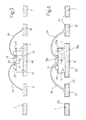
- Figures 1 and 2 show a portion of a sheet tape 1 (hereinafter referred to as "reel"), on which a die 2 is already bonded, the die being designed to house a power device of the bottom-collector, bottom-base, bottom-emitter, bottom-drain, bottom-source, or bottom-gate type.
- the die 2 houses a bipolar gain transistor 3 (represented with its equivalent electric circuit in Figure 2), of the high-frequency, high-power, and bottom-emitter type.
- the reel 1 defines a plurality of blanks 5 identical to the one shown in Figure 1, one for each die 2, the geometry of which (after the electric connection, the formation of an encapsulation package, and cutting of the reel 1) is designed to form a support region for the die, as well as electrodes or pins.
- the blank 5 of Figure 1 comprises a support region 10, arranged at the center, and four electrodes 11, 12, 13, 14 laterally delimited by empty areas 9.
- two electrodes 11, 12, arranged diagonally opposite to one another with respect to the support region 10 are separate from the support region 10 and from one another, and are joined to the reel 1 only at external portions of the blank 5.
- the electrodes 13, 14, which also extend diagonally opposite to one another from the support region 10, are connected to the support region 10, and are hence at the same potential.
- the electrode 11 is intended to be connected to a collector region
- the electrode 12 is intended to be connected to a base region
- the electrodes 13, 14 are intended to be connected to the emitter region, which is in turn appropriately biased, for example grounded.
- the die 2 comprises a body 15 of P + -type semiconductor material, integrating the bipolar gain transistor 3.
- the body 15 has a first face 15a fixed to the support region 10, a second face 15b opposite to the first face, and a side surface 15c.
- the body 15 has low resistivity, for instance 10-20 m ⁇ /cm.
- a passivation layer 16 extends over the second face 15b of the body 15.
- the passivation layer 16 is open at two pads 20, 21, which are electrically connected, in a known way that is not illustrated, respectively to the base region and collector region of the bipolar gain transistor 3.
- the passivation layer 16 is removed at the front outer perimeter of the die 2 and leaves uncovered a metal strip 22 which extends directly on the second face 15b of the body 15 or is anyway electrically connected to the body 15.
- the method of connection comprises initially forming the metal strip 22 and the pads 20, 21, preferably simultaneously.
- the die 2 is bonded on the support region 10, according to known techniques, and the pads 20, 21 are electrically connected to the respective electrodes 11, 12, through connection wires 24, in a known way (wire-bonding step).
- the structure shown in Figure 3 is thus obtained.
- a conductive layer 25 of metallic material grows isotropically.
- the metallic material is preferably chosen from among the group comprising gold, copper, lead, tin, and nickel, or is a lead-tin alloy.
- the thickness of the conductive layer 25 depends upon the application requirements (typically upon the current flowing and the impedance desired at the envisaged operating frequency) and may, for instance, be 10 ⁇ m.
- the conductive layer 25 grows on the whole reel 1, so as to coat the electrodes 11-14 (only the electrodes 11, 12 may be seen in Figure 4), on the connection wires 24, which become thicker, around the support region 10 (where the latter is uncovered), on the side surface 15c of the body 15, and on the metal strip 22.
- a portion 25a of the conductive layer 25 electrically connects the metal strip 22, and thus the emitter region of the bipolar gain transistor 3, to the support region 10, thus electrically connecting the emitter region to the potential of the surface 15a of the body 15.
- This connection is possible thanks to the low conductivity of the body 15, whose side surface 15c is also covered by the growing portion 25a of the conductive layer 25. The structure shown in Figure 4 is thus obtained.
- the base region and collector region of the bipolar gain transistor 3 are connected to their respective electrodes 11, 12 in a standard way, via the connection wires 24, and the emitter region is connected to ground and to the electrodes 13, 14 via the portion 25a of the conductive layer 25.
- connection system In the first place, the electronic device has a much smaller size than known devices with equal performance. In fact, the area necessary on the top side of the die 2 for forming the pads is reduced, considering that, for wires having a diameter of 25.6 ⁇ m a soldering area of 60x60 ⁇ m 2 is required, and that two adjacent connection wires must be positioned at least 150 ⁇ m apart for avoiding mutual inductance.
- the support region 10 does not have to be sized so as to enable soldering of the wires, but can be chosen to be just slightly larger than the die 2.
- the portion 25a of the conductive layer 25 represents a considerable metallic mass that is able to carry a high current (the metallic mass of the portion 25a is proportional to the size of the die 2, as well as to the thickness of the conductive layer 25; consequently, with a 10 ⁇ m thick conductive layer 25, a 50.6- ⁇ m section of side surface 15c of the body 15 is equivalent to a wire having a diameter of 25.6 ⁇ m).
- connection wires 24 are thus obtained having a diameter such as ones normally requiring much larger pads.
- the growth of the conductive layer 25 is carried out simultaneously for all the blanks 5 of a reel 1, thus obtaining simultaneous connection between all the metal strips 22 and their respective support regions 10 and dispensing with numerous soldering operations for separate connection by through one or more wires.
- connection structure and to the electrical method of connection described and illustrated herein, all falling within the scope of the invention, as defined in the attached claims.
- present method is applicable to all devices having a terminal connected to the bottom area of the body 15, including integrated, as well as discrete, circuits.
- the metal strip 22 may also be discontinuous and not extend over the entire periphery of the die 2, when it is not necessary to exploit the entire lateral surface of the die 2 for the connection.
Landscapes
- Wire Bonding (AREA)
Abstract
Description
- Figure 1 is a top view of a die bonded to a blank; and
- Figures 2-4 are cross sections of the blank and of the die of Figure 1, taken along cross-section line II-II, in subsequent manufacture steps.
Claims (11)
- An electronic device (3) formed in a semiconductor material body (15) fixed to a support body (10) of conductive material and having a first terminal, characterized by a peripheral region (22) of conductive material connected to said first terminal and extending on at least one peripheral portion of said body of semiconductor material (15), and a connection region (25a) extending on said peripheral region (22) and surrounding at least partially said semiconductor material body (15) and said support body (10).
- The device of claim 1, characterized in that said semiconductor material body (15) has a first face (15a) fixed to said support body (10) and a second face (15b) opposite to said first face, and in that said peripheral region (22) extends on the periphery of said second face (15b).
- The device of claim 2, characterized in that said peripheral region (22) extends along the entire periphery of said second face (15b), and said connection region (25a) extends completely on a lateral surface (15c) of said semiconductor material body (15).
- The device according to any of the foregoing claims, characterized in that said peripheral region (22) and said connection region (25a) are made of a metallic material.
- The device according to any of the foregoing claims, characterized in that it comprises a second terminal connected to a respective electrode (11, 12) via a pad (20, 21) and a conductive wire (24), and in that at least one metal region (25) surrounds said electrode (11, 12), said conductive wire (24) and said pad (20, 21).
- The device of claim 5, characterized in that said peripheral region (22), said connection region (25a), and said metallic region (25) are made of a metal chosen from among a group comprising gold, copper, lead, tin, and nickel and a lead-tin alloy.
- A method for connecting a semiconductor material body (15) to a reel (1), said semiconductor material body housing an electronic device (3) having a first terminal, and said reel (1) comprising a blank (5) forming a support body (10) and a first electrode (13, 14), the method comprising the step of fixing said semiconductor material body (15) to said support body (10), characterized by the steps of:before fixing said semiconductor material body (15) to said support body (10), forming a peripheral region (22) of conductive material connected to said first terminal and extending over at least one peripheral portion of said semiconductor material body (15); andafter said step of fixing, forming a connection region (25a) extending over said peripheral region (22) and surrounding at least partially said semiconductor material body (15) and said support body (10).
- The method of claim 7, characterized in that, simultaneously with said peripheral region (22), the step is carried out of forming, on said semiconductor material body (15), at least one pad (20, 21) insulated from said semiconductor material body and electrically connected to a second terminal of said electronic device (3), and in that, prior to said step of fixing, the step is carried out of fixing at least one conductive wire (24) between said pad (20, 21) and said first electrode (11, 12).
- The method of claim 7 or claim 8, characterized in that said semiconductor material body (15) has a first face (15a) fixed to said support body (10) and a second face (15b) opposite to said first face, and in that said peripheral region (22) extends over the entire periphery of said second face (15b).
- The method of claim 9, characterized in that said peripheral region (22) extends along the entire periphery of said second face (15b), and said connection region (25a) extends completely on a lateral surface (15c) of said semiconductor material body (15).
- The method according to any of claims 7-10, characterized in that said step of forming a connection region (25a) is carried out by galvanic growth of metallic material on said reel (1).
Priority Applications (3)
| Application Number | Priority Date | Filing Date | Title |
|---|---|---|---|
| EP00830337A EP1156528B1 (en) | 2000-05-08 | 2000-05-08 | Electric connection structure for electronic power devices and method of connection |
| DE60030417T DE60030417D1 (en) | 2000-05-08 | 2000-05-08 | Electrical connection structure for electronic power devices and connection method |
| US09/850,724 US6627982B2 (en) | 2000-05-08 | 2001-05-07 | Electric connection structure for electronic power devices, and method of connection |
Applications Claiming Priority (1)
| Application Number | Priority Date | Filing Date | Title |
|---|---|---|---|
| EP00830337A EP1156528B1 (en) | 2000-05-08 | 2000-05-08 | Electric connection structure for electronic power devices and method of connection |
Publications (2)
| Publication Number | Publication Date |
|---|---|
| EP1156528A1 true EP1156528A1 (en) | 2001-11-21 |
| EP1156528B1 EP1156528B1 (en) | 2006-08-30 |
Family
ID=8175320
Family Applications (1)
| Application Number | Title | Priority Date | Filing Date |
|---|---|---|---|
| EP00830337A Expired - Lifetime EP1156528B1 (en) | 2000-05-08 | 2000-05-08 | Electric connection structure for electronic power devices and method of connection |
Country Status (3)
| Country | Link |
|---|---|
| US (1) | US6627982B2 (en) |
| EP (1) | EP1156528B1 (en) |
| DE (1) | DE60030417D1 (en) |
Cited By (1)
| Publication number | Priority date | Publication date | Assignee | Title |
|---|---|---|---|---|
| DE10204403A1 (en) * | 2002-02-04 | 2003-08-21 | Infineon Technologies Ag | Device for connecting an IC connection to a reference potential |
Families Citing this family (5)
| Publication number | Priority date | Publication date | Assignee | Title |
|---|---|---|---|---|
| US20160277017A1 (en) * | 2011-09-13 | 2016-09-22 | Fsp Technology Inc. | Snubber circuit |
| US8941962B2 (en) * | 2011-09-13 | 2015-01-27 | Fsp Technology Inc. | Snubber circuit and method of using bipolar junction transistor in snubber circuit |
| WO2016150583A1 (en) * | 2015-03-24 | 2016-09-29 | Abb Technology Ag | Power semiconductor device and power semiconductor module comprising a power semiconductor device |
| US20200098698A1 (en) * | 2018-09-26 | 2020-03-26 | Intel Corporation | Novel wafer level chip scale package (wlcsp), flip-chip chip scale package (fccsp), and fan out shielding concepts |
| IT202300011052A1 (en) * | 2023-05-31 | 2024-12-01 | St Microelectronics Int Nv | Digital temperature sensor, corresponding device and procedure |
Citations (6)
| Publication number | Priority date | Publication date | Assignee | Title |
|---|---|---|---|---|
| DE3337796A1 (en) * | 1983-10-18 | 1985-04-25 | Metz Apparatewerke Inh. Paul Metz, 8510 Fürth | Integrated device |
| US4839717A (en) * | 1986-12-19 | 1989-06-13 | Fairchild Semiconductor Corporation | Ceramic package for high frequency semiconductor devices |
| GB2244376A (en) * | 1990-05-24 | 1991-11-27 | Mitsubishi Electric Corp | A semiconductor device |
| US5371411A (en) * | 1980-09-01 | 1994-12-06 | Hitachi, Ltd. | Resin molded type semiconductor device having a conductor film |
| US6032356A (en) * | 1993-11-16 | 2000-03-07 | Formfactor. Inc. | Wafer-level test and burn-in, and semiconductor process |
| US6046507A (en) * | 1997-12-08 | 2000-04-04 | Advanced Micro Devices | Electrophoretic coating methodology to improve internal package delamination and wire bond reliability |
Family Cites Families (11)
| Publication number | Priority date | Publication date | Assignee | Title |
|---|---|---|---|---|
| US5365108A (en) * | 1992-11-19 | 1994-11-15 | Sundstrand Corporation | Metal matrix composite semiconductor power switch assembly |
| JP3275536B2 (en) * | 1994-05-31 | 2002-04-15 | 三菱電機株式会社 | Semiconductor device and manufacturing method thereof |
| JP3269745B2 (en) * | 1995-01-17 | 2002-04-02 | 株式会社日立製作所 | Modular semiconductor device |
| JP3168901B2 (en) * | 1996-02-22 | 2001-05-21 | 株式会社日立製作所 | Power semiconductor module |
| CN1146988C (en) * | 1997-12-08 | 2004-04-21 | 东芝株式会社 | Package for semiconductor power device and method for assembling the same |
| US6396127B1 (en) * | 1998-09-25 | 2002-05-28 | International Rectifier Corporation | Semiconductor package |
| US6127716A (en) * | 1998-10-09 | 2000-10-03 | Kabushiki Kaisha Toshiba | Heterojunction bipolar transistor and manufacturing method thereof |
| DE19953594A1 (en) * | 1998-11-20 | 2000-05-25 | Matsushita Electric Industrial Co Ltd | Surface-mounted electronic component, e.g. a capacitor, has electrodes of migration resistant material formed on the entire surface of a substrate |
| JP4037589B2 (en) * | 2000-03-07 | 2008-01-23 | 三菱電機株式会社 | Resin-encapsulated power semiconductor device |
| JP2001308264A (en) * | 2000-04-21 | 2001-11-02 | Toyota Industries Corp | Semiconductor device |
| JP3830726B2 (en) * | 2000-04-26 | 2006-10-11 | 松下電器産業株式会社 | Thermally conductive substrate, manufacturing method thereof, and power module |
-
2000
- 2000-05-08 EP EP00830337A patent/EP1156528B1/en not_active Expired - Lifetime
- 2000-05-08 DE DE60030417T patent/DE60030417D1/en not_active Expired - Lifetime
-
2001
- 2001-05-07 US US09/850,724 patent/US6627982B2/en not_active Expired - Lifetime
Patent Citations (6)
| Publication number | Priority date | Publication date | Assignee | Title |
|---|---|---|---|---|
| US5371411A (en) * | 1980-09-01 | 1994-12-06 | Hitachi, Ltd. | Resin molded type semiconductor device having a conductor film |
| DE3337796A1 (en) * | 1983-10-18 | 1985-04-25 | Metz Apparatewerke Inh. Paul Metz, 8510 Fürth | Integrated device |
| US4839717A (en) * | 1986-12-19 | 1989-06-13 | Fairchild Semiconductor Corporation | Ceramic package for high frequency semiconductor devices |
| GB2244376A (en) * | 1990-05-24 | 1991-11-27 | Mitsubishi Electric Corp | A semiconductor device |
| US6032356A (en) * | 1993-11-16 | 2000-03-07 | Formfactor. Inc. | Wafer-level test and burn-in, and semiconductor process |
| US6046507A (en) * | 1997-12-08 | 2000-04-04 | Advanced Micro Devices | Electrophoretic coating methodology to improve internal package delamination and wire bond reliability |
Cited By (2)
| Publication number | Priority date | Publication date | Assignee | Title |
|---|---|---|---|---|
| DE10204403A1 (en) * | 2002-02-04 | 2003-08-21 | Infineon Technologies Ag | Device for connecting an IC connection to a reference potential |
| US7057271B2 (en) | 2002-02-04 | 2006-06-06 | Infineon Technologies Ag | Apparatus for connecting an IC terminal to a reference potential |
Also Published As
| Publication number | Publication date |
|---|---|
| US20020070432A1 (en) | 2002-06-13 |
| US6627982B2 (en) | 2003-09-30 |
| EP1156528B1 (en) | 2006-08-30 |
| DE60030417D1 (en) | 2006-10-12 |
Similar Documents
| Publication | Publication Date | Title |
|---|---|---|
| US8076755B2 (en) | Semiconductor device and method of manufacturing the same | |
| US8294208B2 (en) | Semiconductor device having a gate contact on one surface electrically connected to a gate bus on an opposing surface | |
| TWI401800B (en) | Real wafer level package power metal oxide semiconductor field effect transistor based on bottom-source metal oxide semiconductor field effect transistor and manufacturing method thereof | |
| US6177707B1 (en) | Semiconductor device comprising a glass supporting body onto which a substrate with semiconductor elements and a metalization is attached by means of an adhesive | |
| JP2006278646A (en) | Manufacturing method of semiconductor device | |
| US20050205986A1 (en) | Module with integrated active substrate and passive substrate | |
| JP2006505955A (en) | Chip scale Schottky device | |
| JP5154000B2 (en) | Semiconductor device | |
| US6689642B2 (en) | Semiconductor device and manufacturing method thereof | |
| EP1156528B1 (en) | Electric connection structure for electronic power devices and method of connection | |
| US6127716A (en) | Heterojunction bipolar transistor and manufacturing method thereof | |
| US6953981B1 (en) | Semiconductor device with deep substrates contacts | |
| US5888889A (en) | Integrated structure pad assembly for lead bonding | |
| US6897547B2 (en) | Semiconductor device including bipolar junction transistor, and production method therefor | |
| US5569952A (en) | Semiconductor device with a semiconductor element provided in a mesa structure | |
| EP0415106B1 (en) | Lead frames for semiconductor device | |
| US6188123B1 (en) | Semiconductor element having vertical discrete bipolar transistor and semiconductor device having same | |
| US7375397B2 (en) | Semiconductor device having an SOI structure and method for manufacturing the same | |
| US4984051A (en) | Semiconductor device having directly connected source terminal | |
| EP0450320A1 (en) | Semiconductor integrated circuit device for high frequency signal processing | |
| EP4310906A1 (en) | Semiconductor package and method | |
| JP2003069015A (en) | Semiconductor device | |
| JP2000311976A (en) | High frequency bipolar transistor | |
| EP3955289A1 (en) | Four terminal transistor package | |
| JP2005033154A (en) | Semiconductor device |
Legal Events
| Date | Code | Title | Description |
|---|---|---|---|
| PUAI | Public reference made under article 153(3) epc to a published international application that has entered the european phase |
Free format text: ORIGINAL CODE: 0009012 |
|
| AK | Designated contracting states |
Kind code of ref document: A1 Designated state(s): AT BE CH CY DE DK ES FI FR GB GR IE IT LI LU MC NL PT SE Kind code of ref document: A1 Designated state(s): DE FR GB IT |
|
| AX | Request for extension of the european patent |
Free format text: AL;LT;LV;MK;RO;SI |
|
| 17P | Request for examination filed |
Effective date: 20020515 |
|
| AKX | Designation fees paid |
Free format text: DE FR GB IT |
|
| 17Q | First examination report despatched |
Effective date: 20050520 |
|
| GRAP | Despatch of communication of intention to grant a patent |
Free format text: ORIGINAL CODE: EPIDOSNIGR1 |
|
| GRAS | Grant fee paid |
Free format text: ORIGINAL CODE: EPIDOSNIGR3 |
|
| GRAA | (expected) grant |
Free format text: ORIGINAL CODE: 0009210 |
|
| AK | Designated contracting states |
Kind code of ref document: B1 Designated state(s): DE FR GB IT |
|
| PG25 | Lapsed in a contracting state [announced via postgrant information from national office to epo] |
Ref country code: IT Free format text: LAPSE BECAUSE OF FAILURE TO SUBMIT A TRANSLATION OF THE DESCRIPTION OR TO PAY THE FEE WITHIN THE PRESCRIBED TIME-LIMIT;WARNING: LAPSES OF ITALIAN PATENTS WITH EFFECTIVE DATE BEFORE 2007 MAY HAVE OCCURRED AT ANY TIME BEFORE 2007. THE CORRECT EFFECTIVE DATE MAY BE DIFFERENT FROM THE ONE RECORDED. Effective date: 20060830 |
|
| REG | Reference to a national code |
Ref country code: GB Ref legal event code: FG4D |
|
| REF | Corresponds to: |
Ref document number: 60030417 Country of ref document: DE Date of ref document: 20061012 Kind code of ref document: P |
|
| PG25 | Lapsed in a contracting state [announced via postgrant information from national office to epo] |
Ref country code: DE Free format text: LAPSE BECAUSE OF FAILURE TO SUBMIT A TRANSLATION OF THE DESCRIPTION OR TO PAY THE FEE WITHIN THE PRESCRIBED TIME-LIMIT Effective date: 20061201 |
|
| ET | Fr: translation filed | ||
| PLBE | No opposition filed within time limit |
Free format text: ORIGINAL CODE: 0009261 |
|
| STAA | Information on the status of an ep patent application or granted ep patent |
Free format text: STATUS: NO OPPOSITION FILED WITHIN TIME LIMIT |
|
| 26N | No opposition filed |
Effective date: 20070531 |
|
| PGFP | Annual fee paid to national office [announced via postgrant information from national office to epo] |
Ref country code: IT Payment date: 20070524 Year of fee payment: 8 |
|
| GBPC | Gb: european patent ceased through non-payment of renewal fee |
Effective date: 20070508 |
|
| PGFP | Annual fee paid to national office [announced via postgrant information from national office to epo] |
Ref country code: FR Payment date: 20070529 Year of fee payment: 8 |
|
| PG25 | Lapsed in a contracting state [announced via postgrant information from national office to epo] |
Ref country code: GB Free format text: LAPSE BECAUSE OF NON-PAYMENT OF DUE FEES Effective date: 20070508 |
|
| REG | Reference to a national code |
Ref country code: FR Ref legal event code: ST Effective date: 20090119 |
|
| PG25 | Lapsed in a contracting state [announced via postgrant information from national office to epo] |
Ref country code: FR Free format text: LAPSE BECAUSE OF NON-PAYMENT OF DUE FEES Effective date: 20080602 |
|
| PG25 | Lapsed in a contracting state [announced via postgrant information from national office to epo] |
Ref country code: IT Free format text: LAPSE BECAUSE OF NON-PAYMENT OF DUE FEES Effective date: 20080508 |