EP1156524A1 - Manufacturing process of an integrated circuit including high-density and logic components portion - Google Patents
Manufacturing process of an integrated circuit including high-density and logic components portion Download PDFInfo
- Publication number
- EP1156524A1 EP1156524A1 EP00201716A EP00201716A EP1156524A1 EP 1156524 A1 EP1156524 A1 EP 1156524A1 EP 00201716 A EP00201716 A EP 00201716A EP 00201716 A EP00201716 A EP 00201716A EP 1156524 A1 EP1156524 A1 EP 1156524A1
- Authority
- EP
- European Patent Office
- Prior art keywords
- polysilicon layer
- integrated circuit
- layer
- circuit components
- performance logic
- Prior art date
- Legal status (The legal status is an assumption and is not a legal conclusion. Google has not performed a legal analysis and makes no representation as to the accuracy of the status listed.)
- Granted
Links
- 238000004519 manufacturing process Methods 0.000 title description 10
- 229910021420 polycrystalline silicon Inorganic materials 0.000 claims abstract description 89
- 229920005591 polysilicon Polymers 0.000 claims abstract description 89
- 238000000034 method Methods 0.000 claims abstract description 40
- 239000004065 semiconductor Substances 0.000 claims abstract description 22
- 229910021332 silicide Inorganic materials 0.000 claims abstract description 15
- FVBUAEGBCNSCDD-UHFFFAOYSA-N silicide(4-) Chemical compound [Si-4] FVBUAEGBCNSCDD-UHFFFAOYSA-N 0.000 claims abstract description 14
- 239000000758 substrate Substances 0.000 claims abstract description 13
- 230000010354 integration Effects 0.000 claims abstract description 11
- 230000015654 memory Effects 0.000 claims description 63
- 239000002184 metal Substances 0.000 claims description 23
- 239000002019 doping agent Substances 0.000 claims description 9
- 125000006850 spacer group Chemical group 0.000 claims description 6
- 238000007669 thermal treatment Methods 0.000 claims description 6
- 238000000151 deposition Methods 0.000 claims description 5
- XUIMIQQOPSSXEZ-UHFFFAOYSA-N Silicon Chemical group [Si] XUIMIQQOPSSXEZ-UHFFFAOYSA-N 0.000 claims description 4
- 150000004767 nitrides Chemical class 0.000 claims description 4
- 239000011810 insulating material Substances 0.000 claims description 2
- 230000015572 biosynthetic process Effects 0.000 description 7
- 239000011159 matrix material Substances 0.000 description 6
- 230000008021 deposition Effects 0.000 description 3
- 238000005530 etching Methods 0.000 description 2
- 238000000059 patterning Methods 0.000 description 2
- 229920002120 photoresistant polymer Polymers 0.000 description 2
- 229910008814 WSi2 Inorganic materials 0.000 description 1
- 238000003491 array Methods 0.000 description 1
- 230000000295 complement effect Effects 0.000 description 1
- 238000005516 engineering process Methods 0.000 description 1
- 230000006870 function Effects 0.000 description 1
- 239000007943 implant Substances 0.000 description 1
- 238000002513 implantation Methods 0.000 description 1
- 230000000873 masking effect Effects 0.000 description 1
- 230000004048 modification Effects 0.000 description 1
- 238000012986 modification Methods 0.000 description 1
- 238000002310 reflectometry Methods 0.000 description 1
- 229910052710 silicon Inorganic materials 0.000 description 1
- 239000010703 silicon Substances 0.000 description 1
Images





Classifications
-
- H—ELECTRICITY
- H10—SEMICONDUCTOR DEVICES; ELECTRIC SOLID-STATE DEVICES NOT OTHERWISE PROVIDED FOR
- H10B—ELECTRONIC MEMORY DEVICES
- H10B41/00—Electrically erasable-and-programmable ROM [EEPROM] devices comprising floating gates
- H10B41/40—Electrically erasable-and-programmable ROM [EEPROM] devices comprising floating gates characterised by the peripheral circuit region
-
- H—ELECTRICITY
- H10—SEMICONDUCTOR DEVICES; ELECTRIC SOLID-STATE DEVICES NOT OTHERWISE PROVIDED FOR
- H10B—ELECTRONIC MEMORY DEVICES
- H10B41/00—Electrically erasable-and-programmable ROM [EEPROM] devices comprising floating gates
-
- H—ELECTRICITY
- H10—SEMICONDUCTOR DEVICES; ELECTRIC SOLID-STATE DEVICES NOT OTHERWISE PROVIDED FOR
- H10B—ELECTRONIC MEMORY DEVICES
- H10B41/00—Electrically erasable-and-programmable ROM [EEPROM] devices comprising floating gates
- H10B41/40—Electrically erasable-and-programmable ROM [EEPROM] devices comprising floating gates characterised by the peripheral circuit region
- H10B41/42—Simultaneous manufacture of periphery and memory cells
- H10B41/49—Simultaneous manufacture of periphery and memory cells comprising different types of peripheral transistor
Definitions
- the present invention relates generally to the field of integrated circuit technology, and more specifically to the manufacturing of high-density integrated circuits, typically semiconductor memories, particularly but not exclusively non-volatile ones, and logic circuits. Still more specifically, the invention relates to a manufacturing process for the integration in same chip of a high-density integrated circuit portion, typically a memory, and high-performance logic integrated circuit portion.
- the most of the chip area is occupied by the array of memory cells, the so-called memory matrix.
- the dimensions of the memory cells have to be shrunk, so as to pack more and more memory cells per chip unit area.
- the reason why the contact dimensions cannot be easily shrunk is mainly lithographic, and gives rise to an increased defectivity, that is, a low production yield.
- SAC Self-Aligned Contact
- high-performance logic circuits take advantage of another technique, known as salicidation, or self-aligned silicidation, providing for a self-aligned formation of metal silicides on active areas and on polysilicon layers.
- salicidation or self-aligned silicidation
- metal silicides on active areas and on polysilicon layers.
- the use of salicidation has made possible higher circuit performance.
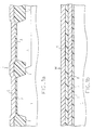
- Figures 1A and 1B schematically show in cross-section a first portion L and, respectively, a second portion M of a semiconductor chip in which high-performance logic circuits and a semiconductor memory will be integrated.
- the first portion L of the chip will host a pair of complementary transistors of a high-performance logic circuit
- the second portion M will host a pair of memory cells of a memory cell matrix for a semiconductor memory, particularly a non-volatile memory such as an EPROM, an EEPROM or a Flash EEPROM.
- field oxide regions 2 are selectively formed in any conventional way, e.g. by means of the so-called LOCOS technique. Between the field oxide regions 2, a logic transistor gate oxide layer 3 is formed over a surface of the substrate 1. The thickness of the logic transistor gate oxide layer 3 is for example in the range 20-100 ⁇ . From the logic transistor gate oxide layer 3, gate oxides of the transistors of the high-performance logic circuit will be formed.
- N type wells 4 are formed in the P type substrate 1.
- N-channel transistors of the high-performance logic circuit can be formed directly in the P type substrate 1 or, if preferred, P type wells with suitable doping can be formed in the P type substrate 1. It is to be noted that the conductivity type of the substrate 1, and thus that of the well 4, can be opposite to those previously described.
- a polysilicon layer 5 is deposited over the field oxide regions 2 and the gate oxide layer 3.
- a memory cell gate oxide layer 6 is formed over the substrate 1 .
- the oxide layer 6 can be the logic transistor gate oxide layer 3 or a different oxide layer, depending on the type of memory cells which are to be formed (EPROM, EEPROM, Flash EEPROM).
- the thickness of the memory cell gate oxide layer 6 is for example in the range 70-120 ⁇ .
- a polysilicon layer 7 is deposited.
- the polysilicon layer 7 is a first, lower polysilicon layer (first poly), while the polysilicon layer 5 previously mentioned is a second, upper polysilicon layer (second poly) .
- the first polysilicon layer 7 will be used to form floating gates of the memory cells.
- a dielectric layer 8 is formed over the first polysilicon layer 7.
- the interpoly dielectric is formed as a triple layer comprised of a lower oxide layer, an intermediate nitride layer, and an upper oxide layer (Oxide-Nitride-Oxide or ONO).
- the second polysilicon layer 5 will form the control gates of the memory cells.
- the second polysilicon layer 5 is then submitted to selective doping to reduce the resistivity thereof.
- the portions of the polysilicon layer 5 which will have to form the gates of N-channel transistors are doped with N type dopants, while the portions of the polysilicon layer 5 that will have to form the gates of the P-channel transistors are doped with P type dopants.
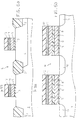
- a first mask is used to expose the portions of the polysilicon layer 5 that, after definition, will form the gates of N-channel transistors of the high-performance logic circuit, protecting from dopant implantation at least the portions of polysilicon layer 5 which will form the gates of the P-channel transistors of the high-performance logic circuit; the same mask 9 can also leave exposed the portions of the polysilicon layer 5 which will form the control gates of the memory cells.
- a suitable N type dopant such as As or P in a dose of 5*10 14 to 5*10 15 , is then implanted into the exposed portions of the polysilicon layer 5, that is the portions from which the gates of the N-channel transistors of the high-performance logic circuit will be formed, and optionally the portions from which the control gates of the memory cells will be formed.
- a second mask indicated as 10 in Figure 3
- a suitable P type dopant such as B or BF 2 in a dose of 5*10 14 to 5*10 15 , is then implanted into the exposed portions of the polysilicon layer 5. Then, also the second mask 10 is removed.
- a metal silicide layer 11, e.g. WSi 2 is then formed over the polysilicon layer 5 to further increase the conductivity thereof.
- a layer of a suitable metal, such as W is first deposited over the polysilicon layer 5; then, by means of a suitable thermal treatment, the metal atoms are made to react with the silicon atoms in the polysilicon layer 5 so as to form the silicide layer 11.
- the silicide layer 11, also called polycide, is formed over the whole of the polysilicon layer 5, that is both over the portions of the polysilicon layer 5 that will form the gates of the N-channel and P-channel transistors of the high-performance logic circuit ( Figure 4A), and over the portions of the polysilicon layer 5 which will form the control gates of the memory cells ( Figure 4B). It is worth remarking that the polysilicon layer 5 is silicidated before the patterning thereof.
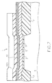
- a dielectric layer 12 such as a nitride layer is formed over the silicide layer 11, typically by deposition.
- a dielectric layer 12 will be used to form a so-called hard mask for the definition (patterning) of the polysilicon layer 5.
- Provision of a hard mask is advantageous in the definition of sub-micrometric geometries in polysilicon layers, thanks to the fact that it increases the degree of reflectivity of the structure to be defined.
- a photoresist layer is deposited over the chip, then by means of a photolithographic mask the photoresist layer is selectively exposed to light, it is developed to selectively remove it, and then a selective etch is carried out.
- the dielectric layer 12 is selectively removed, thus forming a hard mask that leaves exposed the portions of the polysilicon layer 5 which will have to be removed in the following steps.
- a resist mask 120 covers all the chip surface, except from regions of the dielectric layer 12 which are to be removed to allow access to the underlying polysilicon layer 5; preferably, such regions are located over the field oxide 2.
- the dielectric layer 12 is then etched away from the exposed regions, so as to expose the surface of the polysilicon layer 5.
- the following process steps provide for the formation, in conventional ways, of source regions and drain regions 13 and 14 for the N-channel and, respectively, P-channel transistors of the high-performance logic circuit.
- the source and drain regions 13 and 14 of the transistors of the high-performance logic circuit have the so-called Lightly-Doped Drain (LDD) structure, with a shallower, relatively lightly doped portion 131, 141 aside the gate structures, and a deeper, more heavily doped portion 132, 142 farther from the gate structures.
- LDD Lightly-Doped Drain
- Such a structure is obtained by firstly introducing into the substrate, in self alignment with the gate structures of the transistors, a relatively light dose of dopants, then forming insulating material sidewall spacers 17 at the sides of the gate structures, extending down to the substrate surface so as to cover the lightly doped portions 131, 141 of the source and drain regions 13, 14, and then forming the deeper, more heavily doped portions 132, 142 of the source and drain regions. Sidewall spacers 17 are also inherently formed at the sides of the gate structures of the memory cells.
- Salicidation of the active areas is also contemplated: to this end, a layer of a suitable metal such as Ti or Co is firstly deposited over the whole surface of the chip, then a thermal treatment is carried out; during the thermal treatment, the metal atoms react with silicon atoms to form a metal silicide; this only takes place where the metal atoms lies directly over silicon or polysilicon, while over the dielectric layers and the sidewall spacers no reaction takes place and no silicide is formed.
- a suitable metal such as Ti or Co
- the polysilicon layer 5 has previously been submitted to a blank silicidation and a polycide layer 11 has been formed over the polysilicon layer 5.
- the electric performance of the polycide layer 11 are substantially equivalent to those of a salicide layer.
- the formation of salicide regions 18 where contacts to the polysilicon layer 5 are to be formed improves the contact conductivity.
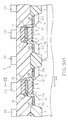
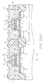
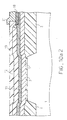
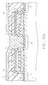
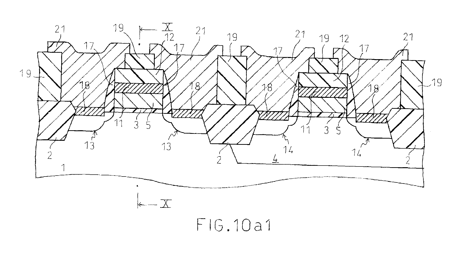
- FIGS 9A1, 9A2 which is a cross-section along line IX-IX in Figure 9A1) and 9B
- the structure is ready to receive by deposition a dielectric layer 19, in which contact openings will formed.
- a mask 20 contact mask
- the openings in the contact mask 20 extend over the gate structures of the memory cells, and possibly also over the gate structures of the transistors of the high-performance logic circuit.
- the contact openings to be opened in the dielectric layer are defined in self-alignment with the gate structures of the memory cells and, possibly, also of the transistors of the high-performance logic circuit.
- this is not a concern, since during the following selective etch to remove the dielectric layer 19, such gate structures are not damaged, due to the presence of the hard mask layer 12 and the sidewall spacers 17 that protect the polysilicon layer 5.
- a metal layer 21 is deposited over the chip; the metal layer 21 penetrates into the contact openings thus contacting, through the respective salicide regions 18, the source and drain regions 13, 14 and the gate of the transistors of the high performance logic circuit, and the drain regions 16 of the memory cells. Similar contacts to the source regions 15 of the memory cells, not shown, will clearly be provided for in selected regions of the memory matrix.
- the metal layer 21 is then patterned to define metal strips.
- the process according to the present invention is suitable for the integration in a same chip of a high-performance logic circuit and a memory, particularly a non-volatile one.
- the process according to the invention allows to take advantage of the techniques of salicidation of active areas, from one hand, and Self-Aligned Contact (SAC) formation from the other hand: the first technique allows to increase the performance of logic circuits, by reducing the resistivity of the source and drain regions of the transistors, while the second technique allows to form compact arrays of a memory cells.
- SAC Self-Aligned Contact
- the process according to the present invention allows to adopt the SAC technique without for this reason preventing the possibility of forming highly conductive, properly doped gate structures for the transistors of the high-performance logic circuit and the memory cells.
- This result is achieved by submitting the polysilicon layer from which the gates of the transistors, and the control gates of the memory cells are formed to a proper doping to achieve the correct work function, and to a blank silicidation before the definition of the gate structures.
- the silicidated polysilicon layer is then protected by a hard mask, which will protect the gate structures during formation of contact openings; in this way, it is possible to have contact openings extending over the gate structures of the memory cells without the risk of damaging the gate structures themselves.
- the steps of properly doping, with N type and P type dopants, the polysilicon layer 5, not necessarily have to be performed before silicidation thereof; as an alternative, the polysilicon layer 5 can be submitted to the required doping even after the blank formation of the silicide layer 6.
- the process according to the present invention allows to integrate, together with a memory and high-performance logic circuits, transistors capable of handling a relatively high voltage, higher than the operating voltage of the high performance logic circuits.
- transistors capable of handling a relatively high voltage, higher than the operating voltage of the high performance logic circuits.
- Such transistors called H(igh) V(oltage) transistors, could be necessary for the memory, for example in order to perform electrical modification of the content thereof.
- HV transistors can have a structure similar to that of the transistors of the high performance logic circuits, except for a thicker gate oxide.
- the specific gate structure of the memory cells is unessential, depending solely on the specific kind of memory to be integrated.
- a memory with single polysilicon level memory cells can for example be fabricated using the process of the invention.
- the process according to the present invention is equally not limited to the integration of non-volatile memories, being more generally suitable for the integration of any kind of semiconductor memory.
- the process according to the invention is suitable for the integration in a semiconductor chip of an integrated circuit including a high-density integrated circuit components portion and a high-performance logic integrated circuit components portion.
Landscapes
- Engineering & Computer Science (AREA)
- Manufacturing & Machinery (AREA)
- Metal-Oxide And Bipolar Metal-Oxide Semiconductor Integrated Circuits (AREA)
- Semiconductor Memories (AREA)
Abstract
Description
to this end, a layer of a suitable metal such as Ti or Co is firstly deposited over the whole surface of the chip, then a thermal treatment is carried out; during the thermal treatment, the metal atoms react with silicon atoms to form a metal silicide; this only takes place where the metal atoms lies directly over silicon or polysilicon, while over the dielectric layers and the sidewall spacers no reaction takes place and no silicide is formed. At the end of the thermal treatment, the unreacted metal atoms are removed:
self-aligned metal silicide, or salicide,
Claims (16)
- Process for the integration in a semiconductor chip of an integrated circuit including a high-density integrated circuit components portion and a high-performance logic integrated circuit components portion, characterized by providing for:over a semiconductor substrate (1), insulatively placing a silicidated polysilicon layer (5,11), comprising a polysilicon layer (5) selectively doped in accordance to a conductivity type of at least the high-performance logic integrated circuit components, covered by a silicide layer (11) ;selectively covering the silicidated polysilicon layer (5,11) with a hard mask (12);defining gate structures for the high-density integrated circuit components and for the high-performance logic integrated circuit components using said hard mask (12), the gate structures comprising the silicidated polysilicon layer (5,11) covered with the hard mask (12); andin a dielectric layer (19) formed over the chip, forming contact openings for electrically contacting the high-density integrated circuit components and the high-performance logic integrated circuit components, wherein at least the contact openings for electrically contacting the high-density integrated circuit components are formed in self-alignment with the gate structures thereof.
- Process according to Claim 1, for the integration in a same semiconductor chip of a memory and high-performance logic circuits, characterized by providing for:over a semiconductor substrate (1), insulatively placing a polysilicon layer (5) to be used to form gate structures of memory cells of the memory and of transistors of the high-performance logic circuits;selectively doping first portions of the polysilicon layer (5), from which gate structures for N-channel transistors of the high-performance logic circuits will be obtained, with N type dopants;selectively doping second portions of the polysilicon layer (5), from which gate structures for P-channel transistors of the high-performance logic circuits will be obtained, with P type dopants;silicidating (11) the polysilicon layer (5) to obtain a silicidated polysilicon layer (5,11);selectively covering the silicidated polysilicon layer (5,11) with a hard mask (12);defining gate structures for the memory cells and for the transistors of the high-performance logic circuits using said hard mask (12), the gate structures comprising the silicidated polysilicon layer (5,11) covered with the hard mask (12);forming source and drain regions (13-16) for the memory cells and for the transistors of the high-performance logic circuits;forming insulating material sidewall spacers (17) aside said gate structures;salicidating (18) at least the source and drain regions (13,14) of the transistors of the high-performance logic circuits;forming a dielectric layer (19) over the chip;forming contact openings in the dielectric layer (19) for electrically contacting the memory cells and the transistors of the high-performance logic circuits, at least the contact openings for electrically contacting the memory cells extending over the gate structures of the memory cells.
- Process according to Claim 2, in which said silicidating (11) the polysilicon layer (5) provides for depositing metal atoms over the whole polysilicon layer (5), and submitting the chip to a thermal treatment to make the metal atoms react with the silicon atoms of the polysilicon layer (5), so as to obtain a metal silicide layer (11) covering the whole polysilicon layer (5).
- The process according to Claim 3, in which said metal atoms are atoms of W.
- Process according to Claim 2, 3 or 4, in which said steps of selectively doping the first portions and the second portions of the polysilicon layer (5) are performed before said step of silicidating the polysilicon layer (5).
- Process according to Claim 2, 3 or 4, in which said steps of selectively doping the first portions and the second portions of the polysilicon layer (5) are performed after said step of silicidating the polysilicon layer (5), but before said step of selectively covering the silicidated polysilicon layer (5,11) with the hard mask (12).
- Process according to Claim 5 or 6, in which said selectively covering the silicidated polysilicon layer (5,11) with a hard mask (12) provides for covering the silicidated polysilicon layer (5,11) with a nitride layer (12), and selectively removing the nitride layer (12).
- Process according to anyone of Claims 1 to 7, in which also the source and drain regions (15,16) of the memory cells are salicidated.
- Process according to Claim 8, in which said forming source and drain regions (13,14) for the transistors of the high-performance logic circuits provides for forming first source and drain region portions (131,141) aside the gate structures of the transistors of the high-performance logic circuits, and second source and drain region portions (132,142) farther from the gate structures, the first source and drain region portions being lightly doped and shallow compared to the second source and drain region portions.
- Process according to Claim 9, in which the sidewall spacers (17) cover the first source and drain region portions (131,141).
- Process according to Claim 10, in which said salicidation of the source and drain regions (13-16) is, for the transistors of the high-performance logic circuits, a salicidation of the second source and drain region portions (132,142).
- Process according to Claim 11, in which said salicidation of the source and drain regions (13-16) provides for depositing a layer of metal atoms, and submitting the chip to a thermal treatment, so that where the layer of metal atoms overlies the source and drain regions (13-16) the metal atoms react with the semiconductor atoms to form salicide regions (18), and then removing the unreacted layer of metal atoms from the chip.
- Process according to anyone of Claims 2 to 12, in which also the contact openings for electrically contacting the transistors of the high-performance logic circuits extend over the gate structures of the transistors.
- Process according to anyone of Claims 2 to 13, in which in order to electrically contact the silicidated polysilicon layer (5,11) the hard mask layer (12) is selectively removed from over the silicidated polysilicon layer (5,11) where electrical contacts thereto are to be formed, before the forming of the dielectric layer (19), and then contact openings are formed in the dielectric layer (19) for electrically contacting the silicidated polysilicon layer (5,11).
- Process according to Claim 13, in which electrical contacts to the silicidated polysilicon layer (5,11) are formed in regions of the chip where the silicidated polysilicon layer (5,11) lies over thick oxide regions (2).
- An integrated circuit comprising, integrated in a same semiconductor chip, a high-density integrated circuit components portion and a high-performance logic integrated circuit components portion, characterized in that gate structures for the high-density integrated circuit components and for the high-performance logic integrated circuit components include a silicidated polysilicon layer (5,11) comprising a polysilicon layer (5), selectively doped in accordance to a conductivity type of at least the high-performance logic integrated circuit components, covered by a silicide layer (11), protected by a hard mask (12), and contact openings in a dielectric layer (19) for electrically contacting the high-density integrated circuit components and the high-performance logic integrated circuit components, wherein at least the contact openings for components, wherein at least the contact openings for electrically contacting the high-density integrated circuit components are self-aligned with the gate structures thereof.
Priority Applications (2)
| Application Number | Priority Date | Filing Date | Title |
|---|---|---|---|
| EP00201716.8A EP1156524B1 (en) | 2000-05-15 | 2000-05-15 | Manufacturing process of an integrated circuit including high-density and logic components portion |
| US09/858,335 US6451653B2 (en) | 2000-05-15 | 2001-05-15 | Manufacturing process for the integration in a semiconductor chip of an integrated circuit including a high-density integrated circuit components portion and a high-performance logic integrated circuit components portion |
Applications Claiming Priority (1)
| Application Number | Priority Date | Filing Date | Title |
|---|---|---|---|
| EP00201716.8A EP1156524B1 (en) | 2000-05-15 | 2000-05-15 | Manufacturing process of an integrated circuit including high-density and logic components portion |
Publications (2)
| Publication Number | Publication Date |
|---|---|
| EP1156524A1 true EP1156524A1 (en) | 2001-11-21 |
| EP1156524B1 EP1156524B1 (en) | 2014-10-22 |
Family
ID=8171495
Family Applications (1)
| Application Number | Title | Priority Date | Filing Date |
|---|---|---|---|
| EP00201716.8A Expired - Lifetime EP1156524B1 (en) | 2000-05-15 | 2000-05-15 | Manufacturing process of an integrated circuit including high-density and logic components portion |
Country Status (2)
| Country | Link |
|---|---|
| US (1) | US6451653B2 (en) |
| EP (1) | EP1156524B1 (en) |
Cited By (3)
| Publication number | Priority date | Publication date | Assignee | Title |
|---|---|---|---|---|
| EP1318543A3 (en) * | 2001-12-07 | 2004-12-01 | Fujitsu Limited | Semiconductor device and manufacturing method thereof |
| WO2005048343A1 (en) * | 2003-11-10 | 2005-05-26 | Intel Corporation | A method for manufacturing high density flash memory and high performance logic on a single die |
| US7759242B2 (en) | 2007-08-22 | 2010-07-20 | Qimonda Ag | Method of fabricating an integrated circuit |
Families Citing this family (9)
| Publication number | Priority date | Publication date | Assignee | Title |
|---|---|---|---|---|
| JP3665275B2 (en) * | 2001-05-28 | 2005-06-29 | 沖電気工業株式会社 | Method for forming alignment mark |
| US7166574B2 (en) * | 2002-08-20 | 2007-01-23 | Biosurface Engineering Technologies, Inc. | Synthetic heparin-binding growth factor analogs |
| JP2004235313A (en) * | 2003-01-29 | 2004-08-19 | Renesas Technology Corp | Semiconductor device |
| US7335941B2 (en) * | 2004-07-14 | 2008-02-26 | Taiwan Semiconductor Manufacturing Company, Ltd. | Uniform channel programmable erasable flash EEPROM |
| KR20100002832A (en) * | 2008-06-30 | 2010-01-07 | 삼성전자주식회사 | Non volatile memory device and method of fabricating the same |
| US8692310B2 (en) | 2009-02-09 | 2014-04-08 | Spansion Llc | Gate fringing effect based channel formation for semiconductor device |
| US10163719B2 (en) * | 2015-12-15 | 2018-12-25 | Taiwan Semiconductor Manufacturing Company, Ltd. | Method of forming self-alignment contact |
| CN108054168B (en) * | 2017-11-14 | 2020-06-26 | 上海华力微电子有限公司 | Flash memory unit structure and manufacturing method thereof |
| FR3078792B1 (en) * | 2018-03-07 | 2020-03-27 | Stmicroelectronics (Rousset) Sas | INTEGRATED CIRCUIT PROVIDED WITH LURES AGAINST REVERSE ENGINEERING AND MANUFACTURING METHOD THEREOF |
Citations (7)
| Publication number | Priority date | Publication date | Assignee | Title |
|---|---|---|---|---|
| JPH03177065A (en) * | 1989-12-06 | 1991-08-01 | Kawasaki Steel Corp | Semiconductor device and its manufacture |
| EP0656663A2 (en) * | 1993-12-01 | 1995-06-07 | Nec Corporation | Non-volatile semiconductor memory device and method for erasure and production thereof |
| EP0811983A1 (en) | 1996-06-06 | 1997-12-10 | STMicroelectronics S.r.l. | Flash memory cell, electronic device comprising such a cell, and relative fabrication method |
| US5783471A (en) * | 1992-10-30 | 1998-07-21 | Catalyst Semiconductor, Inc. | Structure and method for improved memory arrays and improved electrical contacts in semiconductor devices |
| WO1998044552A2 (en) * | 1997-04-01 | 1998-10-08 | Koninklijke Philips Electronics N.V. | Method of manufacturing a non-volatile memory combining an eprom with a standard cmos process |
| US6015730A (en) | 1998-03-05 | 2000-01-18 | Taiwan Semiconductor Manufacturing Company | Integration of SAC and salicide processes by combining hard mask and poly definition |
| US6037222A (en) | 1998-05-22 | 2000-03-14 | Taiwan Semiconductor Manufacturing Company | Method for fabricating a dual-gate dielectric module for memory embedded logic using salicide technology and polycide technology |
Family Cites Families (4)
| Publication number | Priority date | Publication date | Assignee | Title |
|---|---|---|---|---|
| JP3177065B2 (en) | 1993-07-02 | 2001-06-18 | 協和電子工業株式会社 | Gaming machine |
| US5792684A (en) * | 1997-04-21 | 1998-08-11 | Taiwan Semiconductor Manufacturing Company Ltd | Process for fabricating MOS memory devices, with a self-aligned contact structure, and MOS logic devices with salicide, both on a single semiconductor chip |
| TW365065B (en) * | 1997-07-19 | 1999-07-21 | United Microelectronics Corp | Embedded memory structure and manufacturing method thereof |
| US6117723A (en) * | 1999-06-10 | 2000-09-12 | Taiwan Semiconductor Manufacturing Company | Salicide integration process for embedded DRAM devices |
-
2000
- 2000-05-15 EP EP00201716.8A patent/EP1156524B1/en not_active Expired - Lifetime
-
2001
- 2001-05-15 US US09/858,335 patent/US6451653B2/en not_active Expired - Lifetime
Patent Citations (7)
| Publication number | Priority date | Publication date | Assignee | Title |
|---|---|---|---|---|
| JPH03177065A (en) * | 1989-12-06 | 1991-08-01 | Kawasaki Steel Corp | Semiconductor device and its manufacture |
| US5783471A (en) * | 1992-10-30 | 1998-07-21 | Catalyst Semiconductor, Inc. | Structure and method for improved memory arrays and improved electrical contacts in semiconductor devices |
| EP0656663A2 (en) * | 1993-12-01 | 1995-06-07 | Nec Corporation | Non-volatile semiconductor memory device and method for erasure and production thereof |
| EP0811983A1 (en) | 1996-06-06 | 1997-12-10 | STMicroelectronics S.r.l. | Flash memory cell, electronic device comprising such a cell, and relative fabrication method |
| WO1998044552A2 (en) * | 1997-04-01 | 1998-10-08 | Koninklijke Philips Electronics N.V. | Method of manufacturing a non-volatile memory combining an eprom with a standard cmos process |
| US6015730A (en) | 1998-03-05 | 2000-01-18 | Taiwan Semiconductor Manufacturing Company | Integration of SAC and salicide processes by combining hard mask and poly definition |
| US6037222A (en) | 1998-05-22 | 2000-03-14 | Taiwan Semiconductor Manufacturing Company | Method for fabricating a dual-gate dielectric module for memory embedded logic using salicide technology and polycide technology |
Non-Patent Citations (1)
| Title |
|---|
| PATENT ABSTRACTS OF JAPAN vol. 015, no. 423 (E - 1127) 28 October 1991 (1991-10-28) * |
Cited By (4)
| Publication number | Priority date | Publication date | Assignee | Title |
|---|---|---|---|---|
| EP1318543A3 (en) * | 2001-12-07 | 2004-12-01 | Fujitsu Limited | Semiconductor device and manufacturing method thereof |
| WO2005048343A1 (en) * | 2003-11-10 | 2005-05-26 | Intel Corporation | A method for manufacturing high density flash memory and high performance logic on a single die |
| US7186614B2 (en) | 2003-11-10 | 2007-03-06 | Intel Corporation | Method for manufacturing high density flash memory and high performance logic on a single die |
| US7759242B2 (en) | 2007-08-22 | 2010-07-20 | Qimonda Ag | Method of fabricating an integrated circuit |
Also Published As
| Publication number | Publication date |
|---|---|
| EP1156524B1 (en) | 2014-10-22 |
| US20020008222A1 (en) | 2002-01-24 |
| US6451653B2 (en) | 2002-09-17 |
Similar Documents
| Publication | Publication Date | Title |
|---|---|---|
| US6074915A (en) | Method of making embedded flash memory with salicide and sac structure | |
| US6197639B1 (en) | Method for manufacturing NOR-type flash memory device | |
| US7588983B2 (en) | EEPROM cell and EEPROM device with high integration and low source resistance and method of manufacturing the same | |
| US6797570B2 (en) | NAND-type flash memory devices and methods of fabricating the same | |
| US6174758B1 (en) | Semiconductor chip having fieldless array with salicide gates and methods for making same | |
| US7563664B2 (en) | Semiconductor memory device equipped with memory transistor and peripheral transistor and method of manufacturing the same | |
| KR0183877B1 (en) | Nonvolatile memory device and manufacturing method thereof | |
| EP1139419A1 (en) | Method of manufacturing an electrically programmable, non-volatile memory with logic circuitry | |
| US6531736B1 (en) | Semiconductor device and method of manufacturing thereof | |
| US6784054B2 (en) | Method of manufacturing semiconductor device | |
| US6784039B2 (en) | Method to form self-aligned split gate flash with L-shaped wordline spacers | |
| US6818504B2 (en) | Processes and structures for self-aligned contact non-volatile memory with peripheral transistors easily modifiable for various technologies and applications | |
| US7008847B2 (en) | Semiconductor device having electrically erasable programmable read-only memory (EEPROM) and mask-ROM and method of fabricating the same | |
| EP1156524B1 (en) | Manufacturing process of an integrated circuit including high-density and logic components portion | |
| US7919367B2 (en) | Method to increase charge retention of non-volatile memory manufactured in a single-gate logic process | |
| US6380584B1 (en) | Semiconductor memory device with single and double sidewall spacers | |
| US6344386B1 (en) | Method for fabricating semiconductor device including memory cell region and CMOS logic region | |
| US20020096700A1 (en) | Non-volatile semiconductor memory device and method of manufacturing the same | |
| US20070158737A1 (en) | Semiconductor device with mask read-only memory and method of fabricating the same | |
| KR20040019191A (en) | Manufacturing method for flash memory device | |
| JP2003158206A (en) | Method for manufacturing silicide film of flat cell memory device | |
| US6602774B1 (en) | Selective salicidation process for electronic devices integrated in a semiconductor substrate | |
| US6458659B1 (en) | Method of fabricating non-volatile memory devices integrated in a semiconductor substrate and organized into memory matrices | |
| US7109084B2 (en) | Flash memory device and method for fabricating the same | |
| JP3678340B2 (en) | Method for manufacturing nonvolatile semiconductor memory device |
Legal Events
| Date | Code | Title | Description |
|---|---|---|---|
| PUAI | Public reference made under article 153(3) epc to a published international application that has entered the european phase |
Free format text: ORIGINAL CODE: 0009012 |
|
| AK | Designated contracting states |
Kind code of ref document: A1 Designated state(s): DE FR GB IT Kind code of ref document: A1 Designated state(s): AT BE CH CY DE DK ES FI FR GB GR IE IT LI LU MC NL PT SE |
|
| AX | Request for extension of the european patent |
Free format text: AL;LT;LV;MK;RO;SI |
|
| AKX | Designation fees paid |
Free format text: DE FR GB IT |
|
| 17P | Request for examination filed |
Effective date: 20020528 |
|
| RBV | Designated contracting states (corrected) |
Designated state(s): DE FR GB IT |
|
| R17P | Request for examination filed (corrected) |
Effective date: 20020513 |
|
| 17Q | First examination report despatched |
Effective date: 20070129 |
|
| RAP1 | Party data changed (applicant data changed or rights of an application transferred) |
Owner name: STMICROELECTRONICS SRL |
|
| RAP1 | Party data changed (applicant data changed or rights of an application transferred) |
Owner name: STMICROELECTRONICS SRL |
|
| RAP1 | Party data changed (applicant data changed or rights of an application transferred) |
Owner name: MICRON TECHNOLOGY, INC. |
|
| GRAP | Despatch of communication of intention to grant a patent |
Free format text: ORIGINAL CODE: EPIDOSNIGR1 |
|
| RIC1 | Information provided on ipc code assigned before grant |
Ipc: H01L 21/8239 20060101ALI20140430BHEP Ipc: H01L 21/8238 20060101ALI20140430BHEP Ipc: H01L 27/115 20060101ALI20140430BHEP Ipc: H01L 21/8247 20060101AFI20140430BHEP Ipc: H01L 27/105 20060101ALI20140430BHEP |
|
| INTG | Intention to grant announced |
Effective date: 20140528 |
|
| GRAS | Grant fee paid |
Free format text: ORIGINAL CODE: EPIDOSNIGR3 |
|
| GRAA | (expected) grant |
Free format text: ORIGINAL CODE: 0009210 |
|
| AK | Designated contracting states |
Kind code of ref document: B1 Designated state(s): DE FR GB IT |
|
| REG | Reference to a national code |
Ref country code: GB Ref legal event code: FG4D |
|
| REG | Reference to a national code |
Ref country code: DE Ref legal event code: R096 Ref document number: 60048759 Country of ref document: DE Effective date: 20141204 |
|
| REG | Reference to a national code |
Ref country code: DE Ref legal event code: R097 Ref document number: 60048759 Country of ref document: DE |
|
| PLBE | No opposition filed within time limit |
Free format text: ORIGINAL CODE: 0009261 |
|
| STAA | Information on the status of an ep patent application or granted ep patent |
Free format text: STATUS: NO OPPOSITION FILED WITHIN TIME LIMIT |
|
| 26N | No opposition filed |
Effective date: 20150723 |
|
| REG | Reference to a national code |
Ref country code: FR Ref legal event code: PLFP Year of fee payment: 17 |
|
| REG | Reference to a national code |
Ref country code: DE Ref legal event code: R079 Ref document number: 60048759 Country of ref document: DE Free format text: PREVIOUS MAIN CLASS: H01L0021824700 Ipc: H01L0027115000 |
|
| REG | Reference to a national code |
Ref country code: FR Ref legal event code: PLFP Year of fee payment: 18 |
|
| REG | Reference to a national code |
Ref country code: FR Ref legal event code: PLFP Year of fee payment: 19 |
|
| PGFP | Annual fee paid to national office [announced via postgrant information from national office to epo] |
Ref country code: IT Payment date: 20190524 Year of fee payment: 20 |
|
| PGFP | Annual fee paid to national office [announced via postgrant information from national office to epo] |
Ref country code: FR Payment date: 20190528 Year of fee payment: 20 |
|
| PGFP | Annual fee paid to national office [announced via postgrant information from national office to epo] |
Ref country code: GB Payment date: 20190529 Year of fee payment: 20 Ref country code: DE Payment date: 20190731 Year of fee payment: 20 |
|
| REG | Reference to a national code |
Ref country code: DE Ref legal event code: R071 Ref document number: 60048759 Country of ref document: DE |
|
| REG | Reference to a national code |
Ref country code: GB Ref legal event code: PE20 Expiry date: 20200514 |
|
| PG25 | Lapsed in a contracting state [announced via postgrant information from national office to epo] |
Ref country code: GB Free format text: LAPSE BECAUSE OF EXPIRATION OF PROTECTION Effective date: 20200514 |