EP1156489A1 - Integrated circuit, ink cartridge, and ink-jet printer - Google Patents
Integrated circuit, ink cartridge, and ink-jet printer Download PDFInfo
- Publication number
- EP1156489A1 EP1156489A1 EP00964673A EP00964673A EP1156489A1 EP 1156489 A1 EP1156489 A1 EP 1156489A1 EP 00964673 A EP00964673 A EP 00964673A EP 00964673 A EP00964673 A EP 00964673A EP 1156489 A1 EP1156489 A1 EP 1156489A1
- Authority
- EP
- European Patent Office
- Prior art keywords
- integrated circuit
- semiconductor integrated
- power consumption
- address
- ink cartridge
- Prior art date
- Legal status (The legal status is an assumption and is not a legal conclusion. Google has not performed a legal analysis and makes no representation as to the accuracy of the status listed.)
- Granted
Links
Images





Classifications
-
- G—PHYSICS
- G11—INFORMATION STORAGE
- G11C—STATIC STORES
- G11C17/00—Read-only memories programmable only once; Semi-permanent stores, e.g. manually-replaceable information cards
-
- B—PERFORMING OPERATIONS; TRANSPORTING
- B41—PRINTING; LINING MACHINES; TYPEWRITERS; STAMPS
- B41J—TYPEWRITERS; SELECTIVE PRINTING MECHANISMS, i.e. MECHANISMS PRINTING OTHERWISE THAN FROM A FORME; CORRECTION OF TYPOGRAPHICAL ERRORS
- B41J2/00—Typewriters or selective printing mechanisms characterised by the printing or marking process for which they are designed
- B41J2/005—Typewriters or selective printing mechanisms characterised by the printing or marking process for which they are designed characterised by bringing liquid or particles selectively into contact with a printing material
- B41J2/01—Ink jet
- B41J2/17—Ink jet characterised by ink handling
- B41J2/175—Ink supply systems ; Circuit parts therefor
- B41J2/17503—Ink cartridges
- B41J2/17543—Cartridge presence detection or type identification
- B41J2/17546—Cartridge presence detection or type identification electronically
-
- B—PERFORMING OPERATIONS; TRANSPORTING
- B41—PRINTING; LINING MACHINES; TYPEWRITERS; STAMPS
- B41J—TYPEWRITERS; SELECTIVE PRINTING MECHANISMS, i.e. MECHANISMS PRINTING OTHERWISE THAN FROM A FORME; CORRECTION OF TYPOGRAPHICAL ERRORS
- B41J2/00—Typewriters or selective printing mechanisms characterised by the printing or marking process for which they are designed
- B41J2/005—Typewriters or selective printing mechanisms characterised by the printing or marking process for which they are designed characterised by bringing liquid or particles selectively into contact with a printing material
- B41J2/01—Ink jet
- B41J2/17—Ink jet characterised by ink handling
- B41J2/175—Ink supply systems ; Circuit parts therefor
- B41J2/17503—Ink cartridges
- B41J2/1752—Mounting within the printer
- B41J2/17523—Ink connection
-
- B—PERFORMING OPERATIONS; TRANSPORTING
- B41—PRINTING; LINING MACHINES; TYPEWRITERS; STAMPS
- B41J—TYPEWRITERS; SELECTIVE PRINTING MECHANISMS, i.e. MECHANISMS PRINTING OTHERWISE THAN FROM A FORME; CORRECTION OF TYPOGRAPHICAL ERRORS
- B41J2/00—Typewriters or selective printing mechanisms characterised by the printing or marking process for which they are designed
- B41J2/005—Typewriters or selective printing mechanisms characterised by the printing or marking process for which they are designed characterised by bringing liquid or particles selectively into contact with a printing material
- B41J2/01—Ink jet
- B41J2/17—Ink jet characterised by ink handling
- B41J2/175—Ink supply systems ; Circuit parts therefor
- B41J2/17503—Ink cartridges
- B41J2/17526—Electrical contacts to the cartridge
-
- B—PERFORMING OPERATIONS; TRANSPORTING
- B41—PRINTING; LINING MACHINES; TYPEWRITERS; STAMPS
- B41J—TYPEWRITERS; SELECTIVE PRINTING MECHANISMS, i.e. MECHANISMS PRINTING OTHERWISE THAN FROM A FORME; CORRECTION OF TYPOGRAPHICAL ERRORS
- B41J29/00—Details of, or accessories for, typewriters or selective printing mechanisms not otherwise provided for
- B41J29/38—Drives, motors, controls or automatic cut-off devices for the entire printing mechanism
- B41J29/393—Devices for controlling or analysing the entire machine ; Controlling or analysing mechanical parameters involving printing of test patterns
Definitions
- the present invention relates to a semiconductor integrated circuit having a non-volatile memory, an ink cartridge having the semiconductor integrated circuit, and an inkjet recording device having the ink cartridge attached.
- a semiconductor integrated circuit consumes electric power as long as power is supplied even when a predetermined operation is not performed.
- a function for shifting the operation mode from a general operation mode to a low power consumption operation mode (called stand-by mode, below).
- stand-by mode a function for shifting the operation mode from a general operation mode to a low power consumption operation mode
- timing for switching between the modes is important. That is, shifting to the stand-by mode at an arbitrary timing may have an influence on regular operations. Thus, it is necessary to switch modes at proper timing.
- the operation modes can be changed to the stand-by mode by giving a control signal at a predetermined electric potential level to a control terminal for operation mode switching.
- a select signal is required for selecting among the plurality of semiconductor circuits.
- it is required to provide a device selector terminal for selecting each of the plurality of devices.
- control terminal for circuit block initialization to the semiconductor integrated circuit in order to obtain a function for initializing built-in circuit blocks.
- an internal condition can be set at a predetermined value by supplying a control signal at a predetermined electric potential to the control terminal for circuit block initialization.
- a control terminal for the above described functions is provided as an independent external terminal along with other external terminals of the semiconductor integrated circuit typically including a high potential power supply input terminal, a low potential power supply input terminal, and a reference clock signal input terminal, for example.
- the semiconductor integrated circuit having the above-described function for shifting to the stand-by mode, the device selecting function, and the circuit block initialization function must include each of a control terminal for memory initialization and a control terminal for operation mode switching.
- control signals In order to realize each of the above mentioned functions in the semiconductor integrated circuit, it is necessary to generate corresponding control signals to be input to the control terminal for the circuit block initialization and to the control terminal for operation mode switching, respectively. Furthermore, since these control signals must be supplied at a desired timing, there is a problem that the control gets more complicated.
- a purpose of the present invention is to provide a semiconductor integrated circuit, which allows switching of operation modes at proper timing and reduction of a number of external terminals.
- a semiconductor integrated circuit has a low power consumption mode in which power consumption is lower than in a regular operation mode performing a regular operation and is provided in an ink cartridge.
- the semiconductor integrated circuit includes a control unit for controlling a shift to the low power consumption mode in response to an end of a printing operation using the ink cartridge.
- the semiconductor integrated circuit may further include a storage unit for storing predetermined data at specified addresses, and an address creating unit for sequentially creating addresses for accessing the storage unit. In this case, the address is initialized when shifting to the low power consumption mode by the control unit.
- an operation of internal circuits including a sense amplifier for creating a signal upon reading out data stored in the storage unit, an address decoder for specifying an address in the storage unit, a buffer used for reading out data read out from the storage unit, and a latch circuit for latching data read out from the storage unit may be terminated in the low power consumption mode shifted by the control unit.
- Another semiconductor integrated circuit according to the present invention may perform a shift to the low power consumption mode by the control unit and an initialization of an address created by the address creating unit based on a control signal input from a common external terminal.
- the common external terminal may be a chip-select terminal.
- An ink cartridge according to the present invention has the above-described semiconductor integrated circuit for storing at least a remaining amount of ink.
- An inkjet recording device has the above-described ink cartridge for printing desired image information by using ink supplied from the ink cartridge.
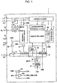
- the count value of the address counter 2 is initialized to a predetermined value based on the inverted signal of a chip-select input signal CS input to the external terminal P1. Further, the address counter 2 creates updated address data based on a signal input from the AND gate G1. The created address data is input to the row decoder 3 and the column decoder 4.
- the latch circuit 7 outputs read data of the memory cell array 5 to an external terminal P6 after keeping it for a predetermined period of time, which is output from the input/output control circuit 8, based on a control signal from the write/read control circuit 6.
- the latch circuit 7 performs either a latch operation or a through operation depending on the output of the AND gate G4.
- the latch circuit 7 performs the latch operation when the output of the AND gate G4 is at the low level, whereas the latch circuit 7 performs the through operation when the output of the AND gate G4 is at the high level.
- the latch operation is an operation for maintaining the output status.
- the through operation is an operation for sending out the input signal as an output signal as it is.
- the AND gate G2 outputs, to the write/read control circuit 6, a signal which is the conjunction of the output signal from the AND gate G1 and a write/read input signal W/R from the external terminal P3.
- the AND gate G3 outputs, to the write/read control circuit 6, a signal which is the conjunction of the output signal from the AND gate G1 and the inverted signal of the write/read input signal W/R from the external terminal P3.
- Each of the stand-by signals STB1 to STB5 is generated by an AND gate G8 and an inverter INV.
- the stand-by signal STB1 is generated by the AND gate G8, which outputs the conjunction of a stand-by signal STB0 and the write/read input signal W/R.
- the stand-by signals STB2, STB3, and STB5 are generated by the inverter INV, which inverts and outputs the write/read input signal W/R.
- the stand-by signal STB0 becomes the stand-by signal STB4 as it is.
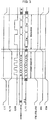
- Fig. 2 is a timing chart for describing a readout operation on the semiconductor integrated circuit.
- Fig.2 shows the chip-select control signal CS, the write/read input signal W/R, the clock CLOCK, the count values of the address counter 2, and the input/output signals I/O at the external terminal P6 in Fig. 1.
- "L" is applied to the external terminal P1, first of all, to initialize the address counter 2.
- "H” is applied to the external terminal P1, and clock pulses for an intended readout start address are input via the external terminal P2.
- "L” for specifying the readout is applied as write/read input signal W/R to the external terminal P3.
- Fig. 3 is a timing chart for describing a write operation on the semiconductor integrated circuit, for example.
- Fig. 3 shows the chip-select control signal CS, the write/read input signal W/R, the clock CLOCK, the count values of the address counter 2, the input/output signals I/O at the external terminal P6 as well as the stand-by signals STB1 to STB5.
- "L" is applied to the external terminal P1 in a condition where the write/read input signal W/R is "L” in order to initialize the address counter 2.
- "H” is applied to the external terminal P1, and clock pulses for an intended write start address are input via the external terminal P2.
- "H" for specifying the write is applied as the write/read input signal W/R to the external terminal P3.
- the buffer B that is another internal circuit is turned to the high-impedance condition by the stand-by signal STB3. Furthermore, the latch circuit 7 is controlled to the latch condition by the stand-by signal STB5. In addition, specification of addresses by the row decoder 3 is suppressed by the stand-by signal STB4.
- a recess 38 is formed at a side of the horizontal wall 35 where an ink supplying outlet is formed such that it is positioned at the center of each cartridge 30 in the width direction, and the circuit substrate 11 is attached here.
- the circuit substrate 11 has a plurality of contacts on a surface facing the contacts of the body and has a memory element on the back surface.
- projections 35a and 35b and overhang portions 35c and 35d are formed on the horizontal wall 35 in order to position the circuit substrate 11.
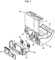
- Fig. 7 is a diagram showing the construction of the carriage shown in Fig. 6.
- levers 51 and 52 are mounted rotatably with respect to axes 49 and 50 as fulcrum at the upper edge of a vertical wall 48 closely facing the ink supply needles 46 and 47 among vertical walls forming the holder 44.
- the remaining amount of ink cartridge can be always monitored.
Landscapes
- Ink Jet (AREA)
- Accessory Devices And Overall Control Thereof (AREA)
Abstract
Description
- Fig. 1
- is a functional block diagram for describing an example of an internal construction of a semiconductor integrated circuit according to the present invention;
- Fig. 2
- is a timing chart for describing a read-out operation on the semiconductor integration circuit;
- Fig. 3
- is a timing chart for describing a write operation and others on the semiconductor integrated circuit;
- Fig. 4
- is a diagram showing a circuit substrate on which one embodiment of the semiconductor integrated circuit is implemented;
- Fig. 5
- is a diagram showing a condition where the circuit substrate shown in Fig. 4 is provided on an ink cartridge;
- Fig. 6
- is a diagram showing an overview of an inkjet printer to which the ink cartridge shown in Fig. 5 is attached;
- Fig. 7
- is a diagram showing a construction of a carriage shown in Fig. 6.
- Fig. 8
- is a diagram showing a condition before an ink cartridge is attached to a holder; and
- Fig. 9
- is a diagram showing a condition where an ink cartridge is attached to a holder.
Claims (11)
- A semiconductor integrated circuit having a low power consumption mode in which the power consumption is lower than in a regular operation mode performing a regular operation and being provided in an ink cartridge, said semiconductor integrated circuit comprising control means for controlling a shift to said low power consumption mode in response to an end of a printing operation using said ink cartridge.
- A semiconductor integrated circuit according to claim 1, further comprising storage means for storing predetermined data at specified addresses, and address creating means for sequentially creating addresses specified for said storage means, wherein said address is initialized when shifting to the low power consumption mode responsive to said control means.
- A semiconductor integrated circuit according to claim 2, wherein the operation of internal circuits is terminated in the low power consumption mode caused by said control means.
- A semiconductor integrated circuit according to claim 3, wherein said internal circuit is a sense amplifier for creating a signal upon reading out data stored in said storage means.
- A semiconductor integrated circuit according to claim 3 wherein said internal circuit is an address decoder for specifying an address in said storage means.
- A semiconductor integrated circuit according to claim 3 wherein said internal circuit is a buffer used for reading out data read out from said storage means.
- A semiconductor integrated circuit according to claim 3 wherein said internal circuit is a latch circuit for latching data read out from said storage means.
- A semiconductor integrated circuit according to claim 1 wherein a shift to the low power consumption mode by said control means and an initialization of address created by said address creating means are performed based on a control signal input to a common external terminal.
- A semiconductor integrated circuit according to claim 8 wherein said common external terminal is a chip-select terminal.
- An ink cartridge having a semiconductor integrated circuit according to any one of claims 1 to 9, for storing at least the remaining amount of ink.
- An inkjet recording device having an ink cartridge according to claim 10 for printing desired image information by using ink supplied from the ink cartridge.
Applications Claiming Priority (3)
| Application Number | Priority Date | Filing Date | Title |
|---|---|---|---|
| JP28324399 | 1999-10-04 | ||
| JP28324399 | 1999-10-04 | ||
| PCT/JP2000/006934 WO2001026114A1 (en) | 1999-10-04 | 2000-10-04 | Integrated circuit, ink cartridge, and ink-jet printer |
Publications (3)
| Publication Number | Publication Date |
|---|---|
| EP1156489A1 true EP1156489A1 (en) | 2001-11-21 |
| EP1156489A4 EP1156489A4 (en) | 2002-10-16 |
| EP1156489B1 EP1156489B1 (en) | 2004-12-29 |
Family
ID=17662953
Family Applications (1)
| Application Number | Title | Priority Date | Filing Date |
|---|---|---|---|
| EP00964673A Expired - Lifetime EP1156489B1 (en) | 1999-10-04 | 2000-10-04 | Integrated circuit, ink cartridge, and ink-jet printer |
Country Status (8)
| Country | Link |
|---|---|
| US (1) | US6655768B1 (en) |
| EP (1) | EP1156489B1 (en) |
| JP (1) | JP3922023B2 (en) |
| KR (1) | KR100429941B1 (en) |
| CN (1) | CN1175426C (en) |
| DE (1) | DE60017096T2 (en) |
| ES (1) | ES2231266T3 (en) |
| WO (1) | WO2001026114A1 (en) |
Cited By (8)
| Publication number | Priority date | Publication date | Assignee | Title |
|---|---|---|---|---|
| CN101060007B (en) * | 2006-04-17 | 2010-10-06 | 科统科技股份有限公司 | composite memory chip |
| WO2013030900A1 (en) * | 2011-08-30 | 2013-03-07 | Brother Kogyo Kabushiki Kaisha | Printing fluid cartridge, printing apparatus, and use of printing fluid cartridge |
| EP2607084A1 (en) * | 2011-12-22 | 2013-06-26 | Brother Kogyo Kabushiki Kaisha | Printing fluid cartridge and printing apparatus |
| EP2607082A1 (en) * | 2011-12-22 | 2013-06-26 | Brother Kogyo Kabushiki Kaisha | Printing fluid cartridge, printing apparatus, and use of printing fluid cartridge |
| US8596772B2 (en) | 2011-08-30 | 2013-12-03 | Brother Kogyo Kabushiki Kaisha | Printing fluid cartridge, printing apparatus, and use of printing fluid cartridge |
| US8678573B2 (en) | 2011-12-22 | 2014-03-25 | Brother Kogyo Kabushiki Kaisha | Printing fluid cartridge |
| EP3038336A4 (en) * | 2013-09-24 | 2016-11-16 | Apex Microelectronics Co Ltd | CHIP, IMAGING BOX, AND COMMUNICATION METHOD FOR CHIP AND IMAGING DEVICE |
| WO2020162931A1 (en) * | 2019-02-06 | 2020-08-13 | Hewlett-Packard Development Company, L.P. | Integrated circuits including customization bits |
Families Citing this family (10)
| Publication number | Priority date | Publication date | Assignee | Title |
|---|---|---|---|---|
| US7181572B2 (en) * | 2002-12-02 | 2007-02-20 | Silverbrook Research Pty Ltd | Cache updating method and apparatus |
| US20090319802A1 (en) * | 2002-12-02 | 2009-12-24 | Silverbrook Research Pty Ltd | Key Genaration In An Integrated Circuit |
| JP4737430B2 (en) * | 2006-06-22 | 2011-08-03 | セイコーエプソン株式会社 | Carriage device, recording device, liquid ejecting device |
| US8023842B2 (en) * | 2010-01-26 | 2011-09-20 | Ricoh Company, Ltd | Methods and apparatus for adjusting printing device power consumption based on usage data |
| CN201645994U (en) * | 2010-02-05 | 2010-11-24 | 珠海纳思达电子科技有限公司 | Ink cartridge for inkjet printer |
| ES2711352T3 (en) | 2010-06-11 | 2019-05-03 | Ricoh Co Ltd | Information storage device, removable device, developer container and image forming device |
| CN104802539B (en) * | 2014-01-29 | 2018-01-09 | 珠海艾派克微电子有限公司 | The feeding assembly and its chip of imaging device, slave addresses update method |
| CN104952485B (en) * | 2014-11-28 | 2019-07-19 | 珠海艾派克微电子有限公司 | A kind of resistance switching circuit, storage circuit and consumable chip |
| JP7151416B2 (en) * | 2018-11-22 | 2022-10-12 | セイコーエプソン株式会社 | DRIVE CIRCUIT, LIQUID EJECTING APPARATUS, AND DRIVING METHOD |
| CN120056605B (en) * | 2024-07-16 | 2026-01-06 | 极海微电子股份有限公司 | Chip components and consumable box components |
Family Cites Families (14)
| Publication number | Priority date | Publication date | Assignee | Title |
|---|---|---|---|---|
| JPH05301349A (en) * | 1992-04-24 | 1993-11-16 | Canon Inc | Printer |
| JP2839995B2 (en) | 1992-10-14 | 1998-12-24 | キヤノン株式会社 | Recording device |
| DE69416229T2 (en) | 1993-10-01 | 1999-07-08 | Canon K.K., Tokio/Tokyo | Image recorder |
| JPH07232438A (en) * | 1994-02-25 | 1995-09-05 | Canon Inc | Inkjet recording apparatus, facsimile apparatus, and copying apparatus |
| WO1996005061A1 (en) * | 1994-08-09 | 1996-02-22 | Encad, Inc. | Printer ink cartridge |
| JPH08101609A (en) * | 1994-09-30 | 1996-04-16 | Ricoh Co Ltd | Image forming device |
| US6065824A (en) * | 1994-12-22 | 2000-05-23 | Hewlett-Packard Company | Method and apparatus for storing information on a replaceable ink container |
| US5670906A (en) | 1995-07-05 | 1997-09-23 | Micron Quantum Devices, Inc. | Integrated circuit operable in a mode having extremely low power consumption |
| JPH09116665A (en) * | 1995-10-18 | 1997-05-02 | Canon Inc | Facsimile machine |
| JPH09213092A (en) * | 1996-02-08 | 1997-08-15 | Hitachi Ltd | Semiconductor integrated circuit device |
| US6073204A (en) * | 1997-04-23 | 2000-06-06 | Micron Technology, Inc. | Memory system having flexible architecture and method |
| JP3406790B2 (en) * | 1996-11-25 | 2003-05-12 | 株式会社東芝 | Data transfer system and data transfer method |
| KR100225954B1 (en) * | 1996-12-31 | 1999-10-15 | 김영환 | Power Saving Semiconductor Memory Devices |
| KR100209509B1 (en) * | 1997-04-28 | 1999-07-15 | 윤종용 | Power saving ink-jet printer |
-
2000
- 2000-10-04 US US09/857,472 patent/US6655768B1/en not_active Expired - Lifetime
- 2000-10-04 WO PCT/JP2000/006934 patent/WO2001026114A1/en not_active Ceased
- 2000-10-04 KR KR10-2001-7006979A patent/KR100429941B1/en not_active Expired - Fee Related
- 2000-10-04 EP EP00964673A patent/EP1156489B1/en not_active Expired - Lifetime
- 2000-10-04 ES ES00964673T patent/ES2231266T3/en not_active Expired - Lifetime
- 2000-10-04 JP JP2001528989A patent/JP3922023B2/en not_active Expired - Fee Related
- 2000-10-04 DE DE60017096T patent/DE60017096T2/en not_active Expired - Lifetime
- 2000-10-04 CN CNB008034656A patent/CN1175426C/en not_active Expired - Fee Related
Cited By (21)
| Publication number | Priority date | Publication date | Assignee | Title |
|---|---|---|---|---|
| CN101060007B (en) * | 2006-04-17 | 2010-10-06 | 科统科技股份有限公司 | composite memory chip |
| US9193167B2 (en) | 2011-08-30 | 2015-11-24 | Brother Kogyo Kabushiki Kaisha | Printing fluid cartridge, printing apparatus, and use of printing fluid cartridge |
| WO2013030900A1 (en) * | 2011-08-30 | 2013-03-07 | Brother Kogyo Kabushiki Kaisha | Printing fluid cartridge, printing apparatus, and use of printing fluid cartridge |
| US10220630B2 (en) | 2011-08-30 | 2019-03-05 | Brother Kogyo Kabushiki Kaisha | Printing fluid cartridge, printing apparatus, and use of printing fluid cartridge |
| US9782974B2 (en) | 2011-08-30 | 2017-10-10 | Brother Kogyo Kabushiki Kaisha | Printing fluid cartridge, printing apparatus, and use of printing fluid cartridge |
| US8596772B2 (en) | 2011-08-30 | 2013-12-03 | Brother Kogyo Kabushiki Kaisha | Printing fluid cartridge, printing apparatus, and use of printing fluid cartridge |
| US8651639B2 (en) | 2011-08-30 | 2014-02-18 | Brother Kogyo Kabushiki Kaisha | Printing fluid cartridge, printing apparatus, and use of printing fluid cartridge |
| EP2910379A3 (en) * | 2011-12-22 | 2016-06-08 | Brother Kogyo Kabushiki Kaisha | Printing fluid cartridge, printing apparatus, and use of printing fluid cartridge |
| EP3597437A1 (en) * | 2011-12-22 | 2020-01-22 | Brother Kogyo Kabushiki Kaisha | Printing fluid cartridge, printing apparatus, and use of printing fluid cartridge |
| EP2803490A3 (en) * | 2011-12-22 | 2016-05-25 | Brother Kogyo Kabushiki Kaisha | Printing fluid cartridge and printing apparatus |
| US8678573B2 (en) | 2011-12-22 | 2014-03-25 | Brother Kogyo Kabushiki Kaisha | Printing fluid cartridge |
| EP2805827A3 (en) * | 2011-12-22 | 2016-05-25 | Brother Kogyo Kabushiki Kaisha | Printing fluid cartridge, printing apparatus, and use of printing fluid cartridge |
| EP2607082A1 (en) * | 2011-12-22 | 2013-06-26 | Brother Kogyo Kabushiki Kaisha | Printing fluid cartridge, printing apparatus, and use of printing fluid cartridge |
| EP3354468A1 (en) * | 2011-12-22 | 2018-08-01 | Brother Kogyo Kabushiki Kaisha | Printing fluid cartridge and printing apparatus |
| EP2607084A1 (en) * | 2011-12-22 | 2013-06-26 | Brother Kogyo Kabushiki Kaisha | Printing fluid cartridge and printing apparatus |
| EP3480022A1 (en) * | 2011-12-22 | 2019-05-08 | Brother Kogyo Kabushiki Kaisha | Printing fluid cartridge and printing apparatus |
| EP3038336A4 (en) * | 2013-09-24 | 2016-11-16 | Apex Microelectronics Co Ltd | CHIP, IMAGING BOX, AND COMMUNICATION METHOD FOR CHIP AND IMAGING DEVICE |
| WO2020162931A1 (en) * | 2019-02-06 | 2020-08-13 | Hewlett-Packard Development Company, L.P. | Integrated circuits including customization bits |
| CN113412201A (en) * | 2019-02-06 | 2021-09-17 | 惠普发展公司,有限责任合伙企业 | Integrated circuit including custom bits |
| AU2019428714B2 (en) * | 2019-02-06 | 2023-03-16 | Hewlett-Packard Development Company, L.P. | Integrated circuits including customization bits |
| US11731419B2 (en) | 2019-02-06 | 2023-08-22 | Hewlett-Packard Development Company, L.P. | Integrated circuits including customization bits |
Also Published As
| Publication number | Publication date |
|---|---|
| KR20010080683A (en) | 2001-08-22 |
| DE60017096D1 (en) | 2005-02-03 |
| EP1156489A4 (en) | 2002-10-16 |
| CN1339161A (en) | 2002-03-06 |
| EP1156489B1 (en) | 2004-12-29 |
| US6655768B1 (en) | 2003-12-02 |
| KR100429941B1 (en) | 2004-05-03 |
| DE60017096T2 (en) | 2005-12-08 |
| ES2231266T3 (en) | 2005-05-16 |
| WO2001026114A1 (en) | 2001-04-12 |
| CN1175426C (en) | 2004-11-10 |
| JP3922023B2 (en) | 2007-05-30 |
Similar Documents
| Publication | Publication Date | Title |
|---|---|---|
| EP1156489B1 (en) | Integrated circuit, ink cartridge, and ink-jet printer | |
| JPWO2001026114A1 (en) | Semiconductor integrated circuit, ink cartridge and inkjet recording device | |
| KR100656111B1 (en) | Ink cartridges, carriage assemblies and ink cartridge systems for ink jet recorders | |
| KR100546949B1 (en) | Recording device, semiconductor device and recording head device | |
| JP4013548B2 (en) | Semiconductor integrated circuit, ink cartridge, and ink jet recording apparatus | |
| US20060077215A1 (en) | Head substrate having data memory, printing head, printing apparatus and producing method therefor | |
| JPWO2001026116A1 (en) | Write-protect circuit, semiconductor integrated circuit using the same, ink cartridge having the semiconductor integrated circuit, and ink-jet recording apparatus | |
| EP1156490A1 (en) | Semiconductor integrated circuit, ink cartridge having this semiconductor integrated circuit, and ink jet recording device mounted with this ink cartridge | |
| JP3582471B2 (en) | Semiconductor integrated circuit, ink cartridge having this semiconductor integrated circuit, and ink jet recording apparatus equipped with this ink cartridge | |
| JP2000198202A5 (en) | Head substrate, print head, printing device | |
| CN216783086U (en) | Consumable chip, consumable box and image forming device | |
| CN114987058B (en) | Consumable chip, data reading and writing method thereof and consumable container | |
| JP4670444B2 (en) | Inkjet recording apparatus, semiconductor device, and recording head apparatus | |
| JP4525842B2 (en) | Recording device, semiconductor device, and recording head device | |
| JP2005177993A (en) | Printing apparatus, printing agent storage container for the apparatus, and printing system | |
| KR19990047942A (en) | Semiconductor memory |
Legal Events
| Date | Code | Title | Description |
|---|---|---|---|
| PUAI | Public reference made under article 153(3) epc to a published international application that has entered the european phase |
Free format text: ORIGINAL CODE: 0009012 |
|
| 17P | Request for examination filed |
Effective date: 20010704 |
|
| AK | Designated contracting states |
Kind code of ref document: A1 Designated state(s): AT BE CH CY DE DK ES FI FR GB GR IE IT LI LU MC NL PT SE |
|
| AX | Request for extension of the european patent |
Free format text: AL;LT;LV;MK;RO;SI |
|
| A4 | Supplementary search report drawn up and despatched |
Effective date: 20020904 |
|
| AK | Designated contracting states |
Kind code of ref document: A4 Designated state(s): AT BE CH CY DE DK ES FI FR GB GR IE IT LI LU MC NL PT SE |
|
| 17Q | First examination report despatched |
Effective date: 20030124 |
|
| RBV | Designated contracting states (corrected) |
Designated state(s): DE ES FR GB IT |
|
| GRAP | Despatch of communication of intention to grant a patent |
Free format text: ORIGINAL CODE: EPIDOSNIGR1 |
|
| GRAS | Grant fee paid |
Free format text: ORIGINAL CODE: EPIDOSNIGR3 |
|
| GRAA | (expected) grant |
Free format text: ORIGINAL CODE: 0009210 |
|
| AK | Designated contracting states |
Kind code of ref document: B1 Designated state(s): DE ES FR GB IT |
|
| REG | Reference to a national code |
Ref country code: GB Ref legal event code: FG4D |
|
| REG | Reference to a national code |
Ref country code: IE Ref legal event code: FG4D |
|
| REF | Corresponds to: |
Ref document number: 60017096 Country of ref document: DE Date of ref document: 20050203 Kind code of ref document: P |
|
| REG | Reference to a national code |
Ref country code: ES Ref legal event code: FG2A Ref document number: 2231266 Country of ref document: ES Kind code of ref document: T3 |
|
| PLBE | No opposition filed within time limit |
Free format text: ORIGINAL CODE: 0009261 |
|
| STAA | Information on the status of an ep patent application or granted ep patent |
Free format text: STATUS: NO OPPOSITION FILED WITHIN TIME LIMIT |
|
| ET | Fr: translation filed | ||
| 26N | No opposition filed |
Effective date: 20050930 |
|
| PGFP | Annual fee paid to national office [announced via postgrant information from national office to epo] |
Ref country code: IT Payment date: 20101018 Year of fee payment: 11 |
|
| PGFP | Annual fee paid to national office [announced via postgrant information from national office to epo] |
Ref country code: ES Payment date: 20101026 Year of fee payment: 11 |
|
| PG25 | Lapsed in a contracting state [announced via postgrant information from national office to epo] |
Ref country code: IT Free format text: LAPSE BECAUSE OF NON-PAYMENT OF DUE FEES Effective date: 20111004 |
|
| PGFP | Annual fee paid to national office [announced via postgrant information from national office to epo] |
Ref country code: FR Payment date: 20121018 Year of fee payment: 13 Ref country code: DE Payment date: 20120927 Year of fee payment: 13 |
|
| PGFP | Annual fee paid to national office [announced via postgrant information from national office to epo] |
Ref country code: GB Payment date: 20121003 Year of fee payment: 13 |
|
| REG | Reference to a national code |
Ref country code: ES Ref legal event code: FD2A Effective date: 20130826 |
|
| PG25 | Lapsed in a contracting state [announced via postgrant information from national office to epo] |
Ref country code: ES Free format text: LAPSE BECAUSE OF NON-PAYMENT OF DUE FEES Effective date: 20111005 |
|
| GBPC | Gb: european patent ceased through non-payment of renewal fee |
Effective date: 20131004 |
|
| PG25 | Lapsed in a contracting state [announced via postgrant information from national office to epo] |
Ref country code: GB Free format text: LAPSE BECAUSE OF NON-PAYMENT OF DUE FEES Effective date: 20131004 |
|
| REG | Reference to a national code |
Ref country code: FR Ref legal event code: ST Effective date: 20140630 |
|
| REG | Reference to a national code |
Ref country code: DE Ref legal event code: R119 Ref document number: 60017096 Country of ref document: DE Effective date: 20140501 |
|
| PG25 | Lapsed in a contracting state [announced via postgrant information from national office to epo] |
Ref country code: DE Free format text: LAPSE BECAUSE OF NON-PAYMENT OF DUE FEES Effective date: 20140501 Ref country code: FR Free format text: LAPSE BECAUSE OF NON-PAYMENT OF DUE FEES Effective date: 20131031 |