EP1155494B1 - Gleichrichteranordnung, vorzugsweise für einen drehstromgenerator für kraftfahrzeuge - Google Patents
Gleichrichteranordnung, vorzugsweise für einen drehstromgenerator für kraftfahrzeuge Download PDFInfo
- Publication number
- EP1155494B1 EP1155494B1 EP00909057A EP00909057A EP1155494B1 EP 1155494 B1 EP1155494 B1 EP 1155494B1 EP 00909057 A EP00909057 A EP 00909057A EP 00909057 A EP00909057 A EP 00909057A EP 1155494 B1 EP1155494 B1 EP 1155494B1
- Authority
- EP
- European Patent Office
- Prior art keywords
- diode
- rectifier
- diodes
- voltage
- semiconductor
- Prior art date
- Legal status (The legal status is an assumption and is not a legal conclusion. Google has not performed a legal analysis and makes no representation as to the accuracy of the status listed.)
- Expired - Lifetime
Links
- 239000004065 semiconductor Substances 0.000 claims description 23
- 230000015556 catabolic process Effects 0.000 description 23
- 238000001816 cooling Methods 0.000 description 8
- 230000000903 blocking effect Effects 0.000 description 6
- 238000010586 diagram Methods 0.000 description 4
- 238000004519 manufacturing process Methods 0.000 description 2
- 229910000679 solder Inorganic materials 0.000 description 2
- 230000006641 stabilisation Effects 0.000 description 2
- 238000011105 stabilization Methods 0.000 description 2
- YZSCPLGKKMSBMV-UHFFFAOYSA-N 5-fluoro-4-(8-fluoro-4-propan-2-yl-2,3-dihydro-1,4-benzoxazin-6-yl)-N-[5-(1-methylpiperidin-4-yl)pyridin-2-yl]pyrimidin-2-amine Chemical compound FC=1C(=NC(=NC=1)NC1=NC=C(C=C1)C1CCN(CC1)C)C1=CC2=C(OCCN2C(C)C)C(=C1)F YZSCPLGKKMSBMV-UHFFFAOYSA-N 0.000 description 1
- XAGFODPZIPBFFR-UHFFFAOYSA-N aluminium Chemical compound [Al] XAGFODPZIPBFFR-UHFFFAOYSA-N 0.000 description 1
- 229910052782 aluminium Inorganic materials 0.000 description 1
- 230000000712 assembly Effects 0.000 description 1
- 238000000429 assembly Methods 0.000 description 1
- 230000001419 dependent effect Effects 0.000 description 1
- 238000010438 heat treatment Methods 0.000 description 1
- 238000002347 injection Methods 0.000 description 1
- 239000007924 injection Substances 0.000 description 1
- 238000009428 plumbing Methods 0.000 description 1
- 230000036544 posture Effects 0.000 description 1
- 238000005476 soldering Methods 0.000 description 1
Images


Classifications
-
- H—ELECTRICITY
- H02—GENERATION; CONVERSION OR DISTRIBUTION OF ELECTRIC POWER
- H02P—CONTROL OR REGULATION OF ELECTRIC MOTORS, ELECTRIC GENERATORS OR DYNAMO-ELECTRIC CONVERTERS; CONTROLLING TRANSFORMERS, REACTORS OR CHOKE COILS
- H02P9/00—Arrangements for controlling electric generators for the purpose of obtaining a desired output
- H02P9/14—Arrangements for controlling electric generators for the purpose of obtaining a desired output by variation of field
- H02P9/26—Arrangements for controlling electric generators for the purpose of obtaining a desired output by variation of field using discharge tubes or semiconductor devices
- H02P9/30—Arrangements for controlling electric generators for the purpose of obtaining a desired output by variation of field using discharge tubes or semiconductor devices using semiconductor devices
-
- H—ELECTRICITY
- H02—GENERATION; CONVERSION OR DISTRIBUTION OF ELECTRIC POWER
- H02M—APPARATUS FOR CONVERSION BETWEEN AC AND AC, BETWEEN AC AND DC, OR BETWEEN DC AND DC, AND FOR USE WITH MAINS OR SIMILAR POWER SUPPLY SYSTEMS; CONVERSION OF DC OR AC INPUT POWER INTO SURGE OUTPUT POWER; CONTROL OR REGULATION THEREOF
- H02M7/00—Conversion of AC power input into DC power output; Conversion of DC power input into AC power output
- H02M7/02—Conversion of AC power input into DC power output without possibility of reversal
- H02M7/04—Conversion of AC power input into DC power output without possibility of reversal by static converters
- H02M7/06—Conversion of AC power input into DC power output without possibility of reversal by static converters using discharge tubes without control electrode or semiconductor devices without control electrode
- H02M7/062—Avoiding or suppressing excessive transient voltages or currents
Definitions
- the invention is based on a three-phase bridge rectifier arrangement according to the genus of Main claim. From DE 42 25 359 C1 are already Three-phase bridge rectifier arrangements with two Semiconductor diodes known per phase, in which the voltage-stabilizing properties of individual Zener diodes are used. With this type of However, voltage stabilization is when the Rectifier arrangement for higher motor vehicle electrical system voltages of 42 volts, for example the manufacturing tolerance of the breakdown voltage the zener diodes too large to be minimal at a given reliable ripple of the voltage Achieve voltage limitation.
- the three-phase bridge rectifier arrangement according to the invention with the distinctive features of the independent has the advantage, even for high Vehicle electrical system voltages provide reliable voltage stabilization to achieve by the bridge rectifier arrangement itself, in particular, for example, at an operating voltage at B + of 42 volts and a maximum ripple at B + of 47 volts reliably achieved a voltage limit as soon as the voltage at B + reaches a value of 55 volts.
- Zener diode pairs it is possible to use high limit voltages with tight Establish tolerance ranges.
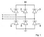
- FIG. 1 shows a known one Rectifier arrangement
- Figure 2 is a first Embodiment
- Figure 3 shows a second Embodiment
- Figure 4 is a current-voltage diagram
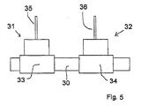
- FIG. 5 shows a further exemplary embodiment.
- Figure 1 shows a known three-phase bridge rectifier arrangement.
- the three connections u, v and w of a three-phase generator are each with a Diode pair (1, 4), (2, 5) or (3, 6) connected, the connections as the center tap of each in series switched diodes are formed.
- the anodes of the diodes 4, 5 and 6 are connected to ground, the cathodes of the diodes 1, 2 and 3 with the positive pole B + of the rectifier arrangement.
- FIG. 1 shows a first invention Embodiment in which the compared to Figure 1 Individual diodes 1 to 6 through pairs 11, 12, 13, 14, 15 and 16 are replaced by series connected diodes, i.e. the Diode pairs put circuit elements in series with two switched p-n junctions.
- the rectifier arrangement allows one (by the coil arrangement of the alternator conditional) ripple of 47 volts at B + and limited at the same time the voltage at B + to a maximum of 55 volts.
- the diodes of the pairs 14, 15 and 16 formed as zener diodes so that between each Combination of two of the three three-phase phases at least one Current path with two anti-serial Zener diode pairs is arranged.
- the Three-phase current ensures that, when appropriate set breakdown voltage of the individual Zener diodes, the operating voltage at B + does not have a value of 55 volts exceeds, if necessary, the relevant Zener diode pair "breaks through", ie the two phases in question shorts.
- the zener diodes instead Zener diode pairs, this is difficult if
- the zener diodes have a maximum ripple Should pass B + of at least 47 volts to B +, but at the same time the specified limit to Voltage limit relatively close to 47 volts (for example the above 55 volts).
- the manufacturing tolerance for breakdown voltages in Zener diodes typically 6 volts, for example covers one Range from 47 to 53 volts.
- the invention Order, on the other hand, avoids these difficulties by the breakdown voltage as the sum of two half as large Breakdown voltages of series connected zener diodes a pair of Zener diodes 14, 15 and 16, respectively is.
- the individual diodes have, for example Breakdown voltage of 24.5 volts on average at one also halved tolerance of +/- 1.5 volts.
- the resulting breakdown voltage of the diode pair is then in a range from 47 volts to 51 volts, so it has one Tolerance range of ⁇ 2 x 3 volts, that's about 4 volts.
- The is a tolerance range reduced by 2 volts a single diode, which in itself is the would provide the required breakdown voltage.
- the diode pairs are 11, 12 and 13 by means of high-blocking single diodes with a Breakdown voltage of, for example, greater than 60 volts replaced.
- the voltage limitation continues to be due to the Zener diode pairs 14, 15 and 16 guaranteed.
- diode pairs 11, 12, and 13 also like the diode pairs 14, 15 and 16 as Zener diode pairs with corresponding breakdown voltage educated.
- Zener diode pairs lie between everyone Combination of two of the three three-phase phases two Current paths, each with two anti-serial connections Zener diode pairs, so that in the event of an overvoltage between two phases of three-phase current opened two breakthrough paths can be, whereby the current per diode is reduced and thus the temperature influence on the breakdown voltage is reduced again.
- FIG 3 shows another invention Embodiment in which the compared to Figure 1 Individual diodes 1 to 3 through high blocking diodes 17, 18 and 19 formed with a breakdown voltage greater than 55 volts and the individual diodes 4 to 6 by semiconductor rectifier elements 20, 21 and 22 are replaced.
- the Rectifier elements 20, 21 and 22 are each through a four-layer diode with cathode short circuit is formed, wherein the anode of each four-layer diode with the ground connection connected is.
- a four-layer diode is known to be by using a pnpn semiconductor layer sequence Cathode short-circuit formed and connected in series of three p-n junctions.
- Each four-layer diode connected in antiparallel between the ground connection and the respective phase connection u, v or w is one high-blocking diode of the type of diodes on the positive pole side B + the rectifier arrangement.
- FIG. 4 a current-voltage diagram (I-U diagram) a a four-layer diode and a current-voltage diagram b a rectifier element 20, 21 or 22.
- I-U diagram current-voltage diagram
- U1 for example 50 volts
- U2 reverse polarity
- the value of the current with this voltage flip is the so-called tipping current.
- the value of the breakover voltage U3 and the Breakdown current can be dimensioned accordingly Four-layer diode can be selected.
- the requirement of a Voltage limitation to 55 volts can with the invention rectifier elements used in the rectifier be easily met.
- the power loss in the direction of flow of the diodes compared to the known structure of Figure 1 by the double the number of diodes, the Power loss due to a smaller number of Diode chips lower.
- the Rectifier function is advantageous that when the Rectifier elements, the voltage drops sharply, thus there is also less power dissipation and thus the Breakdown voltage can be specified more precisely.
- the Rectifier elements 20, 21 and 22 with the high blocking Diodes 17, 18 and 19 can be interchanged. This one too modified arrangement is for any combination of two of the three three-phase phases at least one by two given anti-serial switched rectifier elements Breakdown current path guaranteed.
- the Rectifier elements 20, 21 and 22 instead of through Parallel connection of four-layer diodes ("Thyristor diodes") with high blocking diodes Three-layer diodes (“transistor diodes”) are formed.
- each Rectifier element is therefore a three-layer diode educated.
- a three-layer diode is made by a pnp semiconductor layer sequence with cathode short circuit formed and represents a series connection of two p-n junctions
- a three-layer diode already have an I-U characteristic of form b in FIG additional wiring with a parallel high blocking diode is therefore unnecessary.
- U4 is typically - 15 V.
- for High-voltage on-board electrical system now only six Semiconductor chips needed.
- FIG. 5 shows a side view of the mechanical structure a pair of diodes 11, 12, 13, 14, 15 or 16.
- Each Single diode of a pair of diodes is a press-in diode 31 or 32 with a press-in base 33 or 34 educated.
- the semiconductor chip is inside the Diode housing shown arranged (not shown) and from the outside via the head wire 35 or 36 and the Press-in socket 33 or 34 can be contacted.
- the two Press-in bases are electrically conductive over the Aluminum heat sink 30 connected into which the press-in base two openings adapted to the shape of the press-in base are pressed in.
- the Head wires are electrical according to Figure 2 with the Three-phase connections or the poles (ground connection or B +) connected to the electrical system (not shown in Figure 5).
- the Complete rectifier according to Figure 2 then exposes itself six identical cooling plate arrangements according to FIG. 5 together, the six cooling plates, for example, on one Plastic connection plate fixed and the Connections between the cooling plate arrangements in the plastic be injected.
- the cooling plate arrangement according to FIG. 5 is also for the Realization of a rectifier element 20, 21 or 22 usable according to FIG. 3 by inserting in the press-in diode 31
- Semiconductor chip with a four-layer diode and in the Einpreßdiode 32 is a semiconductor chip with a high blocking Diode is arranged.
- the anode of the diode is for example via the cooling plate with the cathode Four-layer diode electrically connected, the opposite Electrodes must then be connected to each other via the head wires contacted and with the relevant three-phase phase are connected (not shown in Figure 5).
- the mechanical structure of a Diode pair 11 to 16 also without a cooling plate 30 are carried out by a series connection of two Semiconductor diode chips within a single one Diode housing of a press-in diode is arranged.
- Einpreßdiode realized diode pairs in already known To use rectifier cooling plate assemblies by simply the press-in diodes with a single semiconductor chip inside be replaced by the new press-in diodes.
- the Current path through the new injection diodes runs from Press-in base over a solder area to the first diode chip, thence via a further plumbing area which joins the first connects the second diode chip arranged above, to second diode chip and from there via another Solder area to the head wire.
- This structure can be like the known arrangement with only one diode chip in one usual soldering furnace can be soldered.
Landscapes
- Engineering & Computer Science (AREA)
- Power Engineering (AREA)
- Rectifiers (AREA)
Description
Claims (4)
- Dreiphasen-Brückengleichrichteranordnung mit drei Gleichrichterpfaden, in denen jeweils zwei Gleichrichterelemente in Reihe liegen, wobei jeder Gleichrichterpfad zwischen den Gleichrichterelementen mit einer von drei Leitungen eines Drehstromanschlusses (u,v,w) verbindbar ist, wobei die drei dem Drehstromanschluß gegenüberliegenden Kathoden-Anschlüsse der Gleichrichterelemente zu einem Pluspol (B+) und die drei dem Drehstromanschluß gegenüberliegenden Anoden-Anschlüsse der Gleichrichterelemente zu einem Minuspol zusammengeschaltet sind, dadurch gekennzeichnet, daß mindestens drei der Gleichrichterelemente durch zweipolige Halbleitergleichrichter (11, 12, 13, 14, 15, 16; 11, 12, 13, 20, 21, 22) mit mindestens zwei in Reihe geschalteten p-n-Übergangen gebildet werden, wobei die mit dem Pluspol oder die mit dem Minuspol verbundenen Halbleitergleichrichter durch zwei in Reihe geschaltete und als Zenerdioden ausgebildete Halbleiterdioden (11, 12, 13, 14, 15, 16) gebildet werden.
- Gleichrichteranordnung nach Anspruch 1, dadurch gekennzeichnet, daß die mit dem Minuspol verbundenen Halbleitergleichrichter durch jeweils eine Antiparallelschaltung einer Vierschichtdiode mit einer hochsperrenden Diode gebildet werden.
- Gleichrichteranordnung nach einem der Ansprüche 1 oder 2, dadurch gekennzeichnet, daß die mit dem Minuspol verbundenen Halbleitergleichrichter durch jeweils eine Dreischichtdiode gebildet werden.
- Gleichrichteranordnung nach Anspruch 1, dadurch gekennzeichnet, daß die in Reihe geschalteten Halbleiterdioden (11, 12, 13, 14, 15, 16) aus jeweils zwei Halbleiterchips bestehen, wobei die Halbleiterchips aufeinander gelötet und in einem gemeinsamen Diodengehäuse untergebracht sind.
Applications Claiming Priority (3)
| Application Number | Priority Date | Filing Date | Title |
|---|---|---|---|
| DE19908697 | 1999-02-26 | ||
| DE19908697A DE19908697A1 (de) | 1999-02-26 | 1999-02-26 | Gleichrichteranordnung, vorzugsweise für einen Drehstromgenerator für Kraftfahrzeuge |
| PCT/DE2000/000499 WO2000052814A1 (de) | 1999-02-26 | 2000-02-23 | Gleichrichteranordnung, vorzugsweise für einen drehstromgenerator für kraftfahrzeuge |
Publications (2)
| Publication Number | Publication Date |
|---|---|
| EP1155494A1 EP1155494A1 (de) | 2001-11-21 |
| EP1155494B1 true EP1155494B1 (de) | 2002-10-30 |
Family
ID=7899189
Family Applications (1)
| Application Number | Title | Priority Date | Filing Date |
|---|---|---|---|
| EP00909057A Expired - Lifetime EP1155494B1 (de) | 1999-02-26 | 2000-02-23 | Gleichrichteranordnung, vorzugsweise für einen drehstromgenerator für kraftfahrzeuge |
Country Status (8)
| Country | Link |
|---|---|
| US (1) | US6538910B1 (de) |
| EP (1) | EP1155494B1 (de) |
| JP (1) | JP4510298B2 (de) |
| KR (1) | KR100758834B1 (de) |
| BR (1) | BR0008486A (de) |
| DE (2) | DE19908697A1 (de) |
| ES (1) | ES2185571T3 (de) |
| WO (1) | WO2000052814A1 (de) |
Families Citing this family (17)
| Publication number | Priority date | Publication date | Assignee | Title |
|---|---|---|---|---|
| DE10005183A1 (de) | 2000-02-05 | 2001-08-09 | Bosch Gmbh Robert | Gleichrichteranordnung |
| US20040151765A1 (en) * | 2001-09-18 | 2004-08-05 | Ritchie Branson W. | Methods and compositions for wound management |
| US20040208842A1 (en) * | 2001-09-18 | 2004-10-21 | Ritchie Branson W. | Antimicrobial cleansing compositions and methods of use |
| DE10102408A1 (de) * | 2001-01-15 | 2002-07-18 | Dietrich Eckert | Verfahren für Drehstromanschluß für EVG |
| RU2206172C2 (ru) * | 2001-04-09 | 2003-06-10 | Мордовский государственный университет им. Н.П.Огарева | Преобразователь трехфазного переменного напряжения в постоянное |
| DE10330258A1 (de) * | 2003-07-04 | 2005-01-20 | Robert Bosch Gmbh | Gleichrichteranordnung mit unterschiedlichen Gleichrichterelementen |
| US20070185202A1 (en) * | 2004-03-03 | 2007-08-09 | University Of Georgia Research Foundation, Inc. | Methods and compositions for ophthalmic treatment of fungal and bacterial infections |
| US7732974B1 (en) | 2006-11-15 | 2010-06-08 | Justin Boland | Electrostatic power generator cell and method of manufacture |
| EP2026454A1 (de) * | 2007-08-17 | 2009-02-18 | Siemens Aktiengesellschaft | Ein-Fehler-sichere Brückengleichrichtung |
| US20090052134A1 (en) * | 2007-08-22 | 2009-02-26 | Casteel Jordan B | Liquid-cooled grounded heatsink for diode rectifier system |
| JP5649473B2 (ja) * | 2011-01-26 | 2015-01-07 | 東芝三菱電機産業システム株式会社 | 電力変換装置の保護装置 |
| CN103236685A (zh) * | 2013-05-17 | 2013-08-07 | 安徽一天电气技术有限公司 | 整流型阻容吸收装置 |
| RU2534041C1 (ru) * | 2013-05-27 | 2014-11-27 | Негосударственное образовательное учреждение "Саранский Дом науки и техники Российского Союза научных и инженерных общественных организаций" (НОУ "СДНиТ") | Преобразователь трехфазного переменного напряжения в постоянное |
| WO2018141342A1 (en) * | 2017-01-31 | 2018-08-09 | Vestas Wind Systems A/S | Dc-dc converter and dc-dc conversion method |
| US20190326828A1 (en) * | 2018-04-19 | 2019-10-24 | Hamilton Sundstrand Corporation | Fault tolerant ac rectification |
| US11990181B2 (en) * | 2021-06-22 | 2024-05-21 | Untether Ai Corporation | Low-power static random access memory |
| EP4212891A1 (de) | 2022-01-08 | 2023-07-19 | Goodrich Aerospace Services Private Limited | Fehlererkennungsverfahren und systeme dafür |
Family Cites Families (9)
| Publication number | Priority date | Publication date | Assignee | Title |
|---|---|---|---|---|
| US3087106A (en) * | 1960-07-18 | 1963-04-23 | Allis Chalmers Mfg Co | Surge controller for protecting a source of electrical energy |
| US3739209A (en) | 1972-08-31 | 1973-06-12 | Gen Motors Corp | Rectifier assembly |
| GB8518409D0 (en) | 1985-07-22 | 1985-08-29 | Lee G T | Automobile electric power generation |
| US4866344A (en) * | 1986-09-19 | 1989-09-12 | Varian Associates, Inc. | High voltage power supply for a microwave electron tube |
| JPH02185069A (ja) * | 1988-12-02 | 1990-07-19 | Motorola Inc | 高エネルギー阻止能力及び温度補償された阻止電圧を具備する半導体デバイス |
| JPH04308430A (ja) * | 1991-04-03 | 1992-10-30 | Nippondenso Co Ltd | 二出力型電源装置 |
| CA2054319C (en) | 1991-06-28 | 1995-01-17 | Hirokazu Ioroi | Power supply unit for arc processing |
| DE4225359C1 (de) | 1992-07-31 | 1994-03-31 | Audi Ag | Drehstromgenerator mit Gleichrichter, insbesondere für ein Kraftfahrzeug |
| JP3429434B2 (ja) * | 1997-06-13 | 2003-07-22 | 新電元工業株式会社 | バッテリ電圧調整装置 |
-
1999
- 1999-02-26 DE DE19908697A patent/DE19908697A1/de not_active Ceased
-
2000
- 2000-02-23 KR KR1020017010841A patent/KR100758834B1/ko not_active Expired - Fee Related
- 2000-02-23 US US09/914,406 patent/US6538910B1/en not_active Expired - Fee Related
- 2000-02-23 DE DE50000701T patent/DE50000701D1/de not_active Expired - Lifetime
- 2000-02-23 WO PCT/DE2000/000499 patent/WO2000052814A1/de not_active Ceased
- 2000-02-23 ES ES00909057T patent/ES2185571T3/es not_active Expired - Lifetime
- 2000-02-23 JP JP2000603141A patent/JP4510298B2/ja not_active Expired - Fee Related
- 2000-02-23 EP EP00909057A patent/EP1155494B1/de not_active Expired - Lifetime
- 2000-02-23 BR BR0008486-7A patent/BR0008486A/pt not_active IP Right Cessation
Also Published As
| Publication number | Publication date |
|---|---|
| KR100758834B1 (ko) | 2007-09-19 |
| JP2002538756A (ja) | 2002-11-12 |
| JP4510298B2 (ja) | 2010-07-21 |
| ES2185571T3 (es) | 2003-05-01 |
| WO2000052814A1 (de) | 2000-09-08 |
| EP1155494A1 (de) | 2001-11-21 |
| US6538910B1 (en) | 2003-03-25 |
| BR0008486A (pt) | 2002-02-05 |
| KR20010102391A (ko) | 2001-11-15 |
| DE50000701D1 (de) | 2002-12-05 |
| DE19908697A1 (de) | 2000-09-07 |
Similar Documents
| Publication | Publication Date | Title |
|---|---|---|
| DE69607965T2 (de) | Wandlerschaltung, schaltung mit wenigstens einem schalter und schaltungsmodul | |
| DE3615052C2 (de) | ||
| DE19908697A1 (de) | Gleichrichteranordnung, vorzugsweise für einen Drehstromgenerator für Kraftfahrzeuge | |
| EP1815586B1 (de) | Umrichterschaltung zur schaltung einer vielzahl von schaltspannungsniveaus | |
| DE10308313B4 (de) | Halbleiterdiode, elektronisches Bauteil, Spannungszwischenkreisumrichter und Steuerverfahren | |
| DE3521079A1 (de) | Rueckwaerts leitende vollsteuergate-thyristoranordnung | |
| DE102021202174A1 (de) | Leistungsmodul, insbesondere für einen Wechselrichter für Elektromaschinen | |
| DE1464983B1 (de) | In zwei Richtungen schaltbares und steuerbares Halbleiterbauelement | |
| DE3741394A1 (de) | Schaltungsanordnung zum schutz vor verpolungsschaeden fuer lastkreise mit einem mos-fet als schalttransistor | |
| DE3518478A1 (de) | Inverter | |
| DE19523095A1 (de) | Stromrichterschaltungsanordnung | |
| DE3131894A1 (de) | Zuendschaltung fuer einen leistungsthyristor | |
| EP0500032B1 (de) | Stromrichterschaltungsanordnung und ihre Verwendung | |
| EP0008008B1 (de) | Thyristor | |
| DE102005047101B3 (de) | Halbleiterschalteranordnung und Ansteuerverfahren | |
| DE2149038C2 (de) | Halbleiterbauelement und Verfahren zum Betrieb des Halbleiterbauelements | |
| DE3234602C2 (de) | ||
| DE10256121A1 (de) | Umschaltbarer Gleichstromwandler für ein Netz mit zwei Spannungen und ein Netz mit zwei Spannungen, das mit einem derartigen Wandler ausgestattet ist | |
| DE102012216185A1 (de) | Begrenzerschaltung für einen Halbleitertransistor und Verfahren zum Begrenzen der Spannung über einen Halbleitertransistor | |
| DE4042378C2 (de) | ||
| DE19648948C1 (de) | Wechselrichter mit Bremssteller | |
| DE3542570A1 (de) | Gate-turnoff-thyristor mit integrierter antiparalleler diode | |
| DE2707988C2 (de) | ||
| DE3615049C2 (de) | Integrierte Widerstandsanordnung mit Schutzelement gegen Verpolung und Über- bzw. Unterspannung | |
| DE3430308A1 (de) | Stromrichter |
Legal Events
| Date | Code | Title | Description |
|---|---|---|---|
| PUAI | Public reference made under article 153(3) epc to a published international application that has entered the european phase |
Free format text: ORIGINAL CODE: 0009012 |
|
| 17P | Request for examination filed |
Effective date: 20010926 |
|
| AK | Designated contracting states |
Kind code of ref document: A1 Designated state(s): AT BE CH CY DE DK ES FI FR GB GR IE IT LI LU MC NL PT SE |
|
| GRAG | Despatch of communication of intention to grant |
Free format text: ORIGINAL CODE: EPIDOS AGRA |
|
| 17Q | First examination report despatched |
Effective date: 20020114 |
|
| GRAG | Despatch of communication of intention to grant |
Free format text: ORIGINAL CODE: EPIDOS AGRA |
|
| GRAH | Despatch of communication of intention to grant a patent |
Free format text: ORIGINAL CODE: EPIDOS IGRA |
|
| GRAH | Despatch of communication of intention to grant a patent |
Free format text: ORIGINAL CODE: EPIDOS IGRA |
|
| GRAA | (expected) grant |
Free format text: ORIGINAL CODE: 0009210 |
|
| AK | Designated contracting states |
Kind code of ref document: B1 Designated state(s): DE ES FR GB IT |
|
| REG | Reference to a national code |
Ref country code: GB Ref legal event code: FG4D Free format text: NOT ENGLISH |
|
| REF | Corresponds to: |
Ref document number: 50000701 Country of ref document: DE Date of ref document: 20021205 |
|
| GBT | Gb: translation of ep patent filed (gb section 77(6)(a)/1977) |
Effective date: 20030218 |
|
| REG | Reference to a national code |
Ref country code: ES Ref legal event code: FG2A Ref document number: 2185571 Country of ref document: ES Kind code of ref document: T3 |
|
| ET | Fr: translation filed | ||
| PLBE | No opposition filed within time limit |
Free format text: ORIGINAL CODE: 0009261 |
|
| STAA | Information on the status of an ep patent application or granted ep patent |
Free format text: STATUS: NO OPPOSITION FILED WITHIN TIME LIMIT |
|
| 26N | No opposition filed |
Effective date: 20030731 |
|
| PGFP | Annual fee paid to national office [announced via postgrant information from national office to epo] |
Ref country code: GB Payment date: 20050211 Year of fee payment: 6 |
|
| PGFP | Annual fee paid to national office [announced via postgrant information from national office to epo] |
Ref country code: ES Payment date: 20050224 Year of fee payment: 6 |
|
| PG25 | Lapsed in a contracting state [announced via postgrant information from national office to epo] |
Ref country code: GB Free format text: LAPSE BECAUSE OF NON-PAYMENT OF DUE FEES Effective date: 20060223 |
|
| PG25 | Lapsed in a contracting state [announced via postgrant information from national office to epo] |
Ref country code: ES Free format text: LAPSE BECAUSE OF NON-PAYMENT OF DUE FEES Effective date: 20060224 |
|
| GBPC | Gb: european patent ceased through non-payment of renewal fee |
Effective date: 20060223 |
|
| REG | Reference to a national code |
Ref country code: ES Ref legal event code: FD2A Effective date: 20060224 |
|
| PGFP | Annual fee paid to national office [announced via postgrant information from national office to epo] |
Ref country code: IT Payment date: 20110226 Year of fee payment: 12 |
|
| PG25 | Lapsed in a contracting state [announced via postgrant information from national office to epo] |
Ref country code: IT Free format text: LAPSE BECAUSE OF NON-PAYMENT OF DUE FEES Effective date: 20120223 |
|
| REG | Reference to a national code |
Ref country code: DE Ref legal event code: R084 Ref document number: 50000701 Country of ref document: DE Effective date: 20140508 |
|
| REG | Reference to a national code |
Ref country code: FR Ref legal event code: PLFP Year of fee payment: 17 |
|
| REG | Reference to a national code |
Ref country code: FR Ref legal event code: PLFP Year of fee payment: 18 |
|
| REG | Reference to a national code |
Ref country code: FR Ref legal event code: PLFP Year of fee payment: 19 |
|
| PGFP | Annual fee paid to national office [announced via postgrant information from national office to epo] |
Ref country code: FR Payment date: 20190221 Year of fee payment: 20 |
|
| PGFP | Annual fee paid to national office [announced via postgrant information from national office to epo] |
Ref country code: DE Payment date: 20190423 Year of fee payment: 20 |
|
| REG | Reference to a national code |
Ref country code: DE Ref legal event code: R071 Ref document number: 50000701 Country of ref document: DE |