EP1154561A2 - Microwave oscillator and low-noise converter using the same - Google Patents
Microwave oscillator and low-noise converter using the same Download PDFInfo
- Publication number
- EP1154561A2 EP1154561A2 EP01108601A EP01108601A EP1154561A2 EP 1154561 A2 EP1154561 A2 EP 1154561A2 EP 01108601 A EP01108601 A EP 01108601A EP 01108601 A EP01108601 A EP 01108601A EP 1154561 A2 EP1154561 A2 EP 1154561A2
- Authority
- EP
- European Patent Office
- Prior art keywords
- microstrip line
- coupled
- msl
- low
- released end
- Prior art date
- Legal status (The legal status is an assumption and is not a legal conclusion. Google has not performed a legal analysis and makes no representation as to the accuracy of the status listed.)
- Granted
Links
Images




Classifications
-
- H—ELECTRICITY
- H03—ELECTRONIC CIRCUITRY
- H03B—GENERATION OF OSCILLATIONS, DIRECTLY OR BY FREQUENCY-CHANGING, BY CIRCUITS EMPLOYING ACTIVE ELEMENTS WHICH OPERATE IN A NON-SWITCHING MANNER; GENERATION OF NOISE BY SUCH CIRCUITS
- H03B5/00—Generation of oscillations using amplifier with regenerative feedback from output to input
- H03B5/18—Generation of oscillations using amplifier with regenerative feedback from output to input with frequency-determining element comprising distributed inductance and capacitance
- H03B5/1864—Generation of oscillations using amplifier with regenerative feedback from output to input with frequency-determining element comprising distributed inductance and capacitance the frequency-determining element being a dielectric resonator
- H03B5/187—Generation of oscillations using amplifier with regenerative feedback from output to input with frequency-determining element comprising distributed inductance and capacitance the frequency-determining element being a dielectric resonator the active element in the amplifier being a semiconductor device
-
- H—ELECTRICITY
- H03—ELECTRONIC CIRCUITRY
- H03B—GENERATION OF OSCILLATIONS, DIRECTLY OR BY FREQUENCY-CHANGING, BY CIRCUITS EMPLOYING ACTIVE ELEMENTS WHICH OPERATE IN A NON-SWITCHING MANNER; GENERATION OF NOISE BY SUCH CIRCUITS
- H03B5/00—Generation of oscillations using amplifier with regenerative feedback from output to input
- H03B5/18—Generation of oscillations using amplifier with regenerative feedback from output to input with frequency-determining element comprising distributed inductance and capacitance
- H03B5/1864—Generation of oscillations using amplifier with regenerative feedback from output to input with frequency-determining element comprising distributed inductance and capacitance the frequency-determining element being a dielectric resonator
Definitions
- the present invention relates to a microwave oscillator stabilized in frequency by using a dielectric resonator, and a low-noise converter (International Patent Classification H01P1/17) incorporated in a radio wave receiving antenna of broadcast or communication satellite.
- a dielectric resonator and a low-noise converter (International Patent Classification H01P1/17) incorporated in a radio wave receiving antenna of broadcast or communication satellite.
- Fig. 6 is a circuit diagram of a microwave oscillator hitherto used as the local oscillator of a low-noise converter.
- a bipolar transistor 1 for microwave oscillation hereinafter the bipolar transistor is called merely as a transistor be distinguished from the field effect transistor or FET
- MSL microstrip line
- a choke circuit composed of high impedance line (HIL) 6a and MSL 4d, and a dc voltage divider composed of dc resistances 3c and 3d are connected serially as shown in the diagram, and one end of the resistance 3c is connected to a bias supply terminal 2b of the transistor, and a bias voltage is applied to the base terminal therefrom.
- HIL high impedance line
- MSL 4d dc voltage divider
- a capacitor 7c for grounding the microwave component leaking out from the HIL 6a is connected parallel to the resistance 3d, and one end is grounded.
- a series circuit of a high frequency resistance 3b and MSL 4c of which one end is released, having a length of ⁇ g/4 is connected as shown in the diagram, and a resistive terminal end is formed in the MSL 4a.
- ⁇ g is the guide wavelength of the MSL 4c corresponding to the oscillation frequency. (Hereinafter, ⁇ g is meant as the guide wavelength determined by the corresponding MSL. The value of ⁇ g varies with the line width of MSL, thickness of circuit board, and dielectric constant.)
- the MSL 4b is connected to the collector of transistor 1, and in this line 4b, a choke circuit of HIL 6b and MSL 4f and a dc resistance 3a are connected as shown in the diagram, and one end of the resistance 3a is connected to a bias supply terminal 2a of the transistor, and a bias voltage is applied to the collector terminal therefrom.
- a capacitor 7b for grounding the microwave component leaking out from the HIL 6b is connected serially to the resistance 3a, and one end is grounded.
- a hollow circular dielectric resonator (DR) 5 couples the MSL 4a and 4b electromagnetically, and is arranged so that the distance from its release end to the closest position to the center of the DR 5 may be ⁇ g/4 on the MSL 4b.
- the oscillation frequency and oscillation power are stabilized at the frequency determined by the resonance frequency of the DR 5, and the oscillation power is delivered from an output terminal 8 through an impedance matching circuit 9 and a dc blocking capacitor 7a connected to the emitter of the transistor 1.
- the HIL 6c and MSL 4e connected to the matching circuit 9 form a choke circuit, and are used for preventing leak of microwave oscillation power and grounding the emitter of the transistor 1 in direct current.
- This conventional configuration requires choke circuits composed of HIL 6a, 6b, 6c and MSL 4d, 4f, 4e which are connected for applying a dc bias to the MSL 4a, 4b connected to the corresponding terminals of the transistor 1 and connected to the impedance matching circuit 9, and these choke circuits make it difficult to reduce the size of the microwave oscillator or induce deterioration of phase noise characteristics, generation of spurious oscillation, or other unstable oscillation.
- the microwave oscillator of the invention is characterized by the configuration in which MSL A released at one end is connected to the base terminal of a transistor, MSL B is connected to the collector terminal, a DR is disposed closely to the MSL A and MSL B to couple them electromagnetically, and a stabilized oscillation output is obtained by inducing parallel feedback from the collector to the base, and further the center of the DR is set closest to the position at which the distance from the released end on the MSL A is ⁇ g1/4, and HIL is merely connected to this position as a bias supply line to the base terminal, and therefore without using choke circuits which occupied a relatively wide area on the conventional circuit board, a small and stable microwave oscillator having excellent phase noise characteristics may be realized.
- ⁇ g1 is the guide wavelength in the MSL A.
- the MSL B connected to the collector terminal of the transistor is also released at one end, and the center of the DR is set closest to the position at which the distance from the released end on the MSL B is ⁇ g2/4, and merely the HIL is connected as a bias supply line to the collector terminal, and therefore without using choke circuits conventionally added to the bias supply lines to both base and collector terminals, the size may be further reduced.
- ⁇ g2 is the guide wavelength in the MSL B.
- MSL A with a released end is connected to its gate terminal
- MSL B is connected to the drain terminal
- a DR is disposed closely to the MSL A and B to couple them electromagnetically, and a stabilized oscillation output is obtained by inducing a parallel feedback from the drain to the gate, and the center of the DR is set closest to the position at which the distance from the released end on the MSL A is ⁇ g1/4, and HIL is merely connected as a bias supply line to the gate terminal, and therefore without using choke circuits which occupied a relatively wide area on the conventional circuit board, a small and stable microwave oscillator having excellent phase noise characteristics may be realized.
- the MSL B connected to the drain terminal of the FET is also released at one end, and the center of the DR is set closest to the position at which the distance from the released end on the MSL B is ⁇ g2/4, and merely the HIL is connected as a bias supply line to the drain terminal, and therefore without using choke circuits conventionally added to the bias supply lines to both gate and drain terminals, the size may be further reduced.
- any one of such microwave oscillators in the local oscillator for the low-noise converter for receiving satellite signal composed of a probe for converting the satellite signal in the circular waveguide obtained from a satellite signal receiving antenna into MSL mode, a low-noise amplifier, a mixer, a local oscillator, and an IF amplifier By using any one of such microwave oscillators in the local oscillator for the low-noise converter for receiving satellite signal composed of a probe for converting the satellite signal in the circular waveguide obtained from a satellite signal receiving antenna into MSL mode, a low-noise amplifier, a mixer, a local oscillator, and an IF amplifier, a small and stable low-noise converter for receiving satellite signal having excellent phase noise characteristics may be realized.
- FIG. 1 A circuit diagram of a microwave oscillator in embodiment 1 of the invention is shown in Fig. 1.
- MSL 4a with a released end is connected, and HIL 6a and dc resistance 3b are connected serially to the side of line 4a as shown in Fig. 1, one end of the resistance 3b is connected to a bias voltage supply terminal 2 through dc resistance 3a, and a bias voltage is applied to the base terminal therefrom.
- MSL 4b with a released end is connected, and HIL 6b and dc resistance 3a are connected serially to the side of line 4b as shown in Fig. 1, and led to the bias voltage supply terminal 2, and a bias voltage is applied to the collector terminal therefrom.
- the emitter terminal is directly grounded.
- a DR 5 is disposed so that the position at which the distance from the released end on the MSL 4a and MSL 4b lines is L1 and L2 may be closest to the center of the DR 5.
- L1 and L2 respectively at ⁇ g1/4 and ⁇ g2/4 ( ⁇ g1 and ⁇ g2 are guide wavelengths of MSL 4a and MSL 4b respectively at the resonance frequency of DR 5)
- the MSL 4b connected to the collector and the MSL 4a connected to the base terminal are electromagnetically coupled through the DR 5, and a parallel feedback is induced between the collector and base of the transistor, and hence a microwave oscillation is stabilized at a desired frequency by the DR 5.
- This oscillation power is obtained from an output terminal 8 through a dc blocking capacitor 7a.
- the impedance of seeing the HIL 6a from the position of Pa is a sufficiently large value as compared with Z(Pa) without using choke circuit with a stab 4d in the prior art shown in Fig. 6, and it is possible to suppress sufficiently leak of the microwave electromagnetic field of the MSL 4a to the HIL 6a. Therefore, a small and stable microwave oscillator having excellent phase noise characteristics may be realized.
- a voltage feedback system is used in the bias method of the transistor 1, but similar effects are obtained by other bias method such as current feedback system.
- same effects are obtained by using interdigital filter by MSL or the like in the dc blocking capacitor 7a.
- a circuit diagram of a microwave oscillator of this embodiment is same as that of embodiment 1 shown in Fig. 1.
- the impedance of seeing the HIL 6b from the position of Pb is, same as in embodiment 1, a sufficiently large value as compared with Z(Pb) without using choke circuit with a stab 4f in the prior art shown in Fig. 5, and it is possible to suppress sufficiently leak of the microwave electromagnetic field of the MSL 4b to the HIL 6b. Therefore, a small and stable microwave oscillator having excellent phase noise characteristics may be realized.
- the bias method of the transistor 1 and dc blocking capacitor 7a may be varied same as in embodiment 1.
- FIG. 2 A circuit diagram of a microwave oscillator in embodiment 3 of the invention is shown in Fig. 2.
- MSL 4a with a released end is connected, and HIL 6a and dc resistance 3e are connected serially to the side of line 4a as shown in Fig. 2, and one end of the resistance 3e is grounded.
- MSL 4b with a released end is connected.
- HIL 6b At a side of the line 4b, as shown in Fig. 2, one end of HIL 6b is connected, and a dc resistance 3c and capacitor 7b are connected to other end, and the resistance 3c is led into a bias voltage supply terminal 2, from which a bias voltage is applied to the FET 9.
- the capacitor 7b is provided for grounding the microwave component leaking out from the HIL 6b.
- a impedance matching circuit 10 is connected, and other end is connected to an output terminal 8 through a dc blocking capacitor 7a.
- a choke circuit composed of HIL 6c and stab 4c and a dc resistance 3d are connected serially, and one end of the resistance 3d is grounded.
- a DR 5 is disposed so that the position at which the distance from the released end on the MSL 4a and MSL 4b lines is L1 and L2 may be closest to the center of the DR 5.
- the impedance of seeing the HIL 6a from the position of Pa is a sufficiently large value as compared with Z(Pa) without using choke circuit with a stab 4d in the prior art shown in Fig. 5, and it is possible to suppress sufficiently leak of the microwave electromagnetic field of the MSL 4a to the HIL 6a. Therefore, a small and stable microwave oscillator having excellent phase noise characteristics may be realized.
- a circuit diagram of a microwave oscillator of this embodiment is same as that of embodiment 3 shown in Fig. 2.
- the impedance of seeing the HIL 6b from the position of Pb is, same as in embodiment 3, a sufficiently large value as compared with Z(Pb) without using choke circuit with a stab 4f in the prior art shown in Fig. 6, and it is possible to suppress sufficiently leak of the microwave electromagnetic field of the MSL 4b to the HIL 6b. Therefore, a small and stable microwave oscillator having excellent phase noise characteristics may be realized.
- the dc blocking capacitor 7a may be varied same as in embodiment 3.
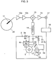
- FIG. 3 A block diagram of a low-noise converter for receiving satellite signal in embodiment 5 of the invention is shown in Fig. 3.
- a satellite signal received by a receiving antenna is led into a circular waveguide 20, converted into MSL mode by a probe 11 provided in the guide, and amplified by a low-noise amplifier, and sent into a mixer 13 to be converted down to an intermediate frequency.
- the output signal of the microwave oscillator of embodiment 1 is supplied from the dc blocking capacitor 7a into the mixer 13 through a band-pass filter 14 formed of MSL, and the bias supply terminal 2 of the transistor 1 is connected to a stabilized dc power supply circuit 16.
- the satellite signal and local oscillation signal are mixed, and the IF component is taken out from the output port of the mixer 13, amplified in an IF amplifier 15, and led to an IF output terminal 17 and delivered outside.
- the dc voltage to be supplied to the stabilized dc power supply circuit is superposed on the IF output signal from outside, and is applied from the output terminal 17.
- the microwave oscillator in embodiment 1 is used in the low-noise converter for receiving satellite signal as the local oscillator, a small and stable low-noise converter for receiving satellite signal having excellent phase noise characteristics is realized.
- a block diagram of a low-noise converter of this embodiment is same as that of embodiment 5 shown in Fig. 3.
- the microwave oscillator in embodiment 2 is used in the low-noise converter for receiving satellite signal as the local oscillator, a small and stable low-noise converter for receiving satellite signal having excellent phase noise characteristics is realized.
- FIG. 4 A block diagram of a low-noise converter for receiving satellite signal in embodiment 7 of the invention is shown in Fig. 4.
- a satellite signal received by a receiving antenna is led into a circular waveguide 20, converted into MSL mode by a probe 11 provided in the guide, and amplified by a low-noise amplifier, and sent into a mixer 13 to be converted down to an intermediate frequency.
- the output signal of the microwave oscillator of embodiment 3 is supplied from the dc blocking capacitor 7a into the mixer 13 through a band-pass filter 14 formed of MSL, and the bias supply terminal 2 of the FET 9 is connected to a stabilized dc power supply circuit 16.
- the satellite signal and local oscillation signal are mixed, and the IF component is taken out from the output port of the mixer 13, amplified in an IF amplifier 15, and led to an IF output terminal 17 and delivered outside.
- the dc voltage to be supplied to the stabilized dc power supply circuit is superposed on the IF output signal from outside, and is applied from the output terminal 17.
- the microwave oscillator in embodiment 3 is used in the low-noise converter for receiving satellite signal as the local oscillator, a small and stable low-noise converter for receiving satellite signal having excellent phase noise characteristics is realized.
- a block diagram of a low-noise converter of this embodiment is same as that of embodiment 7 shown in Fig. 4.
- the microwave oscillator in embodiment 4 since the microwave oscillator in embodiment 4 is used in the low-noise converter for receiving satellite signal as the local oscillator, a small and stable low-noise converter for receiving satellite signal having excellent phase noise characteristics is realized.
Landscapes
- Inductance-Capacitance Distribution Constants And Capacitance-Resistance Oscillators (AREA)
- Superheterodyne Receivers (AREA)
- Input Circuits Of Receivers And Coupling Of Receivers And Audio Equipment (AREA)
Abstract
Description
Claims (8)
- A microwave oscillator for inducing parallel feedback from collector to a base of a bipolar transistor, comprising:wherein λg1 is a guide wavelength of the first microstrip line at an oscillation frequency of said microwave oscillator.(a) a first microstrip line with a released end coupled to said base terminal,(b) a second microstrip line with a released end coupled to said collector terminal,(c) a dielectric resonator electromagnetically coupled to said first microstrip line and said second microstrip line, and(d) a high impedance line for bias supply to said base terminal coupled at a position where a distance from the released end on said first microstrip line to a point closest to a center of said dielectric resonator is λg1/4,
- A microwave oscillator for inducing parallel feedback from a collector to a base of a bipolar transistor, comprising:wherein λg1 and λg2 are a guide wavelengths of the first microstrip line and the second microstrip line respectively at the oscillation frequency of said microwave oscillator.(a) a first microstrip line with a released end coupled to said base terminal,(b) a second microstrip line with a released end coupled to said collector terminal,(c) a dielectric resonator electromagnetically coupled to said first microstrip line and said second microstrip line,(d) a high impedance line for bias supply to said base terminal coupled at a position where a distance from the released end on said first microstrip line to a point closest to a center of said dielectric resonator is λg1/4, and(e) a high impedance line for bias supply to said collector terminal coupled at a position where the distance from the released end on said second microstrip line to the point closest to the center of said dielectric resonator is λg2/4,
- A microwave oscillator for inducing parallel feedback from a drain to a gate of a field effect transistor, comprising:wherein λg1 is a guide wavelength of the first microstrip line at an oscillation frequency of said microwave oscillator.(a) a first microstrip line with a released end coupled to said gate terminal,(b) a second microstrip line with a released end coupled to said drain terminal,(c) a dielectric resonator electromagnetically coupled to said first microstrip line and said second microstrip line, and(d) a high impedance line for bias supply to said gate terminal coupled at a position where a distance from the released end on said first microstrip line to a point closest to a center of said dielectric resonator is λg1/4,
- A microwave oscillator for inducing parallel feedback from a drain to a gate of a field effect transistor, comprising:wherein λg1 and λg2 are a guide wavelengths of the first microstrip line and the second microstrip line respectively at the oscillation frequency of said microwave oscillator.(a) a first microstrip line with a released end coupled to said gate terminal,(b) a second microstrip line with a released end coupled to said drain terminal,(c) a dielectric resonator electromagnetically coupled to said first microstrip line and said second microstrip line,(d) a high impedance line for bias supply to said gate terminal coupled at a position where a distance from the released end on said first microstrip line to a point closest to a center of said dielectric resonator is λg1/4, and(e) a high impedance line for bias supply to said drain terminal coupled at a position where the distance from the released end on said second microstrip line to the point closest to the center of said dielectric resonator is λg2/4,
- A low-noise converter incorporated in a microwave receiving antenna comprising:wherein said local oscillator includes the microwave oscillator of claim 1.(a) a waveguide for transmitting a satellite signal received in said receiving antenna,(b) a waveguide probe for converting the satellite signal in said waveguide into a microstrip line mode,(c) a low-noise amplifier of which input port is coupled to said waveguide probe,(d) a mixer for receiving an output signal of said low-noise amplifier, and(e) a local oscillator of which output port is coupled to said mixer,
- A low-noise converter incorporated in a microwave receiving antenna comprising:wherein said local oscillator includes the microwave oscillator of claim 2.(a) a waveguide for transmitting a satellite signal received in said receiving antenna,(b) a waveguide probe for converting the satellite signal in said waveguide into a microstrip line mode,(c) a low-noise amplifier of which input port is coupled to said waveguide probe,(d) a mixer for receiving the output signal of said low-noise amplifier, and(e) a local oscillator of which output port is coupled to said mixer,
- A low-noise converter incorporated in a microwave receiving antenna comprising:wherein said local oscillator includes the microwave oscillator of claim 3.(a) a waveguide for transmitting a satellite signal received in said receiving antenna,(b) a waveguide probe for converting the satellite signal in said waveguide into a microstrip line mode,(c) a low-noise amplifier of which input port is coupled to said waveguide probe,(d) a mixer for receiving the output signal of said low-noise amplifier, and(e) a local oscillator of which output port is coupled to said mixer,
- A low-noise converter incorporated in a microwave receiving antenna comprising:wherein said local oscillator includes the microwave oscillator of claim 4.(a) a waveguide for transmitting a satellite signal received in said receiving antenna,(b) a waveguide probe for converting the satellite signal in said waveguide into a microstrip line mode,(c) a low-noise amplifier of which input port is coupled to said waveguide probe,(d) a mixer for receiving the output signal of said low-noise amplifier, and(e) a local oscillator of which output port is coupled to said mixer,
Applications Claiming Priority (2)
| Application Number | Priority Date | Filing Date | Title |
|---|---|---|---|
| JP2000107545 | 2000-04-10 | ||
| JP2000107545A JP4378835B2 (en) | 2000-04-10 | 2000-04-10 | Microwave oscillator and satellite reception downconverter |
Publications (3)
| Publication Number | Publication Date |
|---|---|
| EP1154561A2 true EP1154561A2 (en) | 2001-11-14 |
| EP1154561A3 EP1154561A3 (en) | 2002-08-21 |
| EP1154561B1 EP1154561B1 (en) | 2004-12-15 |
Family
ID=18620527
Family Applications (1)
| Application Number | Title | Priority Date | Filing Date |
|---|---|---|---|
| EP01108601A Expired - Lifetime EP1154561B1 (en) | 2000-04-10 | 2001-04-05 | Microwave oscillator and low-noise converter using the same |
Country Status (5)
| Country | Link |
|---|---|
| US (1) | US6987960B2 (en) |
| EP (1) | EP1154561B1 (en) |
| JP (1) | JP4378835B2 (en) |
| CN (1) | CN1245806C (en) |
| DE (1) | DE60107751T2 (en) |
Families Citing this family (5)
| Publication number | Priority date | Publication date | Assignee | Title |
|---|---|---|---|---|
| DE602004010157T2 (en) * | 2003-09-18 | 2008-10-30 | Thomson Licensing | Bidirectional wide-distribution user terminal with configurable radiated frequencies |
| JP3939726B2 (en) * | 2005-02-10 | 2007-07-04 | 株式会社神戸製鋼所 | Negative resistance input amplifier circuit and oscillation circuit |
| JP4772617B2 (en) * | 2006-07-31 | 2011-09-14 | 新日本無線株式会社 | High frequency oscillator |
| CN101662263B (en) * | 2008-08-27 | 2012-11-21 | 中国科学院微电子研究所 | Bias Circuit for Matched Field Effect Transistors in Ku Band |
| CN109039286A (en) * | 2018-06-28 | 2018-12-18 | 电子科技大学中山学院 | Novel light-operated microwave oscillator |
Family Cites Families (5)
| Publication number | Priority date | Publication date | Assignee | Title |
|---|---|---|---|---|
| FR2513456A1 (en) * | 1981-09-23 | 1983-03-25 | Centre Nat Rech Scient | Multiple output ceramic dielectric transistor microwave oscillator - has two similar resonators formed on substrate using microstrip connection technique |
| JPS59224904A (en) * | 1983-06-03 | 1984-12-17 | Murata Mfg Co Ltd | Oscillating circuit |
| CN1056255C (en) * | 1993-01-30 | 2000-09-06 | 汤姆森电子消费品公司 | Converter |
| EP0683561A1 (en) * | 1994-05-18 | 1995-11-22 | Guan-Wu Wang | Low-cost low noise block down-converter with a self-oscillating mixer for satellite broadcast receivers |
| FR2750816B1 (en) * | 1996-07-03 | 1998-10-23 | Matra Marconi Space France | DIELECTRIC RESONATOR SOURCE IN GALLERY MODE |
-
2000
- 2000-04-10 JP JP2000107545A patent/JP4378835B2/en not_active Expired - Lifetime
-
2001
- 2001-04-05 DE DE60107751T patent/DE60107751T2/en not_active Expired - Fee Related
- 2001-04-05 EP EP01108601A patent/EP1154561B1/en not_active Expired - Lifetime
- 2001-04-10 US US09/829,483 patent/US6987960B2/en not_active Expired - Fee Related
- 2001-04-10 CN CNB011168382A patent/CN1245806C/en not_active Expired - Fee Related
Also Published As
| Publication number | Publication date |
|---|---|
| JP2001292029A (en) | 2001-10-19 |
| US20010055958A1 (en) | 2001-12-27 |
| US6987960B2 (en) | 2006-01-17 |
| DE60107751D1 (en) | 2005-01-20 |
| EP1154561A3 (en) | 2002-08-21 |
| CN1317883A (en) | 2001-10-17 |
| DE60107751T2 (en) | 2005-12-01 |
| CN1245806C (en) | 2006-03-15 |
| JP4378835B2 (en) | 2009-12-09 |
| EP1154561B1 (en) | 2004-12-15 |
Similar Documents
| Publication | Publication Date | Title |
|---|---|---|
| KR100196241B1 (en) | Microwave mixing circuit | |
| US7072636B2 (en) | Printed circuit doubly balanced mixer for upconverter | |
| US5939939A (en) | Power combiner with harmonic selectivity | |
| EP0683561A1 (en) | Low-cost low noise block down-converter with a self-oscillating mixer for satellite broadcast receivers | |
| US20080174375A1 (en) | Voltage-controlled oscillator and communication device using the same | |
| US4641369A (en) | Local oscillator and mixer assembly | |
| US7164902B2 (en) | Filter-integrated even-harmonic mixer and hi-frequency radio communication device using the same | |
| US4605909A (en) | Dual gate FET oscillator mixer | |
| CA1205901A (en) | Wideband if amplifier with complementary gaas fet- bipolar transistor combination | |
| US5418500A (en) | High-frequency oscillator circuit | |
| US5960334A (en) | Amplifier and portable telephone apparatus using the same | |
| US4429417A (en) | Integrated antenna, amplifier and converter for microwave frequencies | |
| US6987960B2 (en) | Microwave oscillator and low-noise converter using the same | |
| US20060105732A1 (en) | Wideband image rejection mixer | |
| US3818365A (en) | Microwave amplifier circuit utilizing negative resistance diode | |
| US4267604A (en) | UHF electronic tuner | |
| US6724274B2 (en) | Frequency-switching oscillator and electronic device using the same | |
| EP0548885A2 (en) | TDMA-TDD transmitter-receiver | |
| US7512394B2 (en) | Wideband up-conversion mixer | |
| JP3929254B2 (en) | High frequency circuit and communication device using the same | |
| JP2002217727A (en) | Injection-locked oscillator, oscillator, and high-frequency communication device using them | |
| EP0247749A2 (en) | Push-push dielectric resonator oscillator | |
| US6675005B2 (en) | Printed single balanced downconverter mixer | |
| JPH02128506A (en) | Oscillation mixing circuit | |
| US6369664B1 (en) | Voltage controlled oscillator and electronic apparatus using same |
Legal Events
| Date | Code | Title | Description |
|---|---|---|---|
| PUAI | Public reference made under article 153(3) epc to a published international application that has entered the european phase |
Free format text: ORIGINAL CODE: 0009012 |
|
| AK | Designated contracting states |
Kind code of ref document: A2 Designated state(s): AT BE CH CY DE DK ES FI FR GB GR IE IT LI LU MC NL PT SE TR |
|
| AX | Request for extension of the european patent |
Free format text: AL;LT;LV;MK;RO;SI |
|
| PUAL | Search report despatched |
Free format text: ORIGINAL CODE: 0009013 |
|
| AK | Designated contracting states |
Kind code of ref document: A3 Designated state(s): AT BE CH CY DE DK ES FI FR GB GR IE IT LI LU MC NL PT SE TR |
|
| AX | Request for extension of the european patent |
Free format text: AL;LT;LV;MK;RO;SI |
|
| RIC1 | Information provided on ipc code assigned before grant |
Free format text: 7H 03B 5/18 A, 7H 03D 7/00 B |
|
| 17P | Request for examination filed |
Effective date: 20020923 |
|
| 17Q | First examination report despatched |
Effective date: 20030220 |
|
| AKX | Designation fees paid |
Designated state(s): DE FR GB |
|
| GRAP | Despatch of communication of intention to grant a patent |
Free format text: ORIGINAL CODE: EPIDOSNIGR1 |
|
| GRAS | Grant fee paid |
Free format text: ORIGINAL CODE: EPIDOSNIGR3 |
|
| GRAA | (expected) grant |
Free format text: ORIGINAL CODE: 0009210 |
|
| AK | Designated contracting states |
Kind code of ref document: B1 Designated state(s): DE FR GB |
|
| REG | Reference to a national code |
Ref country code: GB Ref legal event code: FG4D |
|
| REG | Reference to a national code |
Ref country code: IE Ref legal event code: FG4D |
|
| REF | Corresponds to: |
Ref document number: 60107751 Country of ref document: DE Date of ref document: 20050120 Kind code of ref document: P |
|
| ET | Fr: translation filed | ||
| PLBE | No opposition filed within time limit |
Free format text: ORIGINAL CODE: 0009261 |
|
| STAA | Information on the status of an ep patent application or granted ep patent |
Free format text: STATUS: NO OPPOSITION FILED WITHIN TIME LIMIT |
|
| 26N | No opposition filed |
Effective date: 20050916 |
|
| PGFP | Annual fee paid to national office [announced via postgrant information from national office to epo] |
Ref country code: DE Payment date: 20090402 Year of fee payment: 9 Ref country code: FR Payment date: 20090417 Year of fee payment: 9 |
|
| PGFP | Annual fee paid to national office [announced via postgrant information from national office to epo] |
Ref country code: GB Payment date: 20090401 Year of fee payment: 9 |
|
| GBPC | Gb: european patent ceased through non-payment of renewal fee |
Effective date: 20100405 |
|
| REG | Reference to a national code |
Ref country code: FR Ref legal event code: ST Effective date: 20101230 |
|
| PG25 | Lapsed in a contracting state [announced via postgrant information from national office to epo] |
Ref country code: DE Free format text: LAPSE BECAUSE OF NON-PAYMENT OF DUE FEES Effective date: 20101103 |
|
| PG25 | Lapsed in a contracting state [announced via postgrant information from national office to epo] |
Ref country code: GB Free format text: LAPSE BECAUSE OF NON-PAYMENT OF DUE FEES Effective date: 20100405 |
|
| PG25 | Lapsed in a contracting state [announced via postgrant information from national office to epo] |
Ref country code: FR Free format text: LAPSE BECAUSE OF NON-PAYMENT OF DUE FEES Effective date: 20100430 |