EP1153279B1 - Solid state rf oscillator-detector for flow cytometer - Google Patents
Solid state rf oscillator-detector for flow cytometer Download PDFInfo
- Publication number
- EP1153279B1 EP1153279B1 EP00907121A EP00907121A EP1153279B1 EP 1153279 B1 EP1153279 B1 EP 1153279B1 EP 00907121 A EP00907121 A EP 00907121A EP 00907121 A EP00907121 A EP 00907121A EP 1153279 B1 EP1153279 B1 EP 1153279B1
- Authority
- EP
- European Patent Office
- Prior art keywords
- oscillator
- circuit
- detector
- coupled
- measurement cell
- Prior art date
- Legal status (The legal status is an assumption and is not a legal conclusion. Google has not performed a legal analysis and makes no representation as to the accuracy of the status listed.)
- Expired - Lifetime
Links
- 239000007787 solid Substances 0.000 title description 7
- 239000002245 particle Substances 0.000 claims description 62
- 239000003990 capacitor Substances 0.000 claims description 48
- 230000008859 change Effects 0.000 claims description 48
- 238000005259 measurement Methods 0.000 claims description 36
- 238000004804 winding Methods 0.000 claims description 36
- 238000001514 detection method Methods 0.000 claims description 21
- 230000005684 electric field Effects 0.000 claims description 11
- 230000008878 coupling Effects 0.000 claims description 9
- 238000010168 coupling process Methods 0.000 claims description 9
- 238000005859 coupling reaction Methods 0.000 claims description 9
- 230000005669 field effect Effects 0.000 claims description 9
- 238000000034 method Methods 0.000 claims description 9
- 239000008186 active pharmaceutical agent Substances 0.000 claims description 8
- 239000012530 fluid Substances 0.000 claims description 7
- 230000010355 oscillation Effects 0.000 claims description 5
- 239000011521 glass Substances 0.000 claims description 2
- 230000004048 modification Effects 0.000 claims 3
- 238000012986 modification Methods 0.000 claims 3
- 210000004027 cell Anatomy 0.000 description 82
- 230000006870 function Effects 0.000 description 10
- 230000035945 sensitivity Effects 0.000 description 9
- 238000013461 design Methods 0.000 description 7
- 230000003321 amplification Effects 0.000 description 5
- 210000000601 blood cell Anatomy 0.000 description 5
- 238000003199 nucleic acid amplification method Methods 0.000 description 5
- 230000004044 response Effects 0.000 description 5
- 210000004369 blood Anatomy 0.000 description 4
- 239000008280 blood Substances 0.000 description 4
- 230000009977 dual effect Effects 0.000 description 4
- 230000000694 effects Effects 0.000 description 4
- 230000001939 inductive effect Effects 0.000 description 4
- 230000008569 process Effects 0.000 description 4
- 230000009467 reduction Effects 0.000 description 4
- 229910000859 α-Fe Inorganic materials 0.000 description 4
- 230000000903 blocking effect Effects 0.000 description 3
- 230000001965 increasing effect Effects 0.000 description 3
- 238000002347 injection Methods 0.000 description 3
- 239000007924 injection Substances 0.000 description 3
- 229920006395 saturated elastomer Polymers 0.000 description 3
- 238000013459 approach Methods 0.000 description 2
- 230000005540 biological transmission Effects 0.000 description 2
- 230000001419 dependent effect Effects 0.000 description 2
- 238000004146 energy storage Methods 0.000 description 2
- 230000006872 improvement Effects 0.000 description 2
- 238000004519 manufacturing process Methods 0.000 description 2
- 238000004088 simulation Methods 0.000 description 2
- 239000000243 solution Substances 0.000 description 2
- 238000012546 transfer Methods 0.000 description 2
- 230000001052 transient effect Effects 0.000 description 2
- FAPWRFPIFSIZLT-UHFFFAOYSA-M Sodium chloride Chemical compound [Na+].[Cl-] FAPWRFPIFSIZLT-UHFFFAOYSA-M 0.000 description 1
- 230000009471 action Effects 0.000 description 1
- 230000032683 aging Effects 0.000 description 1
- QGLZXHRNAYXIBU-WEVVVXLNSA-N aldicarb Chemical compound CNC(=O)O\N=C\C(C)(C)SC QGLZXHRNAYXIBU-WEVVVXLNSA-N 0.000 description 1
- 230000017531 blood circulation Effects 0.000 description 1
- 210000001124 body fluid Anatomy 0.000 description 1
- 239000010839 body fluid Substances 0.000 description 1
- 230000015556 catabolic process Effects 0.000 description 1
- 239000002131 composite material Substances 0.000 description 1
- 239000004020 conductor Substances 0.000 description 1
- 238000012937 correction Methods 0.000 description 1
- 125000004122 cyclic group Chemical group 0.000 description 1
- 230000007423 decrease Effects 0.000 description 1
- 238000006731 degradation reaction Methods 0.000 description 1
- 238000003745 diagnosis Methods 0.000 description 1
- 238000010586 diagram Methods 0.000 description 1
- 201000010099 disease Diseases 0.000 description 1
- 208000037265 diseases, disorders, signs and symptoms Diseases 0.000 description 1
- 238000006073 displacement reaction Methods 0.000 description 1
- 230000003116 impacting effect Effects 0.000 description 1
- 238000011835 investigation Methods 0.000 description 1
- 238000012423 maintenance Methods 0.000 description 1
- 239000000463 material Substances 0.000 description 1
- 238000012545 processing Methods 0.000 description 1
- 230000008439 repair process Effects 0.000 description 1
- 239000004065 semiconductor Substances 0.000 description 1
- 230000002277 temperature effect Effects 0.000 description 1
- 230000007704 transition Effects 0.000 description 1
Images


Classifications
-
- G—PHYSICS
- G01—MEASURING; TESTING
- G01N—INVESTIGATING OR ANALYSING MATERIALS BY DETERMINING THEIR CHEMICAL OR PHYSICAL PROPERTIES
- G01N15/00—Investigating characteristics of particles; Investigating permeability, pore-volume or surface-area of porous materials
- G01N15/10—Investigating individual particles
- G01N15/1031—Investigating individual particles by measuring electrical or magnetic effects
- G01N15/12—Investigating individual particles by measuring electrical or magnetic effects by observing changes in resistance or impedance across apertures when traversed by individual particles, e.g. by using the Coulter principle
- G01N15/131—Details
- G01N15/132—Circuits
-
- H—ELECTRICITY
- H03—ELECTRONIC CIRCUITRY
- H03B—GENERATION OF OSCILLATIONS, DIRECTLY OR BY FREQUENCY-CHANGING, BY CIRCUITS EMPLOYING ACTIVE ELEMENTS WHICH OPERATE IN A NON-SWITCHING MANNER; GENERATION OF NOISE BY SUCH CIRCUITS
- H03B5/00—Generation of oscillations using amplifier with regenerative feedback from output to input
- H03B5/08—Generation of oscillations using amplifier with regenerative feedback from output to input with frequency-determining element comprising lumped inductance and capacitance
- H03B5/12—Generation of oscillations using amplifier with regenerative feedback from output to input with frequency-determining element comprising lumped inductance and capacitance active element in amplifier being semiconductor device
- H03B5/1206—Generation of oscillations using amplifier with regenerative feedback from output to input with frequency-determining element comprising lumped inductance and capacitance active element in amplifier being semiconductor device using multiple transistors for amplification
- H03B5/1218—Generation of oscillations using amplifier with regenerative feedback from output to input with frequency-determining element comprising lumped inductance and capacitance active element in amplifier being semiconductor device using multiple transistors for amplification the generator being of the balanced type
-
- H—ELECTRICITY
- H03—ELECTRONIC CIRCUITRY
- H03B—GENERATION OF OSCILLATIONS, DIRECTLY OR BY FREQUENCY-CHANGING, BY CIRCUITS EMPLOYING ACTIVE ELEMENTS WHICH OPERATE IN A NON-SWITCHING MANNER; GENERATION OF NOISE BY SUCH CIRCUITS
- H03B5/00—Generation of oscillations using amplifier with regenerative feedback from output to input
- H03B5/08—Generation of oscillations using amplifier with regenerative feedback from output to input with frequency-determining element comprising lumped inductance and capacitance
- H03B5/12—Generation of oscillations using amplifier with regenerative feedback from output to input with frequency-determining element comprising lumped inductance and capacitance active element in amplifier being semiconductor device
- H03B5/1228—Generation of oscillations using amplifier with regenerative feedback from output to input with frequency-determining element comprising lumped inductance and capacitance active element in amplifier being semiconductor device the amplifier comprising one or more field effect transistors
-
- H—ELECTRICITY
- H03—ELECTRONIC CIRCUITRY
- H03B—GENERATION OF OSCILLATIONS, DIRECTLY OR BY FREQUENCY-CHANGING, BY CIRCUITS EMPLOYING ACTIVE ELEMENTS WHICH OPERATE IN A NON-SWITCHING MANNER; GENERATION OF NOISE BY SUCH CIRCUITS
- H03B5/00—Generation of oscillations using amplifier with regenerative feedback from output to input
- H03B5/08—Generation of oscillations using amplifier with regenerative feedback from output to input with frequency-determining element comprising lumped inductance and capacitance
- H03B5/12—Generation of oscillations using amplifier with regenerative feedback from output to input with frequency-determining element comprising lumped inductance and capacitance active element in amplifier being semiconductor device
- H03B5/1237—Generation of oscillations using amplifier with regenerative feedback from output to input with frequency-determining element comprising lumped inductance and capacitance active element in amplifier being semiconductor device comprising means for varying the frequency of the generator
- H03B5/124—Generation of oscillations using amplifier with regenerative feedback from output to input with frequency-determining element comprising lumped inductance and capacitance active element in amplifier being semiconductor device comprising means for varying the frequency of the generator the means comprising a voltage dependent capacitance
-
- H—ELECTRICITY
- H03—ELECTRONIC CIRCUITRY
- H03B—GENERATION OF OSCILLATIONS, DIRECTLY OR BY FREQUENCY-CHANGING, BY CIRCUITS EMPLOYING ACTIVE ELEMENTS WHICH OPERATE IN A NON-SWITCHING MANNER; GENERATION OF NOISE BY SUCH CIRCUITS
- H03B5/00—Generation of oscillations using amplifier with regenerative feedback from output to input
- H03B5/08—Generation of oscillations using amplifier with regenerative feedback from output to input with frequency-determining element comprising lumped inductance and capacitance
- H03B5/12—Generation of oscillations using amplifier with regenerative feedback from output to input with frequency-determining element comprising lumped inductance and capacitance active element in amplifier being semiconductor device
- H03B5/1296—Generation of oscillations using amplifier with regenerative feedback from output to input with frequency-determining element comprising lumped inductance and capacitance active element in amplifier being semiconductor device the feedback circuit comprising a transformer
Definitions
- the present invention relates in general to RF oscillator/detectors of the type that are used for conducting electrical measurements of particles (e.g., blood cells) contained in a carrier fluid in a flow cytometer system.
- the invention is particularly directed to a new and improved solid state RF oscillator-detector circuit, that employs a dual junction field effect transistor (JFET)-based Hartley RF oscillator, having a relatively low Q tank circuit, that is coupled to the flow cell by an impedance-matching transformer.
- JFET junction field effect transistor
- a patient's body fluid e.g., blood cells
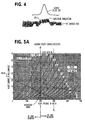
- particle flow cytometers such as that diagrammatically illustrated at 10 in Figure 1
- a whole blood sample is initially diluted with a saline solution, lysed to explode all the red cells, and then stabilized to return the remaining white cells to their original size.
- the prepared blood sample is then placed in a sample holding chamber 12, and a stream of the blood sample is conveyed along a flow channel 11 from the holding chamber 12 through a restricted orifice or aperture 14, that allows particles to be counted one at the time, and into a receiving chamber 16.
- a DC electrical field for measuring the displaced volume of each particle and an RF field for measuring the density of each particle passing through the aperture 14 are applied to the flow cell 10 by way of an oscillator-detector circuit 17, which is preferably configured as a Hartley oscillator (although other oscillator architectures may also be used).
- a tube-based flow cell measurement circuit of the type shown in Figure 1 is effective to provide an indication of both particle size and density, it suffers from a number of problems which are both costly and time-consuming to remedy.
- a fundamental shortcoming is the fact that it was originally designed as and continues to be configured using relatively old electronic tube components. This potentially impacts component availability, as the number of manufacturers of vacuum (as well as gas filled) electronic tubes continues to decline.
- the effective lifetime of a newly purchased and installed tube in the RF (Hartley) oscillator is not only unpredictable, but experience has shown that the effective functionality of most tubes within the Hartley oscillator - detector circuit is very limited, (even though a tube tester transconductance measurement shows a tube to be good). At best a tube can expect to last somewhere in a range of three to nine months - and typically involves on the order of two repair/maintenance service calls per year per flow cell.
- a RF oscillator-detector circuit suitable for use in an apparatus for conducting electrical measurements of particles contained in a carrier fluid passing through an aperture in a measurement cell to which an electric field is applied, is defined in claim 1.
- apparatus for conducting electrical measurements of particles contained in the carrier fluid passing through an aperture in a measurement cell is defined in claim 8.
- a method of coupling a RF field to a measurement cell in an apparatus for conducting electrical measurements of particles contained in a carrier fluid passing through an aperture in said measurement cell, to which an electric field is applied is defined in claim 9.
- JFETs are inherently noiseless, except for the thermal noise intrinsic with channel resistance between the drain and the source.
- the oscillator/detector In the operation of the oscillator/detector, it is very easy to be misled as to the value of rms noise level seen at the detector output.
- the circuit noise that is coupled to the detector output is primarily related to the conduction time of JFET channel resistance. The shorter conduction time, reduction of channel resistance, or reduction of channel current, the lower the effective noise.
- a pair of parallel-coupled JFETs having different transfer functions, in particular different pinchoff V GS and max I DSS characteristics, are employed as the principal active element of the RF oscillator.
- transfer functions in particular different pinchoff V GS and max I DSS characteristics.
- both devices are operated in their linear saturated regions with the RF load lines.
- both devices operate in their square-law regions, as shown in the pulse load line. This is not intuitively evident from a circuit simulation, as only the RF region is operative and the simulation models do not include the square-law region. Operation in the saturation region cannot develop any detectable change due to a perturbation in the loading by a cell.
- each device With a pair of JFETs operating with different parameters, each device will be set at a different temperature, which leads to problems with temperature stability. While it may be possible to selected two JFET devices such that they will cancel out each other's temperature curves, this is not a viable solution from a manufacturing perspective. As a result, it is preferred to install the two JFETs and an associated current mirror in a temperature control chamber. This provides the circuit designer with considerable latitude in the choice of JFETs, as only the detection process needs to be considered.
- the respective parallel-connected source-drain paths of the two (Class C, Class AB) JFETs are coupled between a DC voltage supply node and a center tap of a primary winding of a flow cell impedance-matching, ferrite core toroid transformer.
- This transformer also forms an inductive component portion of a relatively low Q resonator circuit that sets the fundamental resonant RF frequency of the oscillator.
- the frequency of the low Q tank circuit can be adjusted by a variable capacitor.
- the transformer's primary winding is coupled to parallel connected gates of the JFETs through a gate input circuit, that includes a DC battery (resistor-capacitor) path for increasing gain as a bootstrap impedance feedback at low frequencies, and a parallel capacitor path that effectively bypasses the battery at RF frequencies.
- a gate input circuit that includes a DC battery (resistor-capacitor) path for increasing gain as a bootstrap impedance feedback at low frequencies, and a parallel capacitor path that effectively bypasses the battery at RF frequencies.
- the transformer allows the required gate biasing resistance to be matched to the load presented by the flowcell.
- matching to the flow cell load is meant that the low Q tank circuit's transformer is power-matching the RF oscillator to the flow cell for optimum detection sensitivity. This is not meant to imply that the impedance of the flow cell is being matched to that of the RF oscillator.
- the grid bias resistance can be very high, for example on the order of one megohm, which allows two things to occur. First, the grid bias resistance has no loading impact on the tank circuit. Secondly, the tank circuit can have a very high Q (e.g., on the order of 120).
- the tank Q must be low (e.g., between 8 and 20), as gate resistance dominates the loading, and a step-up secondary winding provides matching between the lower impedance of the JFETs and the higher impedance of the flow cell.
- the RF voltage applied across the flow cell can be'considerably higher than could be tolerated by the JFETs directly.
- the RF voltage presented across the flow cell itself is approximately what is seen at the JFETs gates.
- an AC voltage divider is formed between the transformer secondary winding and the flow. cell with a capacitor.
- the capacitor forms part of the impedance matching between the flow cell, a coaxial feed to the flow cell, and the RF oscillator. Since a DC current is also presented to the flow cell to measure the volumetric displacement of a particle, the secondary winding of the transformer is AC-coupled to the flow cell.
- the capacitor serves to match the Rf oscillator to the flow cell and its coaxial feed, while blocking the DC current of the volumetric measurement.
- the primary winding of the low Q tank circuit's transformer is further coupled to a current sink compliance voltage load sensing node of a current (sink) mirror circuit.
- the current mirror circuit is operative to cause the RF oscillator to function as a load detector, by multiplying current variations by a synthetic high resistance, and is configured to maintain'a constant output impedance throughout changes in compliance voltage.
- the slope of the collector current vs. base voltage characteristics of its two bipolar transistors is relatively shallow, so that with load changes the output impedance will remain effectively constant and high.
- the current mirror is coupled to a bypass capacitor which provides both a low impedance path to ground for the RF signal, and serves as an energy storage device for ensuring a good transient response for the current mirror circuit.
- the bypass capacitor serves to capture a change in RF oscillator load due to a particle passing through the flow cell aperture.
- the value of the bypass capacitor is chosen to match the RF impedance seen looking into the tank transformer. Thus, the value of the capacitor will have the same RF impedance as that of the tank winding. This matching of the RF impedances will yield the maximum detected load change signal.
- the RF oscillator employs both a Class C JFET and a Class AB JFET.
- Class C the conduction angle is 153 degrees.
- Class AB causes the conduction angle to be increased to a value between 200 and 300 degrees. Since there is no steady state conduction of either JFET, the JFETs may be considered to be operating as current pumps rather than as linear devices.
- Each JFET injects a current pulse simultaneously with the cyclic swing of the tank circuit.
- the Class AB JFET has a higher pinchoff voltage and lower max Idss than the Class C JFET. As a consequence, the Class AB JFET injects a smaller current pulse but of longer duration into the tank circuit than the Class C JFET.
- the Class C JFET injects a power pulse that rapidly ramps up the gain of the loop much higher than the other JFET could achieve. Since noise is a function of current and time into an impedance, then if the power pulse is shorter than the average, the amount of noise energy is reduced. What is effectively achieved is a tradeoff between that required to sustain operation as an RF oscillator and what is required to function as a load change detector. The change in pulse current is coupled to downstream amplification circuitry.
- a DC current source delivers a prescribed current coupled by the flow cell interface circuit to a flow cell electrode, to produce a DC electrical field for measuring the size of each particle passing through the flow cell's detection aperture.
- a disturbance in this DC electric field due to a particle is reflected by a change in compliance voltage of the current source.
- the aperture resistance will also increase, increasing the current source compliance voltage, as the RF oscillator requires less current pulse injection to maintain RF amplitude.
- the nominal RF frequency is coupled by the transformer secondary through the interface circuit to the flow cell. The presence of a particle in the flow cell aperture causes a change in flow cell reactance, as the resistance and capacitance of the aperture are effectively part of the resonant circuit.
- the Q of the transformer-configured tank circuit will increase slightly due to the presence of a particle in the aperture, this does not have nearly the impact on the JFET oscillator's operation as in a tube design.
- the presence of a particle causes the oscillator's frequency to shift upwards towards the Q peak of the tank. The closer the oscillator frequency approaches that of the Q peak, the less pulse injection current is required to maintain the oscillator's voltage amplitude.
- FIG. 3 an embodiment of a dual JFET-based oscillator-detector for use in a flow cell measurement circuit in accordance with an embodiment of the present invention is schematically illustrated as comprising a solid state RF oscillator 30, that is coupled through an interface circuit 180 to a flow cell, such as a blood flow cell, shown at 10.
- a flow cell such as a blood flow cell
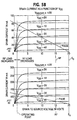
- a pair of parallel-coupled JFETs 50 and 60 having respectively different transfer functions, in particular different pinchoff V GS and max I DSS characteristics, such as those shown'in Figure 5B, are employed as the principal active elements of the RF oscillator 30.
- the two JFETs 50 and 60 are operated in their linear saturated regions with their RF load lines of Figure 5B.
- the load change is observed as the average in the compliance voltage across a by-pass capacitor 170 of a current (sink) mirror circuit 150.
- a first JFET (e.g., JFET 50) operates in Class C mode, while a second JFET (JFET 60) operates in Class AB mode.
- JFET 50 operates in Class C mode
- JFET 60 operates in Class AB mode.
- V GS first V GS
- V GS60 second V GS
- the net effect is a slope change in the composite V DS vs. I DS characteristic when the class C device (e.g., JFET 60) turns on (when V GS reaches 4v).
- JFETs operating in a V GS range of (-1 to -7) volts, such as J111 Series JFETS from TEMIC Semiconductor, or 2N6550 JFETS from InterFET may be employed.
- V GS and I DS are preferably enclosed in a temperature controlled housing or chamber.
- a temperature controlled environment provides the circuit designer with considerable freedom to choose JFET characteristics that provide the intended detector performance. In effect, essentially any two JFETs having V GS values more than two volts apart can be used. The remaining design parameter is oscillator current for maximum detector sensitivity.
- the respective parallel source-drain paths 51-52 and 61-62 of JFETs 50 and 60 are coupled between a DC voltage supply node 32 and a first end 71 of a bias resistor 70, a second end 72 of which is coupled to a center tap node 83 of a primary winding 80 of a multiple winding transformer 90.
- the transformer 90 is preferably of a ferrite core based, toroidal winding configuration and is used to step the voltage swing of the RF oscillation voltage up to the flow cell load and increase the load impedance seen by the flow cell, namely matching the impedance of the flow cell with that of the oscillator.
- the transformer forms an inductive component portion of a relatively low Q LC tank or resonator circuit shown in dotted lines 100, that sets the fundamental resonant frequency of the RF oscillator 30.
- a multiple winding transformer also involves the following considerations. For a transformer having only two windings, three resonant frequencies are possible: 1- primary with the addition of the secondary capacitance; 2- secondary with the addition of the primary capacitance; and 3- primary with the addition of mutual capacitance. Where additional windings are involved, there is an increase in the number of possible resonant frequencies.
- LC tank circuit 100 since LC tank circuit 100 has a low Q, it has little sensitivity to reactance changes in the flow cell, as there is insignificant change in frequency. Therefore, the tank 100 responds almost exclusively to the real resistance change caused by the loading of a particle. This contributes to JFET detector 30 responding only to resistance loading changes caused by the particle, resulting in better small particle linearity.
- a first end node 81 of primary winding 80 is coupled to a first end 111 of a fixed value capacitor 110.
- a second end 112 of capacitor 110 is coupled to the center tap node 83 of primary winding 80.
- the end node 82 serves as a current sink compliance voltage load sensing node of a current mirror circuit 150, and is coupled to a first end 121 of a variable capacitor 120.
- a second end 122 of capacitor 120 is coupled to end node 81 of primary winding 80.
- the average DC voltage at node 82 reflects a change in loading of the Rf oscillator by a particle.
- the combined capacitance of capacitors 110 and 120 and the inductance of the primary winding 80 and a secondary winding 130 of the tank/resonator circuit 100 are selected to establish the resonant frequency of the oscillator, for example, in a range of from 10 - 40 MHz, as a non-limiting example.
- the value of the capacitor 110 is preferably selected to stabilize the frequency of operation of the RF oscillator 30 (prevent hopping between resonant frequencies associated with the two transformer windings, as described).
- the use of variable capacitor 120 allows the resonant frequency to be 'tuned' as desired within the available range defined by the parameters of the tank circuit's LC components.
- variable tuning capacitor 120 may comprise a glass piston tuning capacitor. This type of capacitor serves to prevent changes in capacitor value as a result of changes in atmospheric pressure, and thereby eliminates the issue of manufacturing the circuit at sea level for use at an elevated altitude.
- the first end node 81 of the primary winding 80 is further coupled to the parallel connected gates 53 and 63 of JFETs 50 and 60, through a gate input circuit 140.
- the gate input circuit 140 has a first path comprised of a capacitor 141, and a second path containing series-connected capacitor 142 and resistor 143 coupled in parallel with capacitor 141.
- the series connection second path through capacitor 142 and resistor 143 acts as a DC battery input to the gates of the JFETs 50 and 60, and also increases the gain as a bootstrap impedance feedback at low frequencies, while the first path through capacitor 141 effectively bypasses the battery at RF frequencies.
- a further gate bias resistor 144 is coupled between gates 53 and 63 and a reference potential terminal (ground).
- the values of the resistors 70 and 144 may be selected to set the particle detection sensitivity of the circuit.
- the action of the transformer 80 allows the gate bias resistor 144 to be low, without significantly loading the flow cell.
- the second end node 82 of the primary winding 80 is further coupled to a low-pass filter 40.
- Low-pass filter 40 is operative to reject the RF signal seen on a by-pass capacitor 170 within oscillator 30.
- the current mirror circuit 150 is operative to cause the oscillator 30 to function as a load detector, by multiplying current variations by a synthetic high resistance (which is equivalent to using a high voltage supply and a plate load resistor in a conventional triode tube configuration).
- the current mirror circuit 150 is configured to maintain a constant output impedance throughout changes in compliance voltage.
- the slope of the collector current vs. base voltage characteristics of the two bipolar transistors 160 and 162 should be relatively shallow, so that with load changes the output impedance will remain effectively constant and high.
- the collector 161 of the transistor 160 is coupled to the second end node 82 of the primary winding 80 and to a capacitor 170, which provides both a low impedance path to ground for the RF signal, and serves as an energy storage device for ensuring a good transient response for the current mirror circuit 150.
- Capacitor 170 serves to capture a change in RF oscillator load due to a particle passing through the flow cell aperture. As the load changes as a result of the presence of a particle in the flow cell aperture, the compliance voltage of the current mirror 150 will change.
- the values of the bypass capacitor 170 and the components of the current mirror 150 are preferably selected to maximize the magnitude of the detected RF pulse, which is sensed at the node 82, as noted above.
- the RF oscillator employs both a Class C JFET and a Class AB JFET, the current demand at the node 82 as seen by the current mirror will have only a pulse component.
- the change in pulse current is averaged across the capacitor 170 and low frequency AC coupled to downstream amplification circuitry through low-pass filter circuit 40.
- the low-pass.filter circuit 40 includes a series circuit of an inductor 42 - capacitor 43 - resistor 44 coupled to ground, with the node 45 between inductor 42 and capacitor 43 coupled to grounded capacitor 46.
- the load-induced compliance voltage such as that associated with a particle detected in the flow cell orifice, is extracted via an RF pulse output terminal 48 coupled to the node 47 between capacitor 43 and resistor 44.
- the RF output terminal 48 is ported to downstream RF pulse amplification circuitry (not shown).
- transformer 90 is used to match the impedance of the flow cell with that of the RF oscillator 30.
- transformer 90 has its secondary (toroidal) winding 130 coupled between a first port 181 of a flow cell interface circuit 180 and ground.
- the secondary winding 130 is preferably (minimal spacing) interleaved with and wound upon the same toroid core in the same winding direction as the primary winding 80 of the transformer 90, so as to provide a high coupling coefficient between the transformer windings.
- the turns ratio between the primary and secondary windings is defined in accordance with the impedance parameters of the oscillator and flow cell. As a non-limiting example the ratio of turns of the primary winding 80 to the secondary winding'130 may be 2:1.
- the flow cell interface circuit 180 is configured to couple DC and RF to and from the flow cell, while also decoupling the DC voltage from the RF signal.
- the flow cell interface circuit 180 comprises a first capacitor 190 that is coupled between the first port 181 and a second port 182.
- the first capacitor 190 of the interface circuit 180 serves as a'short circuit for RF signals, while blocking DC.
- Port 182 may be coupled to the flow cell by means of a section of transmission line, such as the center conductor 201 of a section of coaxial cable, the outer sheath 202 of which is coupled to ground.
- the use of the coupling transformer 90 to match the impedance of the flow cell to that of the RF.oscillator avoids the complexity of having to precisely set the parameters of a transmission line that could otherwise be used to connect the tank circuit to the flow cell.
- An inductor 210 is coupled between the second port 182 and a third port 183, and is employed to provide a low frequency or DC coupling and high frequency (RF-blocked) path between ports 182 and 183.
- the flow cell interface circuit 180 further includes a second capacitor 220, which is coupled between the third port 183 and a fourth port 184, which is coupled to ground. Like the first capacitor 190, the second capacitor 220 serves as a short circuit for RF signals, while blocking DC.
- the interface circuit's third port 183 is coupled via a link 230 to a DC current source 240, that contains a current mirror circuit 250 coupled between a DC power supply terminal 252 and a current supply port 241.
- Link 230 is further coupled to a DC response output port 232, that is ported to downstream DC pulse amplification circuitry (not shown).
- the transformer 90 further includes a tickler transformer winding 135 that is coupled to an input port 302 of an RF oscillation detector 300.
- RF oscillation detector 300 is comprised of a Zener diode 311 coupled in circuit between input port 302 and output port 301.
- a further Zener diode 313 and a capacitor 315 are coupled in parallel between port 301 and ground. Due to the fact that the ferrite core of transformer 90 is not functional at low frequencies, there is no low frequency noise path from the RF oscillation detector 300 into the oscillator 30.
- a high level AC voltage can be realized from only a few turns of the tickler winding 135, facilitating rectification of the signal to a DC level by the relatively simple circuit arrangement as shown.
- the current source 240 provides a prescribed DC current via port 241, which is coupled over link 230 to the third port 183 of the flow cell interface circuit 180.
- the compliance'voltage is coupled to the second port 182 and via coaxial cable 200 to one of the electrodes of the flow cell (the other electrode of which is grounded).
- the applied compliance voltage is blocked from port 181 due to the presence of capacitor 190.
- the compliance voltage is used to generate a DC electrical field for measuring the size of each particle passing through the orifice aperture of the flow cell.
- a perturbation in this DC electric field as a result of a change in resistance due to the presence of a particle is reflected by a change in the.compliance voltage on link 230, with the magnitude of the change being indicative of the volume or size of the particle.
- This particle size-representative DC pulse is applied to output port 232 for processing by downstream circuitry, as described.
- the nominal RF frequency (e.g., a 10-40 MHz signal, referenced above) generated by the RF oscillator 30 is coupled via the secondary winding 130 of the transformer 90 to the first port 181 of flow cell interface circuit 180.
- This RF signal is coupled via capacitor 190 to the second port 182 and applied via the coaxial cable 200 to one of the electrodes of the flow cell.
- the applied RF signal is blocked from port 183 due to the presence of inductor 210.
- the RF frequency produces an RF field for measuring the opacity or density of each particle passing through the orifice aperture of the flow cell.
- the presence of a particle in the flow cell aperture produces a change in reactance in the flow cell, as the resistance and capacitance of the flow cell aperture are effectively part of the resonant circuit.
- the low Q tank circuit of the invention In the low Q tank circuit of the invention, there is little change in frequency due to the presence of the particle, as there is no significant tank resonance frequency. However, the reduction in loading will still be seen and the JFETs will inject less of a current pulse into the tank circuit, to maintain the RF oscillator's amplitude. Namely, the low Q tank circuit of the invention responds almost exclusively to real resistance change caused by the loading of the particle, in contrast to a high Q tank, that is sensitive to both the real and reactive load changes, as the reactive change causes significant changes in the oscillator's frequency. Thus, the JFET detector of the invention responds only to the resistance loading changes caused by the particle, which results in better small particle linearity, which is seen mostly in particles of a diameter less than five microns.
- a change in the value of flow cell resistance will change the amplitude of the detected RF signal; and an increase in the value of the flow cell resistance will cause an increase in the oscillator's current sink compliance voltage.
- a change in the RF carrier envelope is not modulation but a baseline shift, as modulation requires a frequency or amplitude change, which a baseline shift is not.
- Class C mode JFET causes its gate-source to act as a rectifier, so that there may be some degree of modulation or waveform distortion that occurs on every particle'of the carrier. This form of waveform distortion is not considered to be modulation that is induced by the presence of a particle in the flow cell.
- the RF oscillator 30 operates principally on the real load change in the flow cell. In contrast with a tube-based oscillator circuit, frequency shift is essentially negligible, so that the detector of the invention is effectively independent of the operating frequency of the oscillator.
- the duration of the modulation of the RF current is equal to the length of time that the particle is present within the flow cell aperture.
- the peak of the RF signal can be utilized to differentiate between different particles that introduce different impedance changes to the flow cell.
- the shortcomings of a conventional tube-based flow cell measurement circuit described above are effectively obviated by the solid state-based Hartley oscillator-configured flow cell detection circuit of the invention, that not only solves the tube-aging problem, but provides substantially improved performance.
- Using a transformer as part of the low Q tank circuit not only provides the inductive component of the resonator, but matches the impedance of the load cell to the resonator.
- the inclusion of the current mirror within the RF oscillator causes the RF oscillator to function as a load detector, by multiplying current variations by a synthetic high resistance, and maintains a constant output impedance throughout changes in compliance voltage.
Landscapes
- Chemical & Material Sciences (AREA)
- Life Sciences & Earth Sciences (AREA)
- Biochemistry (AREA)
- Dispersion Chemistry (AREA)
- Physics & Mathematics (AREA)
- Health & Medical Sciences (AREA)
- Engineering & Computer Science (AREA)
- Analytical Chemistry (AREA)
- Power Engineering (AREA)
- General Health & Medical Sciences (AREA)
- General Physics & Mathematics (AREA)
- Immunology (AREA)
- Pathology (AREA)
- Measurement Of Resistance Or Impedance (AREA)
- Investigating Or Analyzing Materials By The Use Of Electric Means (AREA)
Applications Claiming Priority (5)
| Application Number | Priority Date | Filing Date | Title |
|---|---|---|---|
| US25249899A | 1999-02-18 | 1999-02-18 | |
| US252498 | 1999-02-18 | ||
| US374911 | 1999-08-13 | ||
| US09/374,911 US6323632B1 (en) | 1999-08-13 | 1999-08-13 | Solid state RF oscillator-detector for flow cytometer |
| PCT/US2000/002743 WO2000049386A2 (en) | 1999-02-18 | 2000-02-03 | Solid state rf oscillator-detector for flow cytometer |
Publications (2)
| Publication Number | Publication Date |
|---|---|
| EP1153279A2 EP1153279A2 (en) | 2001-11-14 |
| EP1153279B1 true EP1153279B1 (en) | 2004-01-07 |
Family
ID=26942369
Family Applications (1)
| Application Number | Title | Priority Date | Filing Date |
|---|---|---|---|
| EP00907121A Expired - Lifetime EP1153279B1 (en) | 1999-02-18 | 2000-02-03 | Solid state rf oscillator-detector for flow cytometer |
Country Status (4)
| Country | Link |
|---|---|
| EP (1) | EP1153279B1 (enExample) |
| JP (1) | JP4307741B2 (enExample) |
| DE (1) | DE60007617T2 (enExample) |
| WO (1) | WO2000049386A2 (enExample) |
Families Citing this family (2)
| Publication number | Priority date | Publication date | Assignee | Title |
|---|---|---|---|---|
| KR101820101B1 (ko) * | 2016-06-30 | 2018-01-18 | 서강대학교산학협력단 | 계측 장치 및 이에 사용되는 마이크로튜브의 제조 방법 |
| CN111019814B (zh) * | 2019-12-26 | 2022-12-09 | 中国科学院苏州生物医学工程技术研究所 | 一种基于纳米孔的核酸测序装置、核酸测序方法 |
Family Cites Families (4)
| Publication number | Priority date | Publication date | Assignee | Title |
|---|---|---|---|---|
| GB2011086A (en) * | 1977-10-13 | 1979-07-04 | Skf Uk Ltd | Improvements in or relating to inductive proximity detectors |
| US4785264A (en) * | 1987-05-28 | 1988-11-15 | Motorola, Inc. | Dual FET oscillator |
| US5218325A (en) * | 1992-03-31 | 1993-06-08 | Motorola, Inc. | Low noise oscillator |
| GB9215733D0 (en) * | 1992-07-24 | 1992-09-09 | British Tech Group | Method of and apparatus for determining a property of a sample |
-
2000
- 2000-02-03 EP EP00907121A patent/EP1153279B1/en not_active Expired - Lifetime
- 2000-02-03 WO PCT/US2000/002743 patent/WO2000049386A2/en not_active Ceased
- 2000-02-03 JP JP2000600078A patent/JP4307741B2/ja not_active Expired - Lifetime
- 2000-02-03 DE DE60007617T patent/DE60007617T2/de not_active Expired - Lifetime
Also Published As
| Publication number | Publication date |
|---|---|
| WO2000049386A3 (en) | 2000-12-28 |
| JP4307741B2 (ja) | 2009-08-05 |
| JP2002537556A (ja) | 2002-11-05 |
| EP1153279A2 (en) | 2001-11-14 |
| WO2000049386A2 (en) | 2000-08-24 |
| DE60007617T2 (de) | 2004-09-30 |
| DE60007617D1 (de) | 2004-02-12 |
Similar Documents
| Publication | Publication Date | Title |
|---|---|---|
| US6323632B1 (en) | Solid state RF oscillator-detector for flow cytometer | |
| Redman-White et al. | 1/f noise in passive CMOS mixers for low and zero IF integrated receivers | |
| US8330475B2 (en) | Circuit for detecting a magnitude and phase of an impedance of a load | |
| US9678182B2 (en) | System and method for processing magnetic resonance signals | |
| US7760155B2 (en) | Integrated coupler | |
| EP0601888B1 (en) | Variable gain RF amplifier with linear gain control | |
| CN106253863A (zh) | 一种功放阻抗自动调节电路及功放电路 | |
| EP1153279B1 (en) | Solid state rf oscillator-detector for flow cytometer | |
| Griffin et al. | Low-frequency NMR spectrometer | |
| Heer et al. | Floating electrometer for scanning tunneling microscope applications in the femtoampere range | |
| CN115225043B (zh) | 一种用于北斗接收机低噪声放大器的电磁防护电路 | |
| CN114966516A (zh) | 电力电压互感器谐波传输特性测试的试验系统及测试方法 | |
| Brazil et al. | Self-consistent solutions for IMPATT diode networks | |
| Pallottino et al. | A low-noise low-input conductance preamplifier for gravitational research | |
| US5418449A (en) | Device for the detection of power at the output of an electronic circuit | |
| McSpadden et al. | Diode characterization in a microstrip measurement system for high power microwave power transmission | |
| Simmons et al. | Cross modulation in transistor tuners | |
| Okean | Integrated microwave tunnel diode device | |
| Li et al. | Broadband matching of nuclear quadrupole resonance detector using non-Foster circuits | |
| Dupuis et al. | Hybrid integrated Ku-band VCO | |
| Murat et al. | Non-foster microwave circuit design for wide band active impedance matching operation | |
| KR0154598B1 (ko) | 튜너의 강입력보강회로 | |
| Galdeano et al. | SiC MOSFET turn-off overvoltage measurement | |
| Molchanov et al. | Prospect of microwave negasensors application for ecological monitoring | |
| Lahbib et al. | Design of an embedded RF signal generator for BIST application |
Legal Events
| Date | Code | Title | Description |
|---|---|---|---|
| PUAI | Public reference made under article 153(3) epc to a published international application that has entered the european phase |
Free format text: ORIGINAL CODE: 0009012 |
|
| 17P | Request for examination filed |
Effective date: 20010827 |
|
| AK | Designated contracting states |
Kind code of ref document: A2 Designated state(s): AT BE CH CY DE DK ES FI FR GB GR IE IT LI LU MC NL PT SE |
|
| 17Q | First examination report despatched |
Effective date: 20020204 |
|
| GRAH | Despatch of communication of intention to grant a patent |
Free format text: ORIGINAL CODE: EPIDOS IGRA |
|
| GRAS | Grant fee paid |
Free format text: ORIGINAL CODE: EPIDOSNIGR3 |
|
| GRAA | (expected) grant |
Free format text: ORIGINAL CODE: 0009210 |
|
| AK | Designated contracting states |
Kind code of ref document: B1 Designated state(s): DE FR GB |
|
| REG | Reference to a national code |
Ref country code: GB Ref legal event code: FG4D |
|
| REG | Reference to a national code |
Ref country code: IE Ref legal event code: FG4D |
|
| REF | Corresponds to: |
Ref document number: 60007617 Country of ref document: DE Date of ref document: 20040212 Kind code of ref document: P |
|
| ET | Fr: translation filed | ||
| PLBE | No opposition filed within time limit |
Free format text: ORIGINAL CODE: 0009261 |
|
| STAA | Information on the status of an ep patent application or granted ep patent |
Free format text: STATUS: NO OPPOSITION FILED WITHIN TIME LIMIT |
|
| REG | Reference to a national code |
Ref country code: IE Ref legal event code: MM4A |
|
| 26N | No opposition filed |
Effective date: 20041008 |
|
| REG | Reference to a national code |
Ref country code: FR Ref legal event code: PLFP Year of fee payment: 17 |
|
| REG | Reference to a national code |
Ref country code: FR Ref legal event code: PLFP Year of fee payment: 18 |
|
| REG | Reference to a national code |
Ref country code: FR Ref legal event code: PLFP Year of fee payment: 19 |
|
| PGFP | Annual fee paid to national office [announced via postgrant information from national office to epo] |
Ref country code: DE Payment date: 20190227 Year of fee payment: 20 Ref country code: GB Payment date: 20190227 Year of fee payment: 20 |
|
| PGFP | Annual fee paid to national office [announced via postgrant information from national office to epo] |
Ref country code: FR Payment date: 20190225 Year of fee payment: 20 |
|
| REG | Reference to a national code |
Ref country code: DE Ref legal event code: R071 Ref document number: 60007617 Country of ref document: DE |
|
| REG | Reference to a national code |
Ref country code: GB Ref legal event code: PE20 Expiry date: 20200202 |
|
| PG25 | Lapsed in a contracting state [announced via postgrant information from national office to epo] |
Ref country code: GB Free format text: LAPSE BECAUSE OF EXPIRATION OF PROTECTION Effective date: 20200202 |