EP1152472A2 - Image sensor pixel for global electronic shuttering - Google Patents
Image sensor pixel for global electronic shuttering Download PDFInfo
- Publication number
- EP1152472A2 EP1152472A2 EP01201381A EP01201381A EP1152472A2 EP 1152472 A2 EP1152472 A2 EP 1152472A2 EP 01201381 A EP01201381 A EP 01201381A EP 01201381 A EP01201381 A EP 01201381A EP 1152472 A2 EP1152472 A2 EP 1152472A2
- Authority
- EP
- European Patent Office
- Prior art keywords
- pixel
- pixels
- output
- transfer mechanism
- symmetry
- Prior art date
- Legal status (The legal status is an assumption and is not a legal conclusion. Google has not performed a legal analysis and makes no representation as to the accuracy of the status listed.)
- Granted
Links
Images




Classifications
-
- H—ELECTRICITY
- H04—ELECTRIC COMMUNICATION TECHNIQUE
- H04N—PICTORIAL COMMUNICATION, e.g. TELEVISION
- H04N25/00—Circuitry of solid-state image sensors [SSIS]; Control thereof
- H04N25/70—SSIS architectures; Circuits associated therewith
- H04N25/76—Addressed sensors, e.g. MOS or CMOS sensors
- H04N25/767—Horizontal readout lines, multiplexers or registers
-
- H—ELECTRICITY
- H04—ELECTRIC COMMUNICATION TECHNIQUE
- H04N—PICTORIAL COMMUNICATION, e.g. TELEVISION
- H04N25/00—Circuitry of solid-state image sensors [SSIS]; Control thereof
- H04N25/10—Circuitry of solid-state image sensors [SSIS]; Control thereof for transforming different wavelengths into image signals
- H04N25/11—Arrangement of colour filter arrays [CFA]; Filter mosaics
- H04N25/13—Arrangement of colour filter arrays [CFA]; Filter mosaics characterised by the spectral characteristics of the filter elements
- H04N25/134—Arrangement of colour filter arrays [CFA]; Filter mosaics characterised by the spectral characteristics of the filter elements based on three different wavelength filter elements
-
- H—ELECTRICITY
- H04—ELECTRIC COMMUNICATION TECHNIQUE
- H04N—PICTORIAL COMMUNICATION, e.g. TELEVISION
- H04N25/00—Circuitry of solid-state image sensors [SSIS]; Control thereof
- H04N25/10—Circuitry of solid-state image sensors [SSIS]; Control thereof for transforming different wavelengths into image signals
- H04N25/11—Arrangement of colour filter arrays [CFA]; Filter mosaics
- H04N25/13—Arrangement of colour filter arrays [CFA]; Filter mosaics characterised by the spectral characteristics of the filter elements
- H04N25/135—Arrangement of colour filter arrays [CFA]; Filter mosaics characterised by the spectral characteristics of the filter elements based on four or more different wavelength filter elements
- H04N25/136—Arrangement of colour filter arrays [CFA]; Filter mosaics characterised by the spectral characteristics of the filter elements based on four or more different wavelength filter elements using complementary colours
-
- H—ELECTRICITY
- H04—ELECTRIC COMMUNICATION TECHNIQUE
- H04N—PICTORIAL COMMUNICATION, e.g. TELEVISION
- H04N25/00—Circuitry of solid-state image sensors [SSIS]; Control thereof
- H04N25/50—Control of the SSIS exposure
-
- H—ELECTRICITY
- H04—ELECTRIC COMMUNICATION TECHNIQUE
- H04N—PICTORIAL COMMUNICATION, e.g. TELEVISION
- H04N25/00—Circuitry of solid-state image sensors [SSIS]; Control thereof
- H04N25/70—SSIS architectures; Circuits associated therewith
-
- H—ELECTRICITY
- H04—ELECTRIC COMMUNICATION TECHNIQUE
- H04N—PICTORIAL COMMUNICATION, e.g. TELEVISION
- H04N25/00—Circuitry of solid-state image sensors [SSIS]; Control thereof
- H04N25/70—SSIS architectures; Circuits associated therewith
- H04N25/76—Addressed sensors, e.g. MOS or CMOS sensors
- H04N25/78—Readout circuits for addressed sensors, e.g. output amplifiers or A/D converters
-
- H—ELECTRICITY
- H10—SEMICONDUCTOR DEVICES; ELECTRIC SOLID-STATE DEVICES NOT OTHERWISE PROVIDED FOR
- H10F—INORGANIC SEMICONDUCTOR DEVICES SENSITIVE TO INFRARED RADIATION, LIGHT, ELECTROMAGNETIC RADIATION OF SHORTER WAVELENGTH OR CORPUSCULAR RADIATION
- H10F39/00—Integrated devices, or assemblies of multiple devices, comprising at least one element covered by group H10F30/00, e.g. radiation detectors comprising photodiode arrays
- H10F39/10—Integrated devices
- H10F39/12—Image sensors
- H10F39/18—Complementary metal-oxide-semiconductor [CMOS] image sensors; Photodiode array image sensors
- H10F39/182—Colour image sensors
-
- H—ELECTRICITY
- H10—SEMICONDUCTOR DEVICES; ELECTRIC SOLID-STATE DEVICES NOT OTHERWISE PROVIDED FOR
- H10F—INORGANIC SEMICONDUCTOR DEVICES SENSITIVE TO INFRARED RADIATION, LIGHT, ELECTROMAGNETIC RADIATION OF SHORTER WAVELENGTH OR CORPUSCULAR RADIATION
- H10F39/00—Integrated devices, or assemblies of multiple devices, comprising at least one element covered by group H10F30/00, e.g. radiation detectors comprising photodiode arrays
- H10F39/80—Constructional details of image sensors
- H10F39/802—Geometry or disposition of elements in pixels, e.g. address-lines or gate electrodes
-
- H—ELECTRICITY
- H10—SEMICONDUCTOR DEVICES; ELECTRIC SOLID-STATE DEVICES NOT OTHERWISE PROVIDED FOR
- H10F—INORGANIC SEMICONDUCTOR DEVICES SENSITIVE TO INFRARED RADIATION, LIGHT, ELECTROMAGNETIC RADIATION OF SHORTER WAVELENGTH OR CORPUSCULAR RADIATION
- H10F39/00—Integrated devices, or assemblies of multiple devices, comprising at least one element covered by group H10F30/00, e.g. radiation detectors comprising photodiode arrays
- H10F39/80—Constructional details of image sensors
- H10F39/805—Coatings
- H10F39/8053—Colour filters
Definitions
- the present invention relates to the field of solid-state image sensing devices and, more specifically, to CMOS based active pixel sensors.
- CMOS active pixel image sensors have been rapidly developed to supplement and replace charge-coupled devices in many applications.
- CMOS image sensors have advantages in low-power operation as well as the higher integration capabilities for on-chip signal processing and control functions that are available with CMOS technology. Therefore, the technology is suitable for many consumer applications, including low-cost portable imaging devices.
- CMOS based sensors allow for the incorporation of numerous functions onto a single chip.
- Various prior art references have disclosed Active Pixel Sensors based on CMOS that employ sense node connected to photodetectors through transfer gates. Typically a reset gate is provided that can be used for shuttering purposes.
- CMOS sensors have been handicapped by embodiments which employ row-by-row exposure controls which allows a slit shuttering mode that is not capable of simultaneous exposure of the entire CMOS pixel array.
- An additional shutter gate is added to provide direct reset of the photodetector independent of the transfer gate.
- the addition of the gate may cause increased fixed pattern noise due to non-optimal removal rates for charges stored within the photodetectors in the prior art devices.
- the present invention addresses the shortcomings within the prior art by providing a pixel design for CMOS image sensors that has a high frame rate potential and, therefore, provides freeze-frame motion capture capabilities.
- the pixel architecture provides for a CMOS based, active pixel image sensor comprising an array of pixels formed in rows and columns, with at least a subset of the pixels having a symmetrical arrangement of a shutter gate and a transfer gate to allow for more efficient removal of electrons from the photodetector.
- the pixel architecture provides an output gate region and a shutter gate region that are symmetric about the electrostatic center of the pixel. By arranging the shutter and transfer gates, a symmetric manner about the center of the pixel, transfers of electrons to these gates are identical in both paths so that fixed pattern noise is minimized.
- a Pixel Output Bus structure also allows configurable connections to column-wise signal busses for connections to parallel output channels.
- the pixel is designed for global electronic shuttering so every pixel is exposed simultaneously to images incident upon the pixel array plane.
- This present invention is intended for use in a high frame rate image sensor that is fabricated using a Complementary Metal Oxide Semiconductor (CMOS) active pixel sensor (APS) technology and preferably incorporating a pinned photo-diode.
- CMOS Complementary Metal Oxide Semiconductor
- APS active pixel sensor
- the pixel architecture also provides a plurality of output channels formed such that each of the output channels are operatively connected to a subset of pixels wherein each of the pixels have an attribute that is the same.
- the present invention has the advantages of: (1) Allowing the accommodation of changes in the pixel output groupings for different monochrome output format or CFA patterns with only changes in metal routing layers; (2) allowing true electronic shuttering to image moving scene with all the pixels having the same capture time windows; and (3) providing a symmetric global shutter gate and transfer gate to minimize pixel-related fixed pattern noise.
- Fig. 3a is a block diagram of the high frame rate pixel design wherein a line of symmetry 80 can be drawn that, essentially, divides the pixel into two equal halves.
- a transfer gate 71 and a shutter gate 72 are formed within the pixel such that the location of the transfer gate 71 is an equal distance from the center of the pixel as the shutter gate 72.
- the placement of the shutter gate 72 and the transfer gate 71 are not only equidistant from the center of the pixel but are symmetrically placed about the line of symmetry 80. This provides for superior drainage of the electrons from the pixel which is useful in high speed devices, such as the multiple channel device of the present invention.
- the layout of the shutter gate 72 and the transfer gate 71 about the line of symmetry 80 within pixel 70 does not have to be as shown in Fig, 3a. Any pixel design that can place a shutter gate and a transfer gate such that they are equal distances from the center can essentially have a line of symmetry drawn between the shutter and transfer gates. This is very apparent with pixel design having photodetectors that are shaped in square, rectangular, circular and oval configurations.
- the Pixel Output Bus within the preferred embodiment would typically have a select transistor which connects to either one of the four column bus for channels 1, 2, 3 or 4 (81, 82, 83, 84) with only backend metal via mask layer changes by selectively making contact between the pixel output bus to one of the four column bus using one of the contacts/vias 61, 62, 63 or 64.
- the sensor can is configurable for different CFA patterns.
- Fig. 3b shows the timing for the shuttering and integration periods of the pixel 70 seen in Fig. 3a.
- the shutter gate 72 will be active prior the time ⁇ Exp in order to reset pixel 70 to a predetermined potential, which in the case of the preferred embodiment is VDD. This effectively is the shutter operation to the pixel 70.
- the signal SG to the shutter gate 72 go inactive and the integration period ⁇ INT begins.
- the transfer gate signal TG pulses transferring the photoelectrons from the pixel onto the floating diffusion 74.
- the floating diffusion 74 acts as an input to the gate of source follower transistor 76 which provides amplification that is enabled by row select transistor 78.
- the channel electronics can then be optimized for the specific attribute, for example the electronic gain is set to an optimal level. Therefore, all pixels of the same attribute are connected to one output channel using a dedicated connection matrix and the pixels having that attribute are hard-wired to the output channel of choice. That output channel then has electronics specific to the attribute being output on that output channel.
- the pixel has an output bus region which allows the determination of the final connections by changes in the metal/via/contact layers only. Therefore, the output channel assignments can be modified for different CFA patterns with minimal costs associated with metal/via/contact masking steps in the manufacturing process. This is illustrated in Figs. 2a-d and 3a-c for a four-channel implementation with either a two or a four output column bus.
- Fig. 2a is a block diagram representation of the present invention wherein image sensor 20 has parallel output channels 21, 22, 23, 24 being connected to a CFA.
- the CFA has a kernel of four pixels such as the Bayer pattern connection matrix of Fig. 1.
- the image sensor 20 illustrated in Fig. 2a has a basic difference to the prior art image sensor 9 shown in Fig. 1 in that each of the four pixels 1, 2, 3, 4 in the kernel is connected to one of the separate output channels 21, 22, 23, 24 such that all pixels 1 are connected to conductive traces 11 connecting pixels I with the output channel 21.
- Pixels 2, 3 and 4 are connected in a similar manner to output channels 22, 23, 24 through conductive traces 12, 13, and 14.
- Conductive traces 11, 12, 13, 14 connect to each of the pixels 1, 2, 3, 4 through vias 66. This connection through the vias 66 is envisioned as being one that can be hardwired when the image sensor 20 is originally manufactured, or made to be configurable in a variety of ways.
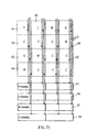
- Fig. 2b is an alternative CFA pattern where the kernel is formed as stripes of the color occupying entire rows 5, 6, 7, 8.
- the number of column busses required is increased to four.
- the vias 66 would be created to connect only two of these column busses leaving the remaining column busses unused.
- Image sensor 29 has parallel output channels 25, 26, 27, 28 being connected to a CFA of image sensor 29.
- the CFA has a kernel of four pixels arranged in rows 5, 6, 7, 8 such that each of the rows 5, 6, 7, 8 of pixels in the kernel is connected to one of the separate output channels 25, 26, 27, 28.
- Each of the pixels within the rows 5 6, 7, 8 are connected to conductive traces 31 that connect the pixels with the output channels 24, 25, 26, 27 through vias 66.
- This connection through the vias 66 is envisioned as being one that can be hardwired when the image sensor 29 is originally manufactured, or made to be configurable in a variety of ways.
- Fig. 2c illustrates that the same four column-bus arrangement shown in Fig. 2b can be "reconfigured" using minimal interconnect masking changes to allow this 4 x 4 color mosaic pattern to be wired for color-specific output channels.
- the pattern shown in Fig. 2c is a complementary color pattern having yellow color filters Y, cyan color filters C, magenta color filters M, and green color filters G.
- Each of the pixels within the pixels 41, 42, 43, 44 are connected to conductive traces 31 to output channels 45, 46, 47, 48 through vias 66.
- Fig. 2d is a similar four column-bus arrangement as shown in Figs. 2b and 2c above that is "reconfigured" for a mosaic pattern based on pixel sensitivities and with sensitivity specific output channels. As seen in Fig. 2d there are four pixel sensitivities S1, S2, S3, S4 connected to conductive traces 51 through vias 66 to output channels 45, 46, 47 and 48.
- CMOS APS In high frame rate imaging, it is also desirable to have all the pixels be exposed to a scene simultaneously with the timing controlled electronically. In a Charge-Coupled Device (CCD) image sensor, this is typically accomplished by using a vertical over-flow drain (VOD). In CMOS APS, this would add complex processing steps and therefore add cost.
- the present invention discloses the use of an additional shutter gate transistor in the pixel design to allow reset of the photo-diode collection node independently of the transfer gate and reset gate of the floating diffusion sensing node.
- this electronic shutter gate is such that the layout of the photo-diode is symmetric with respect to the two transistor gates performing either a transfer of the collected photo-carriers into a sensing node (the transfer gate) or a reset node (electronic shutter gate).
- the transfer gate performing either a transfer of the collected photo-carriers into a sensing node (the transfer gate) or a reset node (electronic shutter gate).
- the timed exposure of the pixels are determined by the time interval between the global reset of the photo-diodes and the global transfer of the photo charges to the sensing node. This design is illustrated in Figs. 3a-c.
- the present invention has advantages in: (1) accommodate changes in pixel output groupings for different monochrome output format or CFA patterns with only changes in metal routing layers; (2) allowing true electronic shuttering to image moving scene with all the pixels having the same capture time windows; and(3) providing symmetric global shutter gate and transfer gate to minimize pixel related fixed pattern noise.
Landscapes
- Engineering & Computer Science (AREA)
- Multimedia (AREA)
- Signal Processing (AREA)
- Physics & Mathematics (AREA)
- Spectroscopy & Molecular Physics (AREA)
- Solid State Image Pick-Up Elements (AREA)
- Transforming Light Signals Into Electric Signals (AREA)
- Color Television Image Signal Generators (AREA)
Abstract
Description
Claims (10)
- An image sensing device comprising:a semiconductor substrate having an array of pixels formed in two-dimensional mosaic;at least one of the pixels containing; a line of symmetry having a center, a photodetector interfaced with a sense node through a transfer mechanism, the transfer mechanism being placed on a first side of the line of symmetry within the pixel that divides the pixel into two equal parts; andan electronic shuttering mechanism placed on an opposite second side of the line of symmetry such that both the transfer mechanism and the electronic shuttering mechanism are symmetric from the center.
- The image sensing device of claim 1 where the two-dimensional mosaic of pixels is arranged in rows and columns;
- The image sensing device of claim 1 further comprising at least one active circuit element interfaced to the photodetector.
- The image sensing device of claim 1 further comprising a sense node to receive charge from the transfer mechanism and an amplifier interfaced to the sense node.
- A method of making an active pixel sensor comprising:
providing a semiconductor substrate having an array of pixels formed in rows and columns with a plurality of the pixels containing; a line of symmetry having a center, a photodetector interfaced with a sense node through a transfer mechanism, the transfer mechanism being placed on a first side of the line of symmetry within the pixel that divides the pixel into two equal parts with an electronic shuttering mechanism placed on an opposite second side of the line of symmetry within each of the plurality of pixels such that both the transfer mechanism and the electronic shuttering mechanism are equidistant and symmetric from the center and an amplifier within each of the plurality of pixels operatively connected to receive charge from the photodetector. - The method of claim 5 wherein the step of providing further comprises providing a sense node to receive charge from the transfer mechanism with the amplifier interfaced to the sense node.
- The method of claim 5 wherein the step of providing further comprises providing global shuttering means for simultaneously activating all the electronic shutters on the image sensing device.
- The method of claim 5 wherein the step of providing further comprises providing a row select transistor coupled to the amplifier.
- The method of claim 5 wherein the step of providing further comprises providing a plurality of output channels, each of the output channels being operatively connected to a subset of pixels for at least one of the columns.
- The method of claim 9 wherein the step of providing further comprises providing each of the subsets have pixels of one sensitivity.
Applications Claiming Priority (2)
| Application Number | Priority Date | Filing Date | Title |
|---|---|---|---|
| US562712 | 2000-04-28 | ||
| US09/562,712 US7129979B1 (en) | 2000-04-28 | 2000-04-28 | Image sensor pixel for global electronic shuttering |
Publications (3)
| Publication Number | Publication Date |
|---|---|
| EP1152472A2 true EP1152472A2 (en) | 2001-11-07 |
| EP1152472A3 EP1152472A3 (en) | 2005-06-08 |
| EP1152472B1 EP1152472B1 (en) | 2007-11-07 |
Family
ID=24247449
Family Applications (1)
| Application Number | Title | Priority Date | Filing Date |
|---|---|---|---|
| EP01201381A Expired - Lifetime EP1152472B1 (en) | 2000-04-28 | 2001-04-13 | Image sensor pixel layout to reduce fixed pattern noise |
Country Status (4)
| Country | Link |
|---|---|
| US (1) | US7129979B1 (en) |
| EP (1) | EP1152472B1 (en) |
| JP (1) | JP4832660B2 (en) |
| DE (1) | DE60131215T2 (en) |
Cited By (9)
| Publication number | Priority date | Publication date | Assignee | Title |
|---|---|---|---|---|
| US6847070B2 (en) | 2000-08-09 | 2005-01-25 | Dalsa, Inc. | Five transistor CMOS pixel |
| US7045753B1 (en) | 2000-08-09 | 2006-05-16 | Dalsa, Inc. | Five transistor CMOS pixel |
| EP1701536A1 (en) * | 2005-03-08 | 2006-09-13 | Sony Ericsson Mobile Communications AB | Method and device for creating pictures, using global shutter and multiple exposures |
| EP1933253A1 (en) * | 2006-12-14 | 2008-06-18 | NCR Corporation | Method, system, and apparatus for an electronic freeze frame shutter for a high pass-by image scanner |
| RU2365059C2 (en) * | 2005-03-08 | 2009-08-20 | Сони Эрикссон Мобайл Коммьюникейшнз Аб | Method and device for creation of images |
| US20140203086A1 (en) * | 2005-03-11 | 2014-07-24 | Hand Held Products, Inc. | Image reader having image sensor array |
| US9058527B2 (en) | 2005-06-03 | 2015-06-16 | Hand Held Products, Inc. | Apparatus having hybrid monochrome and color image sensor array |
| US9092654B2 (en) | 2005-06-03 | 2015-07-28 | Hand Held Products, Inc. | Digital picture taking optical reader having hybrid monochrome and color image sensor array |
| US9465970B2 (en) | 2005-03-11 | 2016-10-11 | Hand Held Products, Inc. | Image reader comprising CMOS based image sensor array |
Families Citing this family (37)
| Publication number | Priority date | Publication date | Assignee | Title |
|---|---|---|---|---|
| JP2004312107A (en) * | 2003-04-02 | 2004-11-04 | Olympus Corp | Solid-state imaging device and readout method thereof |
| KR100871687B1 (en) * | 2004-02-11 | 2008-12-05 | 삼성전자주식회사 | Solid state image pickup device with improved display quality in subsampling mode and its driving method |
| JP2005277398A (en) * | 2004-02-25 | 2005-10-06 | Sony Corp | CCD linear sensor |
| EP3905099B8 (en) * | 2005-03-11 | 2023-03-22 | Hand Held Products, Inc. | Bar code reading device with global electronic shutter control |
| DE102008009263B3 (en) * | 2008-02-15 | 2009-06-10 | Siemens Aktiengesellschaft | Motor vehicles or indicators e.g. number plate, recognition method, involves controlling light exposure in global shutter-mode to simultaneously expose all pixels of image sensor and selecting light energy that remains in permissible limit |
| US8609993B2 (en) * | 2008-05-16 | 2013-12-17 | Mitsubishi Materials Corporation | Power module substrate, power module, and method for manufacturing power module substrate |
| US7781718B2 (en) * | 2008-05-30 | 2010-08-24 | Omnivision Technologies, Inc. | Globally reset image sensor pixels |
| US8264377B2 (en) | 2009-03-02 | 2012-09-11 | Griffith Gregory M | Aircraft collision avoidance system |
| US8089036B2 (en) * | 2009-04-30 | 2012-01-03 | Omnivision Technologies, Inc. | Image sensor with global shutter and in pixel storage transistor |
| US8138531B2 (en) * | 2009-09-17 | 2012-03-20 | International Business Machines Corporation | Structures, design structures and methods of fabricating global shutter pixel sensor cells |
| KR101605984B1 (en) * | 2009-11-06 | 2016-03-23 | 가부시키가이샤 한도오따이 에네루기 켄큐쇼 | Semiconductor device |
| DE112011100842T5 (en) | 2010-03-08 | 2013-01-17 | Semiconductor Energy Laboratory Co., Ltd. | Semiconductor component and method for its production |
| JP2011239149A (en) * | 2010-05-10 | 2011-11-24 | Sony Corp | Control apparatus, camera system, and program |
| TWI429282B (en) | 2011-02-23 | 2014-03-01 | Pixart Imaging Inc | Image sensor |
| CN104270582B (en) * | 2011-03-03 | 2017-08-22 | 原相科技股份有限公司 | Image sensor with a plurality of pixels |
| CN102655572B (en) * | 2011-03-03 | 2016-06-15 | 原相科技股份有限公司 | Image Sensor |
| CN102447848B (en) * | 2012-01-17 | 2013-09-04 | 中国科学院半导体研究所 | Global shutter pixel unit of complementary metal oxide semiconductor (CMOS) image sensor |
| US9354748B2 (en) | 2012-02-13 | 2016-05-31 | Microsoft Technology Licensing, Llc | Optical stylus interaction |
| US9075566B2 (en) | 2012-03-02 | 2015-07-07 | Microsoft Technoogy Licensing, LLC | Flexible hinge spine |
| US8873227B2 (en) | 2012-03-02 | 2014-10-28 | Microsoft Corporation | Flexible hinge support layer |
| US8935774B2 (en) | 2012-03-02 | 2015-01-13 | Microsoft Corporation | Accessory device authentication |
| US9870066B2 (en) | 2012-03-02 | 2018-01-16 | Microsoft Technology Licensing, Llc | Method of manufacturing an input device |
| US9134807B2 (en) | 2012-03-02 | 2015-09-15 | Microsoft Technology Licensing, Llc | Pressure sensitive key normalization |
| US20130300590A1 (en) | 2012-05-14 | 2013-11-14 | Paul Henry Dietz | Audio Feedback |
| US8964379B2 (en) | 2012-08-20 | 2015-02-24 | Microsoft Corporation | Switchable magnetic lock |
| US8786767B2 (en) | 2012-11-02 | 2014-07-22 | Microsoft Corporation | Rapid synchronized lighting and shuttering |
| US10120420B2 (en) | 2014-03-21 | 2018-11-06 | Microsoft Technology Licensing, Llc | Lockable display and techniques enabling use of lockable displays |
| KR102170879B1 (en) | 2014-04-18 | 2020-10-29 | 삼성전자주식회사 | Image sensor and image processing system having the same |
| US10324733B2 (en) | 2014-07-30 | 2019-06-18 | Microsoft Technology Licensing, Llc | Shutdown notifications |
| US9526468B2 (en) | 2014-09-09 | 2016-12-27 | General Electric Company | Multiple frame acquisition for exposure control in X-ray medical imagers |
| US10163968B2 (en) | 2015-01-23 | 2018-12-25 | Dartmouth College | Multi-junction pixel image sensor with dielectric reflector between photodetection layers |
| US10863131B2 (en) | 2015-05-20 | 2020-12-08 | Samsung Electronics Co., Ltd. | Image sensor including parallel output of pixel signals from a pixel unit and image processing system including the same |
| US9955099B2 (en) * | 2016-06-21 | 2018-04-24 | Hand Held Products, Inc. | Minimum height CMOS image sensor |
| JP7062692B2 (en) | 2018-02-20 | 2022-05-06 | インテリジェント クリーニング イクイップメント ホールディングス カンパニー リミテッド | Tracking system, object tracking system, and related usage |
| KR20230078684A (en) * | 2020-09-03 | 2023-06-02 | 더 리서치 파운데이션 포 더 스테이트 유니버시티 오브 뉴욕 | Systems and methods for crystal-channel coupling |
| US11682313B2 (en) | 2021-03-17 | 2023-06-20 | Gregory M. Griffith | Sensor assembly for use in association with aircraft collision avoidance system and method of using the same |
| CN119788980B (en) * | 2024-11-14 | 2025-10-24 | 北京航天发射技术研究所 | A real-time processing method and device for self-collimating light tube |
Family Cites Families (17)
| Publication number | Priority date | Publication date | Assignee | Title |
|---|---|---|---|---|
| US3845295A (en) * | 1973-05-02 | 1974-10-29 | Rca Corp | Charge-coupled radiation sensing circuit with charge skim-off and reset |
| US4322638A (en) | 1980-01-16 | 1982-03-30 | Eastman Kodak Company | Image sensor adaptable for fast frame readout |
| JPH07312726A (en) * | 1994-05-19 | 1995-11-28 | Mitsubishi Electric Corp | Solid-state imaging device and driving method thereof |
| US5789774A (en) * | 1996-03-01 | 1998-08-04 | Foveonics, Inc. | Active pixel sensor cell that minimizes leakage current |
| US5631703A (en) | 1996-05-29 | 1997-05-20 | Eastman Kodak Company | Particular pattern of pixels for a color filter array which is used to derive luminance and chrominance values |
| US6173894B1 (en) * | 1996-08-23 | 2001-01-16 | Psc Inc. | Optical reader with addressable pixels |
| US5898168A (en) | 1997-06-12 | 1999-04-27 | International Business Machines Corporation | Image sensor pixel circuit |
| KR100246358B1 (en) * | 1997-09-25 | 2000-03-15 | 김영환 | Active pixel sensor with electronic shutter |
| US5952686A (en) | 1997-12-03 | 1999-09-14 | Hewlett-Packard Company | Salient integration mode active pixel sensor |
| US6046444A (en) | 1997-12-08 | 2000-04-04 | Intel Corporation | High sensitivity active pixel with electronic shutter |
| KR100266657B1 (en) * | 1998-01-20 | 2000-10-02 | 김영환 | Mos type amplifying image sensing device having double reset structure |
| US6667768B1 (en) * | 1998-02-17 | 2003-12-23 | Micron Technology, Inc. | Photodiode-type pixel for global electronic shutter and reduced lag |
| US6388241B1 (en) * | 1998-02-19 | 2002-05-14 | Photobit Corporation | Active pixel color linear sensor with line—packed pixel readout |
| US6160282A (en) * | 1998-04-21 | 2000-12-12 | Foveon, Inc. | CMOS image sensor employing silicide exclusion mask to reduce leakage and improve performance |
| US6466266B1 (en) * | 1998-07-28 | 2002-10-15 | Eastman Kodak Company | Active pixel sensor with shared row timing signals |
| US6469332B1 (en) * | 1998-09-16 | 2002-10-22 | Micron Technology, Inc. | Pinned floating photoreceptor with active pixel sensor |
| US6624850B1 (en) * | 1998-12-30 | 2003-09-23 | Eastman Kodak Company | Photogate active pixel sensor with high fill factor and correlated double sampling |
-
2000
- 2000-04-28 US US09/562,712 patent/US7129979B1/en not_active Expired - Lifetime
-
2001
- 2001-04-13 DE DE60131215T patent/DE60131215T2/en not_active Expired - Lifetime
- 2001-04-13 EP EP01201381A patent/EP1152472B1/en not_active Expired - Lifetime
- 2001-04-25 JP JP2001128321A patent/JP4832660B2/en not_active Expired - Fee Related
Cited By (42)
| Publication number | Priority date | Publication date | Assignee | Title |
|---|---|---|---|---|
| US7045753B1 (en) | 2000-08-09 | 2006-05-16 | Dalsa, Inc. | Five transistor CMOS pixel |
| US6847070B2 (en) | 2000-08-09 | 2005-01-25 | Dalsa, Inc. | Five transistor CMOS pixel |
| KR101313998B1 (en) * | 2005-03-08 | 2013-10-01 | 소니 모빌 커뮤니케이션즈 에이비 | Method and device for creating a photo |
| EP1701536A1 (en) * | 2005-03-08 | 2006-09-13 | Sony Ericsson Mobile Communications AB | Method and device for creating pictures, using global shutter and multiple exposures |
| WO2006094871A1 (en) * | 2005-03-08 | 2006-09-14 | Sony Ericsson Mobile Communications Ab | Method and device for creating pictures |
| RU2365059C2 (en) * | 2005-03-08 | 2009-08-20 | Сони Эрикссон Мобайл Коммьюникейшнз Аб | Method and device for creation of images |
| CN101171827B (en) * | 2005-03-08 | 2011-04-20 | 索尼爱立信移动通讯股份有限公司 | Method and apparatus for creating photographs |
| US7962034B2 (en) | 2005-03-08 | 2011-06-14 | Sony Ericsson Mobile Communications Ab | Method and device for creating pictures |
| TWI408951B (en) * | 2005-03-08 | 2013-09-11 | Sony Ericsson Mobile Comm Ab | Method and device for creating pictures |
| US10958863B2 (en) | 2005-03-11 | 2021-03-23 | Hand Held Products, Inc. | Image reader comprising CMOS based image sensor array |
| US11317050B2 (en) | 2005-03-11 | 2022-04-26 | Hand Held Products, Inc. | Image reader comprising CMOS based image sensor array |
| US12185006B2 (en) | 2005-03-11 | 2024-12-31 | Hand Held Products, Inc. | Image reader comprising CMOS based image sensor array |
| US12075176B2 (en) | 2005-03-11 | 2024-08-27 | Hand Held Products, Inc. | Image reader comprising CMOS based image sensor array |
| US9305199B2 (en) * | 2005-03-11 | 2016-04-05 | Hand Held Products, Inc. | Image reader having image sensor array |
| US9465970B2 (en) | 2005-03-11 | 2016-10-11 | Hand Held Products, Inc. | Image reader comprising CMOS based image sensor array |
| US11968464B2 (en) | 2005-03-11 | 2024-04-23 | Hand Held Products, Inc. | Image reader comprising CMOS based image sensor array |
| US11863897B2 (en) | 2005-03-11 | 2024-01-02 | Hand Held Products, Inc. | Image reader comprising CMOS based image sensor array |
| US10721429B2 (en) | 2005-03-11 | 2020-07-21 | Hand Held Products, Inc. | Image reader comprising CMOS based image sensor array |
| US10735684B2 (en) | 2005-03-11 | 2020-08-04 | Hand Held Products, Inc. | Image reader comprising CMOS based image sensor array |
| US20140203086A1 (en) * | 2005-03-11 | 2014-07-24 | Hand Held Products, Inc. | Image reader having image sensor array |
| US11323649B2 (en) | 2005-03-11 | 2022-05-03 | Hand Held Products, Inc. | Image reader comprising CMOS based image sensor array |
| US11323650B2 (en) | 2005-03-11 | 2022-05-03 | Hand Held Products, Inc. | Image reader comprising CMOS based image sensor array |
| US11604933B2 (en) | 2005-06-03 | 2023-03-14 | Hand Held Products, Inc. | Apparatus having hybrid monochrome and color image sensor array |
| US12001913B2 (en) | 2005-06-03 | 2024-06-04 | Hand Held Products, Inc. | Apparatus having hybrid monochrome and color image sensor array |
| US11238251B2 (en) | 2005-06-03 | 2022-02-01 | Hand Held Products, Inc. | Apparatus having hybrid monochrome and color image sensor array |
| US12450457B2 (en) | 2005-06-03 | 2025-10-21 | Hand Held Products, Inc. | Apparatus having hybrid monochrome and color image sensor array |
| US10949634B2 (en) | 2005-06-03 | 2021-03-16 | Hand Held Products, Inc. | Apparatus having hybrid monochrome and color image sensor array |
| US11625550B2 (en) | 2005-06-03 | 2023-04-11 | Hand Held Products, Inc. | Apparatus having hybrid monochrome and color image sensor array |
| US10691907B2 (en) | 2005-06-03 | 2020-06-23 | Hand Held Products, Inc. | Apparatus having hybrid monochrome and color image sensor array |
| US10002272B2 (en) | 2005-06-03 | 2018-06-19 | Hand Held Products, Inc. | Apparatus having hybrid monochrome and color image sensor array |
| US12001914B2 (en) | 2005-06-03 | 2024-06-04 | Hand Held Products, Inc. | Apparatus having hybrid monochrome and color image sensor array |
| US11238252B2 (en) | 2005-06-03 | 2022-02-01 | Hand Held Products, Inc. | Apparatus having hybrid monochrome and color image sensor array |
| US12020111B2 (en) | 2005-06-03 | 2024-06-25 | Hand Held Products, Inc. | Apparatus having hybrid monochrome and color image sensor array |
| US12026580B2 (en) | 2005-06-03 | 2024-07-02 | Hand Held Products, Inc. | Apparatus having hybrid monochrome and color image sensor array |
| US12073283B2 (en) | 2005-06-03 | 2024-08-27 | Hand Held Products, Inc. | Apparatus having hybrid monochrome and color image sensor array |
| US9092654B2 (en) | 2005-06-03 | 2015-07-28 | Hand Held Products, Inc. | Digital picture taking optical reader having hybrid monochrome and color image sensor array |
| US9058527B2 (en) | 2005-06-03 | 2015-06-16 | Hand Held Products, Inc. | Apparatus having hybrid monochrome and color image sensor array |
| US12236312B2 (en) | 2005-06-03 | 2025-02-25 | Hand Held Products, Inc. | Apparatus having hybrid monochrome and color image sensor array |
| US12321813B2 (en) | 2005-06-03 | 2025-06-03 | Hand Held Products, Inc. | Apparatus having hybrid monochrome and color image sensor array |
| US12321815B2 (en) | 2005-06-03 | 2025-06-03 | Hand Held Products, Inc. | Apparatus having hybrid monochrome and color image sensor array |
| US12321814B2 (en) | 2005-06-03 | 2025-06-03 | Hand Held Products, Inc. | Apparatus having hybrid monochrome and color image sensor array |
| EP1933253A1 (en) * | 2006-12-14 | 2008-06-18 | NCR Corporation | Method, system, and apparatus for an electronic freeze frame shutter for a high pass-by image scanner |
Also Published As
| Publication number | Publication date |
|---|---|
| JP4832660B2 (en) | 2011-12-07 |
| JP2002016244A (en) | 2002-01-18 |
| EP1152472B1 (en) | 2007-11-07 |
| EP1152472A3 (en) | 2005-06-08 |
| DE60131215D1 (en) | 2007-12-20 |
| DE60131215T2 (en) | 2008-08-28 |
| US7129979B1 (en) | 2006-10-31 |
Similar Documents
| Publication | Publication Date | Title |
|---|---|---|
| US7129979B1 (en) | Image sensor pixel for global electronic shuttering | |
| US7671314B2 (en) | Image sensor including active pixel sensor array with photoelectric conversion region | |
| JP5424182B2 (en) | Photosensor and pixel array using backside illumination and method of forming a photosensor | |
| US6765276B2 (en) | Bottom antireflection coating color filter process for fabricating solid state image sensors | |
| US7535073B2 (en) | Solid-state imaging device, camera module and electronic equipment module | |
| CN104009049B (en) | Include the imaging sensor for the pixel cell being laid out with mirrored transistor | |
| EP1331670B1 (en) | Solid state image pickup device with two photosensitive fields per one pixel | |
| CN103367380B (en) | Bilateral imageing sensor | |
| US7541628B2 (en) | Image sensors including active pixel sensor arrays | |
| EP1152471A2 (en) | Image sensor pixel for configurable output | |
| KR19980071795A (en) | Active pixel image sensor and active pixel sensor | |
| JP2004273951A (en) | CCD color solid-state imaging device | |
| US20250193538A1 (en) | Hybrid imaging sensor with shared readout | |
| JP4915127B2 (en) | Solid-state imaging device | |
| CN116158088A (en) | solid state imaging device | |
| KR20040059770A (en) | CMOS image sensor having Infrared Filter on wafer level | |
| JP2022106333A (en) | Photodetectors and electronic devices | |
| JP4444990B2 (en) | Solid-state imaging device | |
| JPS5933864A (en) | Color solid stage image pickup element | |
| CN102184931A (en) | Image sensor | |
| JPH02143561A (en) | Color image sensor | |
| JPH05347393A (en) | Solid-state image sensing element for color |
Legal Events
| Date | Code | Title | Description |
|---|---|---|---|
| PUAI | Public reference made under article 153(3) epc to a published international application that has entered the european phase |
Free format text: ORIGINAL CODE: 0009012 |
|
| AK | Designated contracting states |
Kind code of ref document: A2 Designated state(s): AT BE CH CY DE DK ES FI FR GB GR IE IT LI LU MC NL PT SE TR |
|
| AX | Request for extension of the european patent |
Free format text: AL;LT;LV;MK;RO;SI |
|
| PUAL | Search report despatched |
Free format text: ORIGINAL CODE: 0009013 |
|
| AK | Designated contracting states |
Kind code of ref document: A3 Designated state(s): AT BE CH CY DE DK ES FI FR GB GR IE IT LI LU MC NL PT SE TR |
|
| AX | Request for extension of the european patent |
Extension state: AL LT LV MK RO SI |
|
| 17P | Request for examination filed |
Effective date: 20051205 |
|
| AKX | Designation fees paid |
Designated state(s): DE FR GB NL |
|
| 17Q | First examination report despatched |
Effective date: 20060315 |
|
| 17Q | First examination report despatched |
Effective date: 20060315 |
|
| GRAP | Despatch of communication of intention to grant a patent |
Free format text: ORIGINAL CODE: EPIDOSNIGR1 |
|
| RTI1 | Title (correction) |
Free format text: IMAGE SENSOR PIXEL LAYOUT TO REDUCE FIXED PATTERN NOISE |
|
| GRAS | Grant fee paid |
Free format text: ORIGINAL CODE: EPIDOSNIGR3 |
|
| GRAA | (expected) grant |
Free format text: ORIGINAL CODE: 0009210 |
|
| AK | Designated contracting states |
Kind code of ref document: B1 Designated state(s): DE FR GB NL |
|
| REG | Reference to a national code |
Ref country code: GB Ref legal event code: FG4D |
|
| REF | Corresponds to: |
Ref document number: 60131215 Country of ref document: DE Date of ref document: 20071220 Kind code of ref document: P |
|
| ET | Fr: translation filed | ||
| PLBE | No opposition filed within time limit |
Free format text: ORIGINAL CODE: 0009261 |
|
| STAA | Information on the status of an ep patent application or granted ep patent |
Free format text: STATUS: NO OPPOSITION FILED WITHIN TIME LIMIT |
|
| 26N | No opposition filed |
Effective date: 20080808 |
|
| REG | Reference to a national code |
Ref country code: GB Ref legal event code: 732E Free format text: REGISTERED BETWEEN 20110704 AND 20110706 |
|
| REG | Reference to a national code |
Ref country code: NL Ref legal event code: SD Effective date: 20110815 |
|
| REG | Reference to a national code |
Ref country code: DE Ref legal event code: R082 Ref document number: 60131215 Country of ref document: DE Representative=s name: WAGNER & GEYER PARTNERSCHAFT PATENT- UND RECHT, DE Effective date: 20110729 Ref country code: DE Ref legal event code: R081 Ref document number: 60131215 Country of ref document: DE Owner name: OMNIVISION TECHNOLOGIES, INC., US Free format text: FORMER OWNER: EASTMAN KODAK CO., ROCHESTER, US Effective date: 20110729 Ref country code: DE Ref legal event code: R081 Ref document number: 60131215 Country of ref document: DE Owner name: OMNIVISION TECHNOLOGIES, INC., SANTA CLARA, US Free format text: FORMER OWNER: EASTMAN KODAK CO., ROCHESTER, N.Y., US Effective date: 20110729 Ref country code: DE Ref legal event code: R082 Ref document number: 60131215 Country of ref document: DE Representative=s name: WAGNER & GEYER PARTNERSCHAFT MBB PATENT- UND R, DE Effective date: 20110729 |
|
| REG | Reference to a national code |
Ref country code: FR Ref legal event code: TP Owner name: OMNI VISION TECHNOLOGIES, INC., US Effective date: 20110829 |
|
| REG | Reference to a national code |
Ref country code: FR Ref legal event code: PLFP Year of fee payment: 16 |
|
| REG | Reference to a national code |
Ref country code: FR Ref legal event code: PLFP Year of fee payment: 17 |
|
| PGFP | Annual fee paid to national office [announced via postgrant information from national office to epo] |
Ref country code: FR Payment date: 20170322 Year of fee payment: 17 |
|
| PGFP | Annual fee paid to national office [announced via postgrant information from national office to epo] |
Ref country code: GB Payment date: 20170328 Year of fee payment: 17 |
|
| PGFP | Annual fee paid to national office [announced via postgrant information from national office to epo] |
Ref country code: NL Payment date: 20170418 Year of fee payment: 17 |
|
| PGFP | Annual fee paid to national office [announced via postgrant information from national office to epo] |
Ref country code: DE Payment date: 20170428 Year of fee payment: 17 |
|
| REG | Reference to a national code |
Ref country code: DE Ref legal event code: R119 Ref document number: 60131215 Country of ref document: DE |
|
| REG | Reference to a national code |
Ref country code: NL Ref legal event code: MM Effective date: 20180501 |
|
| GBPC | Gb: european patent ceased through non-payment of renewal fee |
Effective date: 20180413 |
|
| PG25 | Lapsed in a contracting state [announced via postgrant information from national office to epo] |
Ref country code: DE Free format text: LAPSE BECAUSE OF NON-PAYMENT OF DUE FEES Effective date: 20181101 Ref country code: NL Free format text: LAPSE BECAUSE OF NON-PAYMENT OF DUE FEES Effective date: 20180501 |
|
| PG25 | Lapsed in a contracting state [announced via postgrant information from national office to epo] |
Ref country code: GB Free format text: LAPSE BECAUSE OF NON-PAYMENT OF DUE FEES Effective date: 20180413 |
|
| PG25 | Lapsed in a contracting state [announced via postgrant information from national office to epo] |
Ref country code: FR Free format text: LAPSE BECAUSE OF NON-PAYMENT OF DUE FEES Effective date: 20180430 |