EP1152267A2 - Optische Wellenleiterstruktur und zugehöriges Herstellungsverfahren - Google Patents
Optische Wellenleiterstruktur und zugehöriges Herstellungsverfahren Download PDFInfo
- Publication number
- EP1152267A2 EP1152267A2 EP01107818A EP01107818A EP1152267A2 EP 1152267 A2 EP1152267 A2 EP 1152267A2 EP 01107818 A EP01107818 A EP 01107818A EP 01107818 A EP01107818 A EP 01107818A EP 1152267 A2 EP1152267 A2 EP 1152267A2
- Authority
- EP
- European Patent Office
- Prior art keywords
- waveguide
- trenches
- waveguide structure
- glass
- optical
- Prior art date
- Legal status (The legal status is an assumption and is not a legal conclusion. Google has not performed a legal analysis and makes no representation as to the accuracy of the status listed.)
- Granted
Links
Images
Classifications
-
- G—PHYSICS
- G02—OPTICS
- G02B—OPTICAL ELEMENTS, SYSTEMS OR APPARATUS
- G02B6/00—Light guides; Structural details of arrangements comprising light guides and other optical elements, e.g. couplings
- G02B6/24—Coupling light guides
- G02B6/42—Coupling light guides with opto-electronic elements
- G02B6/43—Arrangements comprising a plurality of opto-electronic elements and associated optical interconnections
-
- G—PHYSICS
- G02—OPTICS
- G02B—OPTICAL ELEMENTS, SYSTEMS OR APPARATUS
- G02B6/00—Light guides; Structural details of arrangements comprising light guides and other optical elements, e.g. couplings
- G02B6/10—Light guides; Structural details of arrangements comprising light guides and other optical elements, e.g. couplings of the optical waveguide type
- G02B6/12—Light guides; Structural details of arrangements comprising light guides and other optical elements, e.g. couplings of the optical waveguide type of the integrated circuit kind
- G02B2006/12035—Materials
- G02B2006/12069—Organic material
-
- G—PHYSICS
- G02—OPTICS
- G02B—OPTICAL ELEMENTS, SYSTEMS OR APPARATUS
- G02B6/00—Light guides; Structural details of arrangements comprising light guides and other optical elements, e.g. couplings
- G02B6/24—Coupling light guides
- G02B6/26—Optical coupling means
- G02B6/30—Optical coupling means for use between fibre and thin-film device
Definitions
- the present invention relates to an optical Waveguide structure, the lines, crossings, Branches and / or connections includes.
- the Waveguide structure has both planar waveguides also glass and / or plastic fibers.
- the planar Waveguides consist of a waveguide material that is introduced in trenches in a carrier material are trained.
- the waveguide material has one higher refractive index than the trench bounding Material.
- the invention also relates to a multilayer optoelectric circuit board.
- the concerns present invention also a method of manufacture an optical waveguide structure, the lines, Crossings, branches and / or connections includes.
- the course is made into a carrier material trenches corresponding to the waveguide structure are introduced.
- trenches corresponding to the waveguide structure are introduced.
- glass and / or Plastic fibers arranged, and in the remaining trenches a waveguide material is then introduced.
- the Waveguide material has a higher refractive index than the material that bounds the trenches.
- circuitry In terms of circuitry, it will work with copper traces increasingly difficult to crosstalk through the emission of high-frequency signals from the like conductors that act like antennas to get; Attenuation losses smear the rectangular ones Pulse shapes and complicate detection at the other end of the Connecting line.
- the manufacture of a circuit board using a clock rate of 4 to 8 GHz still works without problems, will - if at all - only in several years and only with a very large effort.
- planar waveguides have the disadvantage that the optical attenuation of the waveguide for a wavelength of 850 nm is in the range of 0.2 to 0.5 dB / cm. For those in the usual wavelengths in communications engineering At 1300 to 1550 nm, the attenuation is even higher. The reason for this damping is primarily in the absorption of the waveguide material, the scattering losses Impurities in the waveguide material as well as the Roughness of the border crossing between the core and the mantle of the Seek waveguide. For making one optoelectric circuit board for so-called backplane applications distances of over 50 cm must be bridged become.
- planar waveguide arises in an additional damping in the area of intersections. Intersections are for pure distribution tasks and for complex applications necessary.
- the interruption of the Waveguide cladding at an intersection leads to one divergent beam path, which allows part of the light from a first waveguide into a the first waveguide crossing second waveguide and there in the Coat arrives, d. H. is absorbed.
- the Edges of the waveguide in the area of an intersection light scattered, causing some of the light from the first Waveguide gets into the crossing second waveguide and is continued there. This leads to one Crosstalk from the first waveguide to the second Waveguide. If multiple waveguides have a first Cross waveguide, the crosstalk and that add up Signal-to-noise ratio at the optical receiver at the end of the first waveguide is reduced.
- optical multiwire process has the disadvantage, however, that with it no optical fiber structures Branches and connections can be made.
- the present invention has for its object a to create optical waveguide structure which the above Avoids disadvantages of the prior art and without major Effort is to produce.
- the Waveguide structure low optical attenuation have and both lines and intersections as well Can have branches and connection.
- the invention suggests from the optical waveguide structure of the beginning mentioned type that the waveguide structure in the area the branches and connections as planar Waveguide and in the area of the intersections as glass and / or plastic fibers is formed which in Cross the intersection area.
- Crossing is to be understood in the entire application as that intersecting waveguides run on top of each other, so that crosstalk from a waveguide into one crossing waveguides is avoided.
- Through the present invention can provide attenuation in the Crossing area can be significantly reduced.
- the optical waveguide structure according to the invention is partly by means of the planar technology and partly by means of made of Multiwire technology.
- the combination of planar waveguides and glass and / or plastic fibers allows the type of waveguide given Adapt requirements. Different requirements the waveguides result in particular from Lines, crossings, branches and connections of the Waveguide structure.
- the optical waveguide structure thus has in the Areas in which glass and / or plastic fibers are used, a relatively low optical attenuation.
- the areas of the waveguide structure that consist of planar Waveguides exist can easily branch and Connections are formed. That allows them
- a board e.g. B. a motherboard or a board for backplane applications, or in one electronic assembly of a computer particularly makes interesting.
- the waveguide structure in the area of the lines as glass and / or Plastic fibers is formed. Because the glass and / or Plastic fibers have a relatively low damping, can also be relatively long distance in this way without problems, i.e. can be overcome without major losses.
- the waveguide material is the planar waveguide advantageously designed as an optical polymer.
- the carrier material is preferably as an organic Foil material formed.
- the invention proposes a waveguide structure according to the invention in at least one the layers of a multi-layer optoelectric circuit board bring in.
- the electrical ones are advantageous Layers of the optoelectric circuit board over optoelectric converter or electro-optical converter with coupled to the optical waveguide structure.
- the material that delimits the trenches usually consists from the carrier material of the optical waveguide structure.
- the walls of the Trench formed trenches with a special Material coated or lined, the Refractive index lower than that of the waveguide material is.
- the glass and / or plastic fibers in Area of the lines to be arranged in the trenches before the waveguide material is placed in the trenches becomes.
- the carrier material as an organic film material is formed, in which the Trenches are hot stamped.
- a hot stamp preferably a metal stamp, used, which is pressed into the film and there the Trenches created.
- the waveguide material is advantageously as one optical polymer formed in a flowable Condition brought into the trenches and then by means of Ultraviolet (UV) radiation is cured.
- the planar waveguides can also be made of thin glass exist, the side walls, for example. By an etching process are structured such that light rays inside the Waveguide are totally reflected on the side walls.
- the glass and / or plastic fibers are preferably in glued to the trenches.
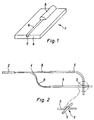
- Figure 1 is a circuit board 1 with an inventive optical waveguide structure shown schematically.
- the Waveguide structure is formed on the circuit board 1.
- she includes lines 2, crossings 3 and branches 4 (if the light the optical fiber from left to right flows through). If the light is in the opposite Direction flowing through the waveguide is with the Numeral 4 denotes a connection.
- Optical fiber structure designed as glass fiber. As well it would be conceivable to use the optical fiber structure in this Training area as plastic fiber.
- the Optical fiber structure In the field of Branches / connections 4 is the Optical fiber structure, however, as a planar Waveguide 6 formed.
- the glass and plastic fibers 5 have the advantage that they have a low optical Have damping, it is not in the area of intersections 3 a scattering or crosstalk of light from one first waveguide crossing into a second Waveguide comes and it does not in the area of intersections 3 there is additional damping.
- the planar Waveguides 6 in turn have the advantage that they have a extremely flexible design of the waveguide structure, in particular branches and / or connections 4, enable.
- the result Glass fibers 5 and the planar waveguide 6 an optimal Optical fiber structure with low attenuation, no scatter in the area of intersections 3 and 1 particularly high flexibility with regard to the course of the Optical waveguide structure, in particular the Lightwave structure branches and connections 4 include.
- trenches 7 in Carrier material 8 introduced.
- the trenches 7 with the help of a photolithographic Introduce the method into the carrier material 8.
- the trenches 7 correspond to the course of the future Waveguide structure.
- the carrier material 8 is as one organic film formed. Be in the trenches 7 initially in the area of lines 2 and intersections 3 the glass fibers 5 introduced and glued. Subsequently the still open areas of the trenches 7, i.e. in the Area of branches and / or connections 4, with filled with a waveguide material that has a higher Refractive index as the material delimiting the trenches 7 having.
- the material defining the trenches 7 corresponds to that Carrier material 8.
- the walls the trenches 7 with an additional special material be coated or lined.
- the Waveguide material is as an optical polymer formed in a flowable state in the Trenches 7 introduced and by means of ultraviolet (UV) radiation is cured.
- planar waveguide 6 from thin glass which has a thickness of a few micrometers (eg 60 ⁇ m ) and whose side walls are structured by an etching process in such a way that light rays inside the waveguide 6 are totally reflected on the side walls become.
- the dimensions of the trenches 7 are chosen so that in Area of lines 2 and intersections 3 the glass fibers 5 can be included at least partially. In the area the trenches 7 are branches and / or connections the dimensions of the planar waveguide 6 accordingly dimensioned.
- the finished circuit board 1 can be part of an optoelectric PCB.
- the optoelectric circuit board is made by at least one of the Metallization levels of a multilayer electrical PCB through an optical layer with the replaced optical waveguide structure according to the invention becomes.
- the electrical layers of the optoelectric Printed circuit board are over optoelectric or electro-optical Transducer coupled to the waveguide structure.
- the optoelectric circuit board is bpsw. a board (e.g. Motherboard) or an assembly of a computer.
- the circuit board 1 according to the invention is particularly suitable for Use in so-called backplane applications where relative large distances must be bridged.
Landscapes
- Physics & Mathematics (AREA)
- General Physics & Mathematics (AREA)
- Optics & Photonics (AREA)
- Optical Integrated Circuits (AREA)
- Optical Couplings Of Light Guides (AREA)
Abstract
Description
- Das Trägermaterial, in dem die Nuten für die Wellenleiter ausgebildet sind, hat die geforderten Eigenschaften (Lichtdurchlässigkeit bei der Wellenlänge des übertragenen Lichts; richtiger Brechungsindex, typischerweise etwa 1% niedriger als der Brechungsindex des Wellenleiterkerns) und die Nuten werden mit einer unteren Cladding-Schicht, der Wellenleiterkernschicht und einer oberen Cladding-Schicht gefüllt.
- Falls das Trägermaterial nicht lichtdurchlässig ist, müssen zunächst der Boden und die Wände der Gräben mit einer Cladding-Schicht überzogen werden, dann wird die Wellenleiterkernschicht in die Gräben gefüllt und schließlich eine obere Cladding-Schicht aufgetragen. Falls die Wellenleiterstruktur keine Verzweigungen umfasst, wäre es auch denkbar, eine Art thermoplastische optische Wellenleiterfaser umfassend den Wellenleiterkern und eine äußere Cladding-Schicht in die Gräben zu pressen.
- Figur 1
- eine schematische Darstellung einer Platine mit einer erfindungsgemäßen Wellenleiterstruktur gemäß einer bevorzugten Ausführungsform in Draufsicht; und
- Figur 2
- die Platine aus Figur 1 im Schnitt.
Claims (11)
- Optische Wellenleiterstruktur, die Leitungen (2), Kreuzungen (3), Verzweigungen (4) und/oder Verbindungen (4) umfasst, umfassend sowohl planare Wellenleiter (6), die aus einem Wellenleitermaterial bestehen, das in Gräben (7) eingebracht ist, die in einem Trägermaterial (8) ausgebildet sind, wobei das Wellenleitermaterial einen höheren Brechungsindex als das die Gräben (7) begrenzende Material hat, als auch Glas- und/oder Kunststofffasern (5), dadurch gekennzeichnet, dass die Wellenleiterstruktur im Bereich der Verzweigungen (4) und der Verbindungen (4) als planare Wellenleiter (6) und im Bereich der Kreuzungen (3) als Glas- und/oder Kunststofffasern (5) ausgebildet ist, die sich im Bereich der Kreuzungen (3) überkreuzen.
- Wellenleiterstruktur nach Anspruch 1, dadurch gekennzeichnet, dass die Wellenleiterstruktur im Bereich der Leitungen (2) als Glas- und/oder Kunststofffasern (5) ausgebildet ist.
- Wellenleiterstruktur nach Anspruch 1 oder 2, dadurch gekennzeichnet, dass das Wellenleitermaterial als ein optisches Polymer ausgebildet ist.
- Wellenleiterstruktur nach einem der Ansprüche 1 bis 3, dadurch gekennzeichnet, dass das Trägermaterial (8) als ein organisches Folienmaterial ausgebildet ist.
- Mehrlagige optoelektrische Leiterplatte, dadurch gekennzeichnet, dass in mindestens einer der Lagen eine Schicht mit einer optischen Wellenleiterstruktur nach einem der Ansprüche 1 bis 4 eingebracht ist.
- Leiterplatte nach Anspruch 5, dadurch gekennzeichnet, dass die elektrischen Schichten der Leiterplatte über optoelektrische Wandler bzw. elektrooptische Wandler mit der optischen Wellenleiterstruktur gekoppelt sind.
- Verfahren zur Herstellung einer optischen Wellenleiterstruktur, die Leitungen (2), Kreuzungen (3), Verzweigungen (4) und/oder Verbindungen (4) umfasst, bei dem in ein Trägermaterial (8) dem Verlauf der Wellenleiterstruktur entsprechende Gräben (7) eingebracht werden, in einem Teil der Gräben (7) Glas- und/oder Kunststofffasern (5) angeordnet werden und in den restlichen Gräben (7) dann ein Wellenleitermaterial (6) eingebracht wird, wobei das Wellenleitermaterial (6) einen höheren Brechungsindex als das die Gräben (7) begrenzende Material aufweist, dadurch gekennzeichnet, dass die Glas- und/oder Kunststofffasern (5) im Bereich der Kreuzungen (3) derart in den Gräben (7) angeordnet werden, dass sie sich im Bereich der Kreuzungen (3) überkreuzen, und dass das Wellenleitermaterial im Bereich der Verzweigungen (4) und Verbindungen (4) in die Gräben (7) eingebracht wird.
- Verfahren nach Anspruch 7, dadurch gekennzeichnet, dass die Glas- und/oder Kunststofffasern (5) im Bereich der Leitungen (2) in den Gräben (7) angeordnet werden, bevor das Wellenleitermaterial (6) in die Gräben (7) eingebracht wird.
- Verfahren nach Anspruch 7 oder 8, dadurch gekennzeichnet, dass das Trägermaterial (8) als ein organisches Folienmaterial ausgebildet ist, in das die Gräben (7) heißgeprägt werden.
- Verfahren nach einem der Ansprüche 7 bis 9, dadurch gekennzeichnet, dass das Wellenleitermaterial (6) als ein optisches Polymer ausgebildet ist, das in einem fließfähigen Zustand in die Gräben (7) eingebracht und mittels Ultraviolett (UV)-Strahlung ausgehärtet wird.
- Verfahren nach einem der Ansprüche 7 bis 10, dadurch gekennzeichnet, dass die Glas- und/oder Kunststofffasern (5) in den Gräben (7) verklebt werden.
Applications Claiming Priority (2)
| Application Number | Priority Date | Filing Date | Title |
|---|---|---|---|
| DE10018283A DE10018283A1 (de) | 2000-04-13 | 2000-04-13 | Optische Wellenleiterstruktur und Verfahren zur Herstellung einer solchen Wellenleiterstruktur |
| DE10018283 | 2000-04-13 |
Publications (3)
| Publication Number | Publication Date |
|---|---|
| EP1152267A2 true EP1152267A2 (de) | 2001-11-07 |
| EP1152267A3 EP1152267A3 (de) | 2004-06-16 |
| EP1152267B1 EP1152267B1 (de) | 2011-06-29 |
Family
ID=7638574
Family Applications (1)
| Application Number | Title | Priority Date | Filing Date |
|---|---|---|---|
| EP01107818A Expired - Lifetime EP1152267B1 (de) | 2000-04-13 | 2001-04-06 | Optische Wellenleiterstruktur und zugehöriges Herstellungsverfahren |
Country Status (4)
| Country | Link |
|---|---|
| US (1) | US6928204B2 (de) |
| EP (1) | EP1152267B1 (de) |
| AT (1) | ATE514966T1 (de) |
| DE (1) | DE10018283A1 (de) |
Families Citing this family (1)
| Publication number | Priority date | Publication date | Assignee | Title |
|---|---|---|---|---|
| US20040005131A1 (en) * | 2002-05-17 | 2004-01-08 | Rantala Juha T. | Materials having low optical loss for waveguides and other optical devices |
Family Cites Families (14)
| Publication number | Priority date | Publication date | Assignee | Title |
|---|---|---|---|---|
| JP3250496B2 (ja) * | 1997-09-19 | 2002-01-28 | 日本電気株式会社 | 光素子実装基板 |
| US3860405A (en) * | 1972-11-13 | 1975-01-14 | Western Electric Co | Bonding of optical components |
| FR2479993A1 (fr) * | 1980-04-04 | 1981-10-09 | Thomson Csf | Commutateur optique a commande mecanique et dispositif optoelectronique autoreparable mettant en oeuvre un tel commutateur |
| US4472020A (en) * | 1981-01-27 | 1984-09-18 | California Institute Of Technology | Structure for monolithic optical circuits |
| EP0146196A3 (de) * | 1983-12-17 | 1987-01-21 | Philips Patentverwaltung GmbH | Integriert-optisches Bauelement |
| DE3741284C2 (de) * | 1987-12-05 | 2000-07-06 | Sel Alcatel Ag | Faseroptischer Mehrfachkoppler |
| US4878727A (en) * | 1988-06-30 | 1989-11-07 | Battelle Memorial Institute | Multimode channel waveguide optical coupling devices and methods |
| JP3066868B2 (ja) * | 1989-11-15 | 2000-07-17 | 三菱瓦斯化学株式会社 | 光分岐器 |
| DE4212208A1 (de) * | 1992-04-10 | 1993-10-14 | Bosch Gmbh Robert | Verfahren zur Herstellung optischer Polymerbauelemente mit integrierter Faser-Chip-Kopplung in Abformtechnik |
| DE4217553C2 (de) * | 1992-05-27 | 2000-06-15 | Quante Ag | Verfahren und Vorrichtung zum Ankoppeln von mit einem Coating versehenen lichtleitenden Fasern für optische Signale der Nachrichtentechnik oder Sensorik an eine integriert-optische Komponente |
| WO1996000996A1 (en) * | 1994-06-30 | 1996-01-11 | The Whitaker Corporation | Planar hybrid optical amplifier |
| US5521992A (en) * | 1994-08-01 | 1996-05-28 | Motorola, Inc. | Molded optical interconnect |
| JP3303555B2 (ja) * | 1994-09-28 | 2002-07-22 | 古河電気工業株式会社 | 複合光導波路カプラ |
| US5943455A (en) * | 1997-04-18 | 1999-08-24 | Lucent Technologies Inc. | Method and apparatus for interfacing optical fibers from optical fiber ribbons and cables with an optical integrated circuit |
-
2000
- 2000-04-13 DE DE10018283A patent/DE10018283A1/de not_active Withdrawn
-
2001
- 2001-04-06 AT AT01107818T patent/ATE514966T1/de active
- 2001-04-06 EP EP01107818A patent/EP1152267B1/de not_active Expired - Lifetime
- 2001-04-12 US US09/832,827 patent/US6928204B2/en not_active Expired - Lifetime
Also Published As
| Publication number | Publication date |
|---|---|
| US20010055457A1 (en) | 2001-12-27 |
| EP1152267B1 (de) | 2011-06-29 |
| EP1152267A3 (de) | 2004-06-16 |
| DE10018283A1 (de) | 2001-10-25 |
| ATE514966T1 (de) | 2011-07-15 |
| US6928204B2 (en) | 2005-08-09 |
Similar Documents
| Publication | Publication Date | Title |
|---|---|---|
| DE112008003784B4 (de) | Flexible, optische Zwischenverbindung | |
| DE69117647T2 (de) | Passiver optischer Wellenleiter | |
| DE602004008003T2 (de) | Optischer Wellenleiter mit Spiegelfläche geformt durch Laserstrahlbearbeitung | |
| AT413891B (de) | Leiterplattenelement mit wenigstens einem licht-wellenleiter sowie verfahren zur herstellung eines solchen leiterplattenelements | |
| DE19838519A1 (de) | Leiterplatte und Verfahren zur Herstellung | |
| DE69926844T2 (de) | Planare Lichtwellenschaltung | |
| DE2827005A1 (de) | Optischer kreis aus polymere | |
| DE112008002057T5 (de) | Photonisches Führungsbauelement | |
| DE3220352A1 (de) | Ebene optische schaltung mit einem lichtkoppler und verfahren zu ihrer herstellung | |
| DE69935129T2 (de) | Ein verfahren zur herstellung von spiegeln in polymerwellenleitern | |
| DE19711121B4 (de) | Verzweigende Lichtwellenleiteranordnung und verzweigendes Lichtwellenleiterarray | |
| EP2219059B1 (de) | Verfahren zur Herstellung einer elektro-optischen Leiterplatte mit Lichtwellenleiterstrukturen | |
| DE112018003324T5 (de) | Bilden von leitfähigen durchkontakten unter verwendung eines lichtleiters | |
| WO2000050946A1 (de) | Leiterplatte für electrische und optische signale sowie verfahren zu deren herstellung | |
| EP2508925A1 (de) | Optisches Kopplungssystem für zwei Lichtwellenleiter | |
| DE20021834U1 (de) | Vorrichtung zur Lichteinkopplung in eine lichtleitende Schicht innerhalb einer hybrid aufgebauten elektrisch-optischen Leiterplatte | |
| EP1152267A2 (de) | Optische Wellenleiterstruktur und zugehöriges Herstellungsverfahren | |
| DE10103273A1 (de) | Optische Wellenleiterstruktur und Verfahren zur Herstellung einer solchen Wellenleiterstruktur | |
| AT12314U1 (de) | Leiterplattenelement und verfahren zur herstellung eines solchen leiterplattenelements | |
| DE2938526C2 (de) | ||
| DE10132794A1 (de) | Kopplung an in Leiterplatten eingebettete Lichtleiter | |
| DE112017001232T5 (de) | Optische Verzweigungs-/Kopplungsvorrichtung und optisches Übertragungs-/Empfangsmodul | |
| WO2018158257A1 (de) | Optoelektronisches bauelement mit laserdiode | |
| DE19930418A1 (de) | Lichtwellenleiter-Bussystem, insbesondere für Backplaneanwendungen, mit durch Sternkoppler verbundenen m-Teilnehmern mit jeweils n-Kanälen | |
| DE10200853B4 (de) | Optische Lage mit optischen Leitern, Leiterplatte, Herstellungsverfahren für optische Lage mit optischen Leitern und Herstellungsverfahren für Leiterplatte |
Legal Events
| Date | Code | Title | Description |
|---|---|---|---|
| PUAI | Public reference made under article 153(3) epc to a published international application that has entered the european phase |
Free format text: ORIGINAL CODE: 0009012 |
|
| AK | Designated contracting states |
Kind code of ref document: A2 Designated state(s): AT BE CH CY DE DK ES FI FR GB GR IE IT LI LU MC NL PT SE TR |
|
| AX | Request for extension of the european patent |
Free format text: AL;LT;LV;MK;RO;SI |
|
| PUAL | Search report despatched |
Free format text: ORIGINAL CODE: 0009013 |
|
| AK | Designated contracting states |
Kind code of ref document: A3 Designated state(s): AT BE CH CY DE DK ES FI FR GB GR IE IT LI LU MC NL PT SE TR |
|
| AX | Request for extension of the european patent |
Extension state: AL LT LV MK RO SI |
|
| 17P | Request for examination filed |
Effective date: 20041020 |
|
| AKX | Designation fees paid |
Designated state(s): AT BE CH CY DE DK ES FI FR GB GR IE IT LI LU MC NL PT SE TR |
|
| RAP1 | Party data changed (applicant data changed or rights of an application transferred) |
Owner name: ALCATEL LUCENT Owner name: ALCATEL SEL AKTIENGESELLSCHAFT |
|
| GRAP | Despatch of communication of intention to grant a patent |
Free format text: ORIGINAL CODE: EPIDOSNIGR1 |
|
| RIC1 | Information provided on ipc code assigned before grant |
Ipc: G02B 6/125 20060101AFI20110113BHEP |
|
| GRAS | Grant fee paid |
Free format text: ORIGINAL CODE: EPIDOSNIGR3 |
|
| GRAA | (expected) grant |
Free format text: ORIGINAL CODE: 0009210 |
|
| AK | Designated contracting states |
Kind code of ref document: B1 Designated state(s): AT BE CH CY DE DK ES FI FR GB GR IE IT LI LU MC NL PT SE TR |
|
| REG | Reference to a national code |
Ref country code: GB Ref legal event code: FG4D Free format text: NOT ENGLISH |
|
| REG | Reference to a national code |
Ref country code: CH Ref legal event code: EP |
|
| REG | Reference to a national code |
Ref country code: IE Ref legal event code: FG4D Free format text: LANGUAGE OF EP DOCUMENT: GERMAN |
|
| REG | Reference to a national code |
Ref country code: DE Ref legal event code: R096 Ref document number: 50115914 Country of ref document: DE Effective date: 20110818 |
|
| REG | Reference to a national code |
Ref country code: NL Ref legal event code: VDEP Effective date: 20110629 |
|
| PG25 | Lapsed in a contracting state [announced via postgrant information from national office to epo] |
Ref country code: SE Free format text: LAPSE BECAUSE OF FAILURE TO SUBMIT A TRANSLATION OF THE DESCRIPTION OR TO PAY THE FEE WITHIN THE PRESCRIBED TIME-LIMIT Effective date: 20110629 |
|
| PG25 | Lapsed in a contracting state [announced via postgrant information from national office to epo] |
Ref country code: FI Free format text: LAPSE BECAUSE OF FAILURE TO SUBMIT A TRANSLATION OF THE DESCRIPTION OR TO PAY THE FEE WITHIN THE PRESCRIBED TIME-LIMIT Effective date: 20110629 Ref country code: GR Free format text: LAPSE BECAUSE OF FAILURE TO SUBMIT A TRANSLATION OF THE DESCRIPTION OR TO PAY THE FEE WITHIN THE PRESCRIBED TIME-LIMIT Effective date: 20110930 |
|
| REG | Reference to a national code |
Ref country code: IE Ref legal event code: FD4D |
|
| PG25 | Lapsed in a contracting state [announced via postgrant information from national office to epo] |
Ref country code: PT Free format text: LAPSE BECAUSE OF FAILURE TO SUBMIT A TRANSLATION OF THE DESCRIPTION OR TO PAY THE FEE WITHIN THE PRESCRIBED TIME-LIMIT Effective date: 20111031 Ref country code: NL Free format text: LAPSE BECAUSE OF FAILURE TO SUBMIT A TRANSLATION OF THE DESCRIPTION OR TO PAY THE FEE WITHIN THE PRESCRIBED TIME-LIMIT Effective date: 20110629 Ref country code: IE Free format text: LAPSE BECAUSE OF FAILURE TO SUBMIT A TRANSLATION OF THE DESCRIPTION OR TO PAY THE FEE WITHIN THE PRESCRIBED TIME-LIMIT Effective date: 20110629 |
|
| RAP2 | Party data changed (patent owner data changed or rights of a patent transferred) |
Owner name: ALCATEL LUCENT Owner name: ALCATEL SEL AKTIENGESELLSCHAFT |
|
| PG25 | Lapsed in a contracting state [announced via postgrant information from national office to epo] |
Ref country code: CY Free format text: LAPSE BECAUSE OF FAILURE TO SUBMIT A TRANSLATION OF THE DESCRIPTION OR TO PAY THE FEE WITHIN THE PRESCRIBED TIME-LIMIT Effective date: 20110629 |
|
| REG | Reference to a national code |
Ref country code: CH Ref legal event code: PCOW Free format text: ALCATEL LUCENT;3, AVENUE OCTAVE GREARD;75007 PARIS (FR) |
|
| PLBE | No opposition filed within time limit |
Free format text: ORIGINAL CODE: 0009261 |
|
| STAA | Information on the status of an ep patent application or granted ep patent |
Free format text: STATUS: NO OPPOSITION FILED WITHIN TIME LIMIT |
|
| PG25 | Lapsed in a contracting state [announced via postgrant information from national office to epo] |
Ref country code: IT Free format text: LAPSE BECAUSE OF FAILURE TO SUBMIT A TRANSLATION OF THE DESCRIPTION OR TO PAY THE FEE WITHIN THE PRESCRIBED TIME-LIMIT Effective date: 20110629 |
|
| 26N | No opposition filed |
Effective date: 20120330 |
|
| PG25 | Lapsed in a contracting state [announced via postgrant information from national office to epo] |
Ref country code: DK Free format text: LAPSE BECAUSE OF FAILURE TO SUBMIT A TRANSLATION OF THE DESCRIPTION OR TO PAY THE FEE WITHIN THE PRESCRIBED TIME-LIMIT Effective date: 20110629 |
|
| REG | Reference to a national code |
Ref country code: DE Ref legal event code: R097 Ref document number: 50115914 Country of ref document: DE Effective date: 20120330 |
|
| BERE | Be: lapsed |
Owner name: ALCATEL SEL A.G. Effective date: 20120430 Owner name: ALCATEL LUCENT Effective date: 20120430 |
|
| PG25 | Lapsed in a contracting state [announced via postgrant information from national office to epo] |
Ref country code: MC Free format text: LAPSE BECAUSE OF NON-PAYMENT OF DUE FEES Effective date: 20120430 |
|
| REG | Reference to a national code |
Ref country code: CH Ref legal event code: PL |
|
| PG25 | Lapsed in a contracting state [announced via postgrant information from national office to epo] |
Ref country code: CH Free format text: LAPSE BECAUSE OF NON-PAYMENT OF DUE FEES Effective date: 20120430 Ref country code: LI Free format text: LAPSE BECAUSE OF NON-PAYMENT OF DUE FEES Effective date: 20120430 Ref country code: BE Free format text: LAPSE BECAUSE OF NON-PAYMENT OF DUE FEES Effective date: 20120430 |
|
| PG25 | Lapsed in a contracting state [announced via postgrant information from national office to epo] |
Ref country code: ES Free format text: LAPSE BECAUSE OF FAILURE TO SUBMIT A TRANSLATION OF THE DESCRIPTION OR TO PAY THE FEE WITHIN THE PRESCRIBED TIME-LIMIT Effective date: 20111010 |
|
| REG | Reference to a national code |
Ref country code: AT Ref legal event code: MM01 Ref document number: 514966 Country of ref document: AT Kind code of ref document: T Effective date: 20120406 |
|
| REG | Reference to a national code |
Ref country code: FR Ref legal event code: CD Owner name: ALCATEL LUCENT, FR Effective date: 20130531 Ref country code: FR Ref legal event code: CD Owner name: ALCATEL-LUCENT DEUTSCHLAND AG Effective date: 20130531 |
|
| PG25 | Lapsed in a contracting state [announced via postgrant information from national office to epo] |
Ref country code: AT Free format text: LAPSE BECAUSE OF NON-PAYMENT OF DUE FEES Effective date: 20120406 |
|
| REG | Reference to a national code |
Ref country code: FR Ref legal event code: GC Effective date: 20131018 |
|
| PG25 | Lapsed in a contracting state [announced via postgrant information from national office to epo] |
Ref country code: TR Free format text: LAPSE BECAUSE OF FAILURE TO SUBMIT A TRANSLATION OF THE DESCRIPTION OR TO PAY THE FEE WITHIN THE PRESCRIBED TIME-LIMIT Effective date: 20110629 |
|
| PG25 | Lapsed in a contracting state [announced via postgrant information from national office to epo] |
Ref country code: LU Free format text: LAPSE BECAUSE OF NON-PAYMENT OF DUE FEES Effective date: 20120406 |
|
| REG | Reference to a national code |
Ref country code: FR Ref legal event code: RG Effective date: 20141016 |
|
| REG | Reference to a national code |
Ref country code: FR Ref legal event code: PLFP Year of fee payment: 15 |
|
| REG | Reference to a national code |
Ref country code: FR Ref legal event code: PLFP Year of fee payment: 16 |
|
| REG | Reference to a national code |
Ref country code: FR Ref legal event code: PLFP Year of fee payment: 17 |
|
| PGFP | Annual fee paid to national office [announced via postgrant information from national office to epo] |
Ref country code: GB Payment date: 20170419 Year of fee payment: 17 Ref country code: DE Payment date: 20170419 Year of fee payment: 17 Ref country code: FR Payment date: 20170419 Year of fee payment: 17 |
|
| REG | Reference to a national code |
Ref country code: DE Ref legal event code: R119 Ref document number: 50115914 Country of ref document: DE |
|
| GBPC | Gb: european patent ceased through non-payment of renewal fee |
Effective date: 20180406 |
|
| PG25 | Lapsed in a contracting state [announced via postgrant information from national office to epo] |
Ref country code: DE Free format text: LAPSE BECAUSE OF NON-PAYMENT OF DUE FEES Effective date: 20181101 |
|
| PG25 | Lapsed in a contracting state [announced via postgrant information from national office to epo] |
Ref country code: GB Free format text: LAPSE BECAUSE OF NON-PAYMENT OF DUE FEES Effective date: 20180406 |
|
| REG | Reference to a national code |
Ref country code: DE Ref legal event code: R082 Ref document number: 50115914 Country of ref document: DE Representative=s name: MENZIETTI WETZEL, DE Ref country code: DE Ref legal event code: R081 Ref document number: 50115914 Country of ref document: DE Owner name: PROVENANCE ASSET GROUP LLC, PITTSFORD, US Free format text: FORMER OWNER: ALCATEL SEL AG, 70435 STUTTGART, DE |
|
| PG25 | Lapsed in a contracting state [announced via postgrant information from national office to epo] |
Ref country code: FR Free format text: LAPSE BECAUSE OF NON-PAYMENT OF DUE FEES Effective date: 20180430 |