EP1151446B1 - Mikroschaltkontakt - Google Patents
Mikroschaltkontakt Download PDFInfo
- Publication number
- EP1151446B1 EP1151446B1 EP00902631A EP00902631A EP1151446B1 EP 1151446 B1 EP1151446 B1 EP 1151446B1 EP 00902631 A EP00902631 A EP 00902631A EP 00902631 A EP00902631 A EP 00902631A EP 1151446 B1 EP1151446 B1 EP 1151446B1
- Authority
- EP
- European Patent Office
- Prior art keywords
- contact
- microswitching
- base plate
- bending beam
- contact according
- Prior art date
- Legal status (The legal status is an assumption and is not a legal conclusion. Google has not performed a legal analysis and makes no representation as to the accuracy of the status listed.)
- Expired - Lifetime
Links
Images



Classifications
-
- H—ELECTRICITY
- H01—ELECTRIC ELEMENTS
- H01H—ELECTRIC SWITCHES; RELAYS; SELECTORS; EMERGENCY PROTECTIVE DEVICES
- H01H1/00—Contacts
- H01H1/0036—Switches making use of microelectromechanical systems [MEMS]
-
- H—ELECTRICITY
- H01—ELECTRIC ELEMENTS
- H01H—ELECTRIC SWITCHES; RELAYS; SELECTORS; EMERGENCY PROTECTIVE DEVICES
- H01H1/00—Contacts
- H01H1/02—Contacts characterised by the material thereof
- H01H1/021—Composite material
-
- H—ELECTRICITY
- H01—ELECTRIC ELEMENTS
- H01H—ELECTRIC SWITCHES; RELAYS; SELECTORS; EMERGENCY PROTECTIVE DEVICES
- H01H1/00—Contacts
- H01H1/0036—Switches making use of microelectromechanical systems [MEMS]
- H01H2001/0052—Special contact materials used for MEMS
- H01H2001/0057—Special contact materials used for MEMS the contact materials containing refractory materials, e.g. tungsten
-
- H—ELECTRICITY
- H01—ELECTRIC ELEMENTS
- H01H—ELECTRIC SWITCHES; RELAYS; SELECTORS; EMERGENCY PROTECTIVE DEVICES
- H01H50/00—Details of electromagnetic relays
- H01H50/005—Details of electromagnetic relays using micromechanics
-
- H—ELECTRICITY
- H01—ELECTRIC ELEMENTS
- H01H—ELECTRIC SWITCHES; RELAYS; SELECTORS; EMERGENCY PROTECTIVE DEVICES
- H01H59/00—Electrostatic relays; Electro-adhesion relays
- H01H59/0009—Electrostatic relays; Electro-adhesion relays making use of micromechanics
Definitions
- the present invention relates to a mechanical closing electrical micro switch contact.
- Such switch contacts are everywhere there needed where large electrical currents are confined Room should be switched, for example in Sensors, actuators and high-performance / high-temperature applications, such as in power electronics, Automotive electronics or in chemically aggressive Environments.
- a micro switch contact according to the generic term of claim 1 is e.g. known from US-A-4954170.
- Micromechanical switches are compared to conventional ones Relays fast, shock resistant and need very little control power with electrostatic Drive and also usually have negligible Control leakage currents. Miniaturization also allows implementation in microwave circuits, where high power pulse operation is required is.
- Micro switches and micro relays can be used on the electrostatic (capacitive), magnetic or inductive principle or based on temperature change be switchable.
- Microswitches are generally based on silicon or metal or ceramic micromechanical concepts. This is usually coated with silicon dioxide Silicon as an electrically insulating substrate, while the contacts from different Multi-layer material systems exist. For the production is therefore a complex material system and a correspondingly complex procedure is required.
- the currents to be switched are metallic or silicon-based microswitches, there at high current densities due to the heat loss of the switch often very high temperatures arise that no longer with these materials are manageable.
- hybrid structures exist or ceramic switches. With these, however the respective material thickness, for example one Bending beam, limited at the bottom.
- the object of the present invention is therefore a mechanically closing, electrical micro switch contact to provide the chemically is inert, long life, high impact resistance, high switching dynamics, minimal material complexity has, which is suitable for microwave, at very high temperatures and a can switch high current density.
- the micro switch contact according to the invention has two electrically conductive contact elements which, in the closed state, touch in the region of two electrically conductive contact surfaces. At least one of the two contact surfaces consists of highly doped, conductive and therefore quasi-metallic diamond, silicon carbide (SiC), galium nitride (GaN), boron nitride (BN), aluminum nitride (AlN) and / or aluminum gallium nitride (AlGaN). Diamond in particular is characterized by a high debye temperature and is therefore elastic up to high temperatures and has a high temperature conductivity. Furthermore, these materials have the property that their electrical properties can be changed by doping between insulating, semiconducting and quasi-metallic.
- Diamond also has high wear resistance and mechanical stability, which leads to a long service life of the switch contact.
- the microswitch according to the invention can be used at very high temperatures, for example up to 800 ° C., and switch a high current density (with high power loss), for example of 1 ⁇ 10 6 A / cm 2 at an operating temperature of ⁇ 600 ° C. These properties are made possible by a single base material. Because there is no plastic deformation, even at high temperatures in diamond, there is no change in the threshold voltage at temperatures themselves T> 600 ° C to be expected.
- micro switch contact according to the invention possible very small freestanding To produce layer structures, for example bending beams with a thickness between usually 0.5 to 10 ⁇ m. This reduces the inertia of the moving elements and thus increases the switching dynamics.
- layer thicknesses with high bending stiffness and Breaking strength are with ceramic and hybrid construction currently not feasible.
- one or preferably both Contact surfaces of the contact elements made of diamond, SiC, AlN, BN, GaN and / or AlGaN exist.
- at least one of the two contact surfaces partly made of metal (Al, Au, Cu, Ni), a carbide-forming Metal and / or a high temperature stable Metallization exist.
- the high temperature stable Metallization can contain W: Si and / or Ta: Si.
- One of the two contact surfaces is advantageously each on a base plate and / or a bending beam arranged.
- the bending beam is preferred cantilevered over one arranged at one of its ends Anchor or other mechanical connection fixed.
- Both the base plate and the anchor or the bending beam can be from one of the above mentioned materials diamond, SiC, GaN, AlN, BN and / or AlGaN exist.
- BN for all layers and elements of the invention
- Micro switch contact cubic boron nitride used as BN for all layers and elements of the invention.
- the bending beam Due to the electrostatic, inductive, hydraulic, pneumatic, mechanical and / or thermomechanical principle in the direction the bottom plate are moved so that the touch opposite contact elements and create an electrical contact.
- the Currents to the two contact elements can be via respective External contacts, for example on the first Contact element or on the bending beam as metallization are applied, are supplied.
- control electrode can be attached via by means of the electrostatic principle of the bending beams be moved in the direction of the base plate can. Also on this control electrode are on the side outside the area covered by the bending beam Metallizations as external contacts to put on arranged the control voltage.
- the contacting of the contact elements and the control electrode can also use the so-called via-hole technique take place at the corresponding holes in the Bottom plate are etched on the back, so that on the back the corresponding components to be contacted exposed and with a metallization as external contact can be covered.
- the entire component constructed from a single material such as diamond.
- a single material such as diamond.
- doping achieved that, for example the contact elements, the control electrode and the Bending beams are electrically conductive, for example by strong doping, for example with boron, nitrogen, Sulfur or phosphorus.
- the entire component can be arranged on a carrier layer, for example made of silicon. This can also be present during the production of the component and can be removed later.
- a further insulating layer for example made of SiO x , can be arranged between the base plate and the carrier layer in order to prevent any leakage currents through the carrier material.
- the manufacture of an anchored Switching contact take place by first the bottom plate, the anchor and the first contact element as well optionally the control electrode on a silicon carrier, for example via CVD methods, preferably Plasma CVD but also via arc jet CVD or hot filament CVD be deposited. Then a Victim layer applied to which the Bending beam is deposited. The bending beam is connected to the anchor and thus the base plate, so that the victim layer is then removed and the bending beam as a self-supporting mechanical Component remains.
- CVD methods preferably Plasma CVD but also via arc jet CVD or hot filament CVD be deposited.
- FIG. 1 shows a micro switch contact according to the invention 1.
- the micro switch contact 1 is located a base plate on a carrier layer 2 made of silicon 3 from undoped and thus non-conductive, Diamond deposited using a CVD process.
- a carrier layer 2 made of silicon 3 from undoped and thus non-conductive, Diamond deposited using a CVD process.
- On one The end of the bottom plate is another non-conductive Diamond layer applied as anchor 4.
- At the other The end of the base plate 3 is a contact element 7 made of heavily doped with boron and therefore quasi-metallic conductive diamond arranged.
- a bending beam 5 also from a strong boron doping quasi-metallic conductive Diamond.
- the height of the armature 4 determines the distance of the bending beam 5 from the base plate 3.
- This Bending beam 5 extends cantilever to the first contact element 7, where on its underside a second contact element 8 made of electrically conductive Diamond is arranged.
- the two contact elements 7 and 8 have a predetermined in the non-switched state Distance from each other.
- control electrode 9 made of electrically conductive diamond.
- Both the control electrode 9 and the first one Contact element 7 have metallizations made of W: Si or Au 11 or 10, which act as external contacts of voltages and currents to the control electrode 9 and the first contact element 7 are used.
- This Metallizations 11 and 10 are out of range attached, which is covered by the bending beam 5 becomes. This will make contact between the Bending beam 5 and the metallizations 11 and 10 avoided, if the bending beam is in the direction of the Arrow A bends.
- the second contact element 8 is over the bending beam 5 with one attached to this bending beam, as Metallization 6 serving external contact electrically connected. Voltage can be applied to this metallization 6 the second contact element 8 are created.
- About the thickness and the dimensioning of the bending beam 5 can change its elastic properties be so that, for example, the threshold voltage or the switching limit frequency individually can be adjusted.
- the base plate 3 of the micro switch contact instead of diamond SiC, GaN, AlN, AlGaN or BN exist.
- the carrier 2 advantageously consists of (100) -oriented silicon.
- the base plate 3 can be high be oriented and have a high surface planarity have.
- the second contact 8 can also from a high temperature stable metallization like W: Si or Ta: Si exist.
- the second contact element 8 made of diamond and the first Contact element 7 from such a high temperature stable Metallization exist.
- the metallization can even be done on a diamond substrate ("metal coated Diamond "), the good mechanical ones Properties of the diamond can be used. such metallizations are stable at high temperatures for example of high temperature stable Schottky diode materials known from here.
- the switch contact 1 shown in FIG. 1 becomes capacitive here (electrostatic) switched.
- As an upper capacitor plate serves the bending beam 5 and as lower electrode the control electrode 9.
- the switching voltage between a few volts and a few 10 volts become.
- the Bending beam 5 has a thickness between 0.5 and 10 ⁇ m. This low layer thicknesses lead just like the high one Modulus of elasticity of diamond to a low inertia and thus high switching limit frequency.
- Such small layer thicknesses for bending beams are with one Ceramic or hybrid construction not possible.
- Figure 2 shows the measured temperature dependence the threshold voltage of the micro switch contact shown in FIG. 1 1. It is easy to see that switching up to temperatures well above 600 ° C possible without changing the threshold voltage is.
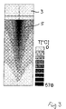
- FIG. 3 shows the simulated temperature distribution in the vacuum of the micro switch contact 1 shown in FIG. 1 at a current density of 1 ⁇ 10 6 A / cm 2 .
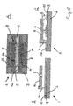
- FIG 4 shows another example of an inventive Micro switch contact, with the shields are intended for HF frequencies.
- the shields are intended for HF frequencies.
- FIG. 4 shows another example of an inventive Micro switch contact, with the shields are intended for HF frequencies.
- FIG. 4 shows another example of an inventive Micro switch contact, with the shields are intended for HF frequencies.
- FIG. 4 shows another example of an inventive Micro switch contact, with the shields are intended for HF frequencies.
- the armature is now 4 a bending beam 5 attached, the three different, metallizations 6a electrically separated from one another, 6b and 6c.
- the bending beam itself is out electrically insulating diamond during the metallization 6a, 6b, 6c each with contact elements 8a, 8b and 8c are connected.
- FIG. 4A The metallizations 6a, 6b and 6c are on the side of the armature 4 with further metallizations 12a, 12b and 12c connected.
- the bending beam thus supports 5 a total of 3 shift fingers, the middle one Switch finger with the metallization 6b to the signal line is used while the other two Shift finger with the metallizations 6a and 6c Shield are connected to ground.
- the bending beam 5 is now bent by the Control electrode 9 applied a corresponding voltage the contact elements 6a, 6b and 6c with the corresponding contact elements 7a, 7b and 7c connected to the diamond substrate 3.
- the metallizations 12a, 12b and 12c with the metallizations 10a, 10b and 10c produced. That’s not all Signal, but also the appropriate ground shield connected through.
- Figure 4B shows a cross section through each of the individual Shift finger, it should be noted that all Shift finger arranged on the same bending beam 5 are.
- the indices a, b and c have been omitted here, because each of these shift fingers is constructed the same way is.
- FIG. 5 shows a further invention Switching contact, which also has three fingers, however only the middle signal contact is switched becomes.
- FIG. 5 as in FIG. 4, corresponding elements with corresponding reference numerals as provided in Figure 1, so that on their description is waived.
- FIG. 5B shows a cross section through a mass-leading switch contact, in which a metallization 14 is applied to the common bending beam 5. Furthermore, a metallization 13 is arranged between the insulating diamond layer 3 and the armature 4, which extends over the entire length of the switching finger and connects both sides of the switching contact to one another as a ground shield.
- the metallization 14 on the bending beam 5 serves as a control electrode. Both the metallization 13 and the metallization 14 can consist, for example, of W: Si, W: Si: N, Ti, Au, possibly also with a P + diamond layer underneath.
- the bending beam 5 is designed semi-insulating in this example.
- FIG. 5C shows the middle shift finger, which acts as a signal line.
- This Switch contact is designed in the same way as the switching contact, which is shown in Figure 4B, and is therefore not described further here.
- FIG 5A is a top view of the entire Switching contact shown, which can be seen here is that only the middle shift finger at one Deflection of the bending beam 5 an electrical Contact between the two contact elements 7 and 8 manufactures.
- the bar 5 becomes electrostatic by applying a voltage between the beam contact 14 and the substrate ground surface 13 deflected. This will make the diamond contact over the contact elements 7, 8 closed and there can be a signal current via the metallization 12, 6, via the contact elements 8, 7 and the metallization 10 flow.
- the beam metallizations 14 for the control voltage are from the underlying and mass substrate metallization 13 via the insulating anchor 4 electrically isolated.
- the two signal metallizations 6 are with the substrate signal metallization 12th connected, the two metallizations 12 and 13 and the two metallizations 10 and 13 each spatially and thus also electrically from each other are separated.
- Micro switch contact it becomes possible very to switch high currents at very high temperatures. It is particularly exploited that diamond is dependent from its doping, very variable electrical Possesses properties and as multifunctional Material can be used. Diamond has one high thermal conductivity and high heat resistance.
- the microswitch according to the invention is chemical inert, has a long life, high Impact resistance, high switching dynamics and minimal Complexity of materials and is suitable for microwaves.
Landscapes
- Physics & Mathematics (AREA)
- Electromagnetism (AREA)
- Contacts (AREA)
- Micromachines (AREA)
- Mechanical Treatment Of Semiconductor (AREA)
- Push-Button Switches (AREA)
Description
T > 600 °C zu erwarten.
- Figur 1
- einen erfindungsgemäßen Mikroschaltkontakt;
- Figur 2
- die Temperaturabhängigkeit der Schwellspannung des Schaltkontaktes aus Figur 1;
- Figur 3
- die Simulation der Temperaturverteilung im Vakuum des Mikroschaltkontaktes aus Figur 1;
- Figur 4
- einen Schaltkontakt mit einem geschalteten Schaltkontakt und zwei Abschirmungen sowie
- Figur 5
- einen Schaltkontakt mit geschaltetem Signalkontakt und zwei geschalteten Abschirmungen.
Claims (30)
- Mechanisch schließender, elektrischer Mikroschaltkontakt mit einem ersten und einem zweiten elektrisch leitenden Kontaktelement mit einer ersten bzw. einer zweiten elektrisch leitenden Kontaktfläche, wobei die beiden Kontaktelemente im offenen Zustand des Mikroschaltkontakts einen vorbestimmten Abstand voneinander aufweisen und im geschlossenen Zustand einander in einem Kontaktbereich im Bereich der ersten und zweiten Kontaktflächen berühren, dadurch gekennzeichnet, daß das erste Kontaktelement an einem Ende eines Biegebalkens aus Diamant angeordnet ist und die erste Kontaktfläche und/oder die zweite Kontaktfläche zumindest teilweise aus einem karbidbildenden Metall, einer hochtemperaturstabilen Metallisierung, hochdotiertem, leitfähigem Diamant, Siliziumcarbid (SiC), Galiumnitrid (GaN), Bornitrid (BN), Aluminium-Galiumnitrid (AlGaN) und/oder Aluminiuminitirid (AlN) besteht.
- Mikroschaltkontakt nach dem vorhergehenden Anspruch, dadurch gekennzeichnet, daß eine der beiden Kontaktflächen zumindest teilweise aus Metall, einem karbidbildenden Metall und/oder einer hochtemperaturstabilen Metallisierung besteht.
- Mikroschaltkontakt nach dem vorhergehenden Anspruch, dadurch gekennzeichnet, daß die hochtemperaturstabile Metallisierung W:Si und/oder Ta:Si enthält.
- Mikroschaltkontakt nach einem der vorhergehenden Ansprüche, gekennzeichnet durch
eine Bodenplatte, wobei auf der Oberseite der Bodenplatte das erste Kontaktelement derart angeordnet ist, daß seine Kontaktfläche der Bodenplatte gegenüber liegt,
einen Anker, der auf der Oberseite der Bodenplatte in einem vorbestimmten Abstand zu dem ersten Kontaktelement angeordnet ist,
wobei der Biegebalken auf der der Bodenplatte abgewandten Seite des Ankers befestigt ist, von diesem in einem vorbestimmten Abstand zur Bodenplatte gehalten wird und sich freitragend von dem Anker bis zum ersten Kontaktelement erstreckt und
wobei das zweite Kontaktelement auf der dem ersten Kontaktelement zugewandten Seite des Biegebalkens angeordnet ist, derart, daß die Kontaktfläche des zweiten Kontaktelementes der Kontaktfläche des ersten Kontaktelementes gegenüber liegt. - Mikroschaltkontakt nach dem vorhergehenden Anspruch, dadurch gekennzeichnet, daß die Bodenplatte zumindest teilweise aus einer elektrisch isolierenden Diamantschicht, SiC, GaN, AlGaN, BN und/oder AlN besteht.
- Mikroschaltkontakt nach einem der beiden vorhergehenden Ansprüche, dadurch gekennzeichnet, daß der Anker zumindest teilweise aus elektrisch isolierendem Diamant, SiC, GaN, AlGaN, BN und/oder AlN besteht derart, daß er die Bodenplatte und den Biegebalken voneinander elektrisch isoliert.
- Mikroschaltkontakt nach einem der drei vorhergehenden Ansprüche, dadurch gekennzeichnet, daß der Biegebalken zumindest teilweise aus elektrisch leitend dotiertem Diamant, SiC, GaN, AlGaN, BN und/oder AlN besteht.
- Mikroschaltkontakt nach einem der Ansprüche 4 bis 7, dadurch gekennzeichnet, daß der Biegebalken in Richtung senkrecht zur Oberfläche der Bodenplatte eine Dicke zwischen 0,5 und 10 µm aufweist.
- Mikroschaltkontakt nach einem der Ansprüche 4 bis 8, dadurch gekennzeichnet, daß die Bodenplatte auf einem Substrat als Träger angeordnet ist.
- Mikroschaltkontakt nach dem vorhergehenden Anspruch, dadurch gekennzeichnet, daß das Substrat zumindest teilweise aus Silizium besteht.
- Mikroschaltkontakt nach dem vorhergehenden Anspruch, dadurch gekennzeichnet, daß das Substrat zumindest teilweise aus (100)-orientiertem Silizium besteht.
- Mikroschaltkontakt nach einem der Ansprüche 4 bis 11, dadurch gekennzeichnet, daß er elektrostatisch, induktiv, mechanisch und/oder thermodynamisch schaltbar ist.
- Mikroschaltkontakt nach dem vorhergehenden Anspruch, dadurch gekennzeichnet, daß auf der Bodenplatte zwischen der Bodenplatte und dem Biegebalken eine Steuerelektrode angeordnet ist.
- Mikroschaltkontakt nach dem vorhergehenden Anspruch, dadurch gekennzeichnet, daß die Steuerelektrode zumindest teilweise aus elektrisch leitend dotiertem Diamant besteht.
- Mikroschaltkontakt nach einem der beiden vorhergehenden Ansprüche, dadurch gekennzeichnet, daß die Steuerelektrode elektrische Außenkontakte zur Spannungsversorgung der Steuerelektrode aufweist.
- Mikroschaltkontakt nach einem der vorhergehenden Ansprüche, dadurch gekennzeichnet, daß an dem ersten und/oder zweiten Kontaktelement außerhalb des Kontaktbereichs elektrische Außenkontakte zur Spannungs- und Stromversorgung des Kontaktelementes angeordnet sind.
- Mikroschaltkontakt nach dem vorhergehenden Anspruch, dadurch gekennzeichnet, daß das erste und/oder zweite Kontaktelement außerhalb des Kontaktbereichs mit Oberflächenmetallisierungen zur Bildung der elektrischen Außenkontakte versehen sind.
- Mikroschaltkontakt nach Anspruch 15, dadurch gekennzeichnet, daß die Steuerelektrode mit Oberflächenmetallisierungen zur Bildung der elektrischen Außenkontakte versehen ist.
- Mikroschaltkontakt nach einem der Ansprüche 4 bis 18, dadurch gekennzeichnet, daß die Oberfläche des Biegebalkens zumindest teilweise Oberflächenmetallisierungen aufweist.
- Mikroschaltkontakt nach dem vorhergehenden Anspruch, dadurch gekennzeichnet, daß die dem Anker entgegengesetzte Oberfläche des Biegebalkens zumindest teilweise Oberflächenmetallisierungen aufweist.
- Mikroschaltkontakt nach einem der Ansprüche 17 bis 20, dadurch gekennzeichnet, daß die Oberflächenmetallisierung ein Edelmetall, ein Nichtedelmetall oder eine Metalllegierung aufweist.
- Mikroschaltkontakt nach dem vorhergehenden Anspruch, dadurch gekennzeichnet, daß die Oberflächenmetallisierung durch Aufdampfen, Zerstäuben oder galvanische Abscheidung auf die Kontaktelemente, den Biegebalken und/oder die Steuerelektrode aufgebracht ist.
- Mikroschaltkontakt nach einem der Ansprüche 4 bis 22, dadurch gekennzeichnet, daß die Bodenplatte und ggf. der Träger im Bereich des ersten Kontaktelementes und gegebenenfalls im Bereich der Steuerelektrode auf der von diesen abgewancten Seite Öffnungen aufweisen, über die das erste Kontaktelement und gegebenenfalls die Steuerelektrode elektrisch kontaktierbar sind.
- Mikroschaltkontakt nach einem der Ansprüche 4 bis 23, dadurch gekennzeichnet, daß zwischen dem Träger und der Bodenplatte eine Zwischenschicht aus Silizium(di)oxid (SiOx), Siliziumnitrid, Metall, einer Legierung und/oder einem Dielektrikum angeordnet ist.
- Mikroschaltkontakt nach einem der Ansprüche 4 bis 24, dadurch gekennzeichnet, daß die Bodenplatte, der Anker und/oder der Biegebalken durch chemische Gasphasenabscheidung (CVD-Verfahren) von Diamant hergestellt ist.
- Mikroschaltkontakt nach dem vorhergehenden Anspruch, dadurch gekennzeichnet, daß der Diamant durch Plasma-CVD, Arc-Jet-CVD, und/oder Hot-Filament-CVD abgeschieden ist.
- Mikroschaltkontakt nach einem der vorhergehenden Ansprüche, dadurch gekennzeichnet, daß die elektrisch leitfähigen Diamantschichten der Kontaktelemente, des Biegebalkens und/oder der Steuerelektrode zumindest teilweise aus Diamantschichten bestehen, der mit Bor, Stickstoff, Schwefel und/oder Phosphor dotiert sind.
- Verfahren zur Herstellung eines Mikroschaltkontaktes nach einem der Ansprüche 4 bis 27,
dadurch gekennzeichnet, daß
auf einem Träger eine Bodenplatte, ein Anker und das erste Kontaktelement aufgebracht,
auf die Bodenplatte bis zur Höhe des Ankers eine Opferschicht aufgebracht,
auf den Anker und die Opferschicht der Biegebalken und das mit dem Biegebalken verbundene zweite Kontaktelement aufgebracht wird,
und abschließend die Opferschicht entfernt wird. - Verfahren nach dem vorhergehenden Anspruch, dadurch gekennzeichnet, daß eine Opferschicht aus Metall, einem Dielektrikum, Siliziumdioxid, SiOx, Si3N4 und/oder SiOxNy aufgebracht wird.
- Verfahren nach einem der beiden vorhergehenden Ansprüche, dadurch gekennzeichnet, daß die Opferschicht durch Ätzen entfernt wird.
Applications Claiming Priority (3)
| Application Number | Priority Date | Filing Date | Title |
|---|---|---|---|
| DE19902868 | 1999-01-25 | ||
| DE19902868 | 1999-01-25 | ||
| PCT/EP2000/000552 WO2000044012A1 (de) | 1999-01-25 | 2000-01-25 | Mikroschaltkontakt |
Publications (2)
| Publication Number | Publication Date |
|---|---|
| EP1151446A1 EP1151446A1 (de) | 2001-11-07 |
| EP1151446B1 true EP1151446B1 (de) | 2003-05-07 |
Family
ID=7895324
Family Applications (1)
| Application Number | Title | Priority Date | Filing Date |
|---|---|---|---|
| EP00902631A Expired - Lifetime EP1151446B1 (de) | 1999-01-25 | 2000-01-25 | Mikroschaltkontakt |
Country Status (6)
| Country | Link |
|---|---|
| EP (1) | EP1151446B1 (de) |
| JP (1) | JP2003527727A (de) |
| AT (1) | ATE239974T1 (de) |
| AU (1) | AU2440000A (de) |
| DE (2) | DE10080131D2 (de) |
| WO (1) | WO2000044012A1 (de) |
Families Citing this family (39)
| Publication number | Priority date | Publication date | Assignee | Title |
|---|---|---|---|---|
| US6396368B1 (en) * | 1999-11-10 | 2002-05-28 | Hrl Laboratories, Llc | CMOS-compatible MEM switches and method of making |
| US6426722B1 (en) | 2000-03-08 | 2002-07-30 | Hrl Laboratories, Llc | Polarization converting radio frequency reflecting surface |
| US6812903B1 (en) | 2000-03-14 | 2004-11-02 | Hrl Laboratories, Llc | Radio frequency aperture |
| US6518931B1 (en) | 2000-03-15 | 2003-02-11 | Hrl Laboratories, Llc | Vivaldi cloverleaf antenna |
| US6552696B1 (en) | 2000-03-29 | 2003-04-22 | Hrl Laboratories, Llc | Electronically tunable reflector |
| US6483480B1 (en) | 2000-03-29 | 2002-11-19 | Hrl Laboratories, Llc | Tunable impedance surface |
| US6538621B1 (en) | 2000-03-29 | 2003-03-25 | Hrl Laboratories, Llc | Tunable impedance surface |
| US7217977B2 (en) | 2004-04-19 | 2007-05-15 | Hrl Laboratories, Llc | Covert transformation of transistor properties as a circuit protection method |
| US6815816B1 (en) | 2000-10-25 | 2004-11-09 | Hrl Laboratories, Llc | Implanted hidden interconnections in a semiconductor device for preventing reverse engineering |
| US6483481B1 (en) | 2000-11-14 | 2002-11-19 | Hrl Laboratories, Llc | Textured surface having high electromagnetic impedance in multiple frequency bands |
| DE10061278B4 (de) * | 2000-12-08 | 2004-09-16 | GFD-Gesellschaft für Diamantprodukte mbH | Instrument für chirurgische Zwecke |
| US6558380B2 (en) | 2000-12-08 | 2003-05-06 | Gfd Gesellschaft Fur Diamantprodukte Mbh | Instrument for surgical purposes and method of cleaning same |
| US7294935B2 (en) | 2001-01-24 | 2007-11-13 | Hrl Laboratories, Llc | Integrated circuits protected against reverse engineering and method for fabricating the same using an apparent metal contact line terminating on field oxide |
| US6740942B2 (en) | 2001-06-15 | 2004-05-25 | Hrl Laboratories, Llc. | Permanently on transistor implemented using a double polysilicon layer CMOS process with buried contact |
| US6774413B2 (en) | 2001-06-15 | 2004-08-10 | Hrl Laboratories, Llc | Integrated circuit structure with programmable connector/isolator |
| US6545647B1 (en) | 2001-07-13 | 2003-04-08 | Hrl Laboratories, Llc | Antenna system for communicating simultaneously with a satellite and a terrestrial system |
| US6739028B2 (en) | 2001-07-13 | 2004-05-25 | Hrl Laboratories, Llc | Molded high impedance surface and a method of making same |
| US6670921B2 (en) | 2001-07-13 | 2003-12-30 | Hrl Laboratories, Llc | Low-cost HDMI-D packaging technique for integrating an efficient reconfigurable antenna array with RF MEMS switches and a high impedance surface |
| DE60212857T2 (de) * | 2001-08-20 | 2006-12-28 | Honeywell International Inc. | Thermischer schnappschalter |
| US6897535B2 (en) | 2002-05-14 | 2005-05-24 | Hrl Laboratories, Llc | Integrated circuit with reverse engineering protection |
| US7298228B2 (en) | 2002-05-15 | 2007-11-20 | Hrl Laboratories, Llc | Single-pole multi-throw switch having low parasitic reactance, and an antenna incorporating the same |
| US7276990B2 (en) | 2002-05-15 | 2007-10-02 | Hrl Laboratories, Llc | Single-pole multi-throw switch having low parasitic reactance, and an antenna incorporating the same |
| US7049667B2 (en) | 2002-09-27 | 2006-05-23 | Hrl Laboratories, Llc | Conductive channel pseudo block process and circuit to inhibit reverse engineering |
| US6979606B2 (en) | 2002-11-22 | 2005-12-27 | Hrl Laboratories, Llc | Use of silicon block process step to camouflage a false transistor |
| EP1426992A3 (de) * | 2002-12-05 | 2005-11-30 | Omron Corporation | Mikroelektromechanische elektrostatische Schalter |
| JP4182861B2 (ja) | 2002-12-05 | 2008-11-19 | オムロン株式会社 | 接点開閉器および接点開閉器を備えた装置 |
| JP4846239B2 (ja) | 2002-12-13 | 2011-12-28 | エイチアールエル ラボラトリーズ,エルエルシー | ウェル注入を用いた集積回路の改変 |
| US7253699B2 (en) | 2003-05-12 | 2007-08-07 | Hrl Laboratories, Llc | RF MEMS switch with integrated impedance matching structure |
| US7456803B1 (en) | 2003-05-12 | 2008-11-25 | Hrl Laboratories, Llc | Large aperture rectenna based on planar lens structures |
| US7245269B2 (en) | 2003-05-12 | 2007-07-17 | Hrl Laboratories, Llc | Adaptive beam forming antenna system using a tunable impedance surface |
| US7071888B2 (en) | 2003-05-12 | 2006-07-04 | Hrl Laboratories, Llc | Steerable leaky wave antenna capable of both forward and backward radiation |
| US7164387B2 (en) | 2003-05-12 | 2007-01-16 | Hrl Laboratories, Llc | Compact tunable antenna |
| US7068234B2 (en) | 2003-05-12 | 2006-06-27 | Hrl Laboratories, Llc | Meta-element antenna and array |
| US7242063B1 (en) | 2004-06-29 | 2007-07-10 | Hrl Laboratories, Llc | Symmetric non-intrusive and covert technique to render a transistor permanently non-operable |
| US7307589B1 (en) | 2005-12-29 | 2007-12-11 | Hrl Laboratories, Llc | Large-scale adaptive surface sensor arrays |
| JP5626972B2 (ja) * | 2010-07-21 | 2014-11-19 | 独立行政法人物質・材料研究機構 | 電子機械スイッチの製造方法 |
| US9466887B2 (en) | 2010-11-03 | 2016-10-11 | Hrl Laboratories, Llc | Low cost, 2D, electronically-steerable, artificial-impedance-surface antenna |
| US8994609B2 (en) | 2011-09-23 | 2015-03-31 | Hrl Laboratories, Llc | Conformal surface wave feed |
| US8982011B1 (en) | 2011-09-23 | 2015-03-17 | Hrl Laboratories, Llc | Conformal antennas for mitigation of structural blockage |
Family Cites Families (4)
| Publication number | Priority date | Publication date | Assignee | Title |
|---|---|---|---|---|
| US4954170A (en) * | 1989-06-30 | 1990-09-04 | Westinghouse Electric Corp. | Methods of making high performance compacts and products |
| GB9111474D0 (en) * | 1991-05-29 | 1991-07-17 | De Beers Ind Diamond | Boron doped diamond |
| US5413668A (en) * | 1993-10-25 | 1995-05-09 | Ford Motor Company | Method for making mechanical and micro-electromechanical devices |
| FR2731715B1 (fr) * | 1995-03-17 | 1997-05-16 | Suisse Electronique Microtech | Piece de micro-mecanique et procede de realisation |
-
2000
- 2000-01-19 DE DE10080131T patent/DE10080131D2/de not_active Expired - Lifetime
- 2000-01-25 EP EP00902631A patent/EP1151446B1/de not_active Expired - Lifetime
- 2000-01-25 DE DE50002067T patent/DE50002067D1/de not_active Expired - Fee Related
- 2000-01-25 AT AT00902631T patent/ATE239974T1/de not_active IP Right Cessation
- 2000-01-25 AU AU24400/00A patent/AU2440000A/en not_active Abandoned
- 2000-01-25 WO PCT/EP2000/000552 patent/WO2000044012A1/de not_active Ceased
- 2000-01-25 JP JP2000595355A patent/JP2003527727A/ja active Pending
Also Published As
| Publication number | Publication date |
|---|---|
| DE50002067D1 (de) | 2003-06-12 |
| DE10080131D2 (de) | 2002-04-25 |
| JP2003527727A (ja) | 2003-09-16 |
| WO2000044012A1 (de) | 2000-07-27 |
| ATE239974T1 (de) | 2003-05-15 |
| AU2440000A (en) | 2000-08-07 |
| EP1151446A1 (de) | 2001-11-07 |
Similar Documents
| Publication | Publication Date | Title |
|---|---|---|
| EP1151446A1 (de) | Mikroschaltkontakt | |
| US7545622B2 (en) | Micro-electro-mechanical system (MEMS) variable capacitors and actuation components and related methods | |
| DE69417725T2 (de) | Micro-bearbeitetes relais und verfahren zur herstellung des relais | |
| DE10043758A1 (de) | Durchstimmbarer Hochfrequenzkondensator | |
| DE60305974T2 (de) | Kapazitiver mikroelektromechanischer hf-schalter | |
| DE102007024901A1 (de) | Kondensatorstruktur mit veränderbarer Kapzität und Verwendung der Kondensatorstruktur | |
| DE102007035633A1 (de) | Verfahren zur Herstellung mikromechanischer Strukturen sowie mikromechanische Struktur | |
| DE69805247T2 (de) | Anordnung, enthaltend ein induktives Element mit einem magnetischen dünnen Film | |
| EP2191483B1 (de) | Elektrisches vielschichtbauelement | |
| DE60311504T2 (de) | Mikromechanisches relais mit anorganischer isolierung | |
| EP0860529B1 (de) | Steuermodul zur Steuerung der Nadeln einer Wirk- oder Strickmaschine | |
| EP1024508A2 (de) | Elektrostatisch durchstimmbare Kapazität | |
| DE60307672T2 (de) | Mikromechanischer elektrostatischer schalter mit niedriger betätigungsspannung | |
| EP1350281A1 (de) | Vorrichtung mit einem kondensator mit veränderbarer kapazität, insbesondere hochfrequenz-mikroschalter | |
| DE19950964B4 (de) | Mikromechanisches Relais und Verfahren zur Herstellung | |
| DE10310072B4 (de) | Mikromechanischer Aktor | |
| DE10103814A1 (de) | Elektrischer Schaltkontakt und Verfahren zu dessen Herstellung | |
| EP1719144B1 (de) | Hochfrequenz-mems-schalter mit gebogenem schaltelement und verfahren zu seiner herstellung | |
| EP1429457B1 (de) | Vorrichtung zur Frequenzabstimmung eines Hohlraumresonators oder dielektrischen Resonators | |
| EP1665315B1 (de) | Bauteil zur impedanzänderung bei einem koplanaren wellenleiter sowie verfahren zur herstellung eines bauelements | |
| DE102008011175B4 (de) | Mikromechanischer Aktuator und Verfahren zu seiner Herstellung | |
| EP2245642B1 (de) | Abstimmbarer planarer ferroelektrischer kondensator und verfahren zu seiner herstellung | |
| DE102004062992A1 (de) | Schaltbares Hochfrequenz-MEMS-Element mit bewegbarem Schaltelement und Verfahren zu einer Herstellung | |
| EP1706883A1 (de) | Elektronisches gerät mit einem mikro-elektromechanischen schalter aus piezoelektrischem material | |
| DE102023203155A1 (de) | Akustischer Wellenresonator |
Legal Events
| Date | Code | Title | Description |
|---|---|---|---|
| PUAI | Public reference made under article 153(3) epc to a published international application that has entered the european phase |
Free format text: ORIGINAL CODE: 0009012 |
|
| 17P | Request for examination filed |
Effective date: 20010723 |
|
| AK | Designated contracting states |
Kind code of ref document: A1 Designated state(s): AT BE CH CY DE DK ES FI FR GB GR IE IT LI LU MC NL PT SE |
|
| AX | Request for extension of the european patent |
Free format text: AL;LT;LV;MK;RO;SI |
|
| GRAH | Despatch of communication of intention to grant a patent |
Free format text: ORIGINAL CODE: EPIDOS IGRA |
|
| GRAH | Despatch of communication of intention to grant a patent |
Free format text: ORIGINAL CODE: EPIDOS IGRA |
|
| GRAA | (expected) grant |
Free format text: ORIGINAL CODE: 0009210 |
|
| AK | Designated contracting states |
Designated state(s): AT BE CH CY DE DK ES FI FR GB GR IE IT LI LU MC NL PT SE |
|
| PG25 | Lapsed in a contracting state [announced via postgrant information from national office to epo] |
Ref country code: IT Free format text: LAPSE BECAUSE OF FAILURE TO SUBMIT A TRANSLATION OF THE DESCRIPTION OR TO PAY THE FEE WITHIN THE PRE;WARNING: LAPSES OF ITALIAN PATENTS WITH EFFECTIVE DATE BEFORE 2007 MAY HAVE OCCURRED AT ANY TIME BEFORE 2007. THE CORRECT EFFECTIVE DATE MAY BE DIFFERENT FROM THE ONE RECORDED.SCRIBED TIME-LIMIT Effective date: 20030507 Ref country code: NL Free format text: LAPSE BECAUSE OF FAILURE TO SUBMIT A TRANSLATION OF THE DESCRIPTION OR TO PAY THE FEE WITHIN THE PRESCRIBED TIME-LIMIT Effective date: 20030507 Ref country code: IE Free format text: LAPSE BECAUSE OF NON-PAYMENT OF DUE FEES Effective date: 20030507 Ref country code: CY Free format text: LAPSE BECAUSE OF FAILURE TO SUBMIT A TRANSLATION OF THE DESCRIPTION OR TO PAY THE FEE WITHIN THE PRESCRIBED TIME-LIMIT Effective date: 20030507 Ref country code: FI Free format text: LAPSE BECAUSE OF FAILURE TO SUBMIT A TRANSLATION OF THE DESCRIPTION OR TO PAY THE FEE WITHIN THE PRESCRIBED TIME-LIMIT Effective date: 20030507 |
|
| REG | Reference to a national code |
Ref country code: GB Ref legal event code: FG4D Free format text: NOT ENGLISH |
|
| REG | Reference to a national code |
Ref country code: CH Ref legal event code: EP |
|
| GBT | Gb: translation of ep patent filed (gb section 77(6)(a)/1977) |
Effective date: 20030509 |
|
| REG | Reference to a national code |
Ref country code: IE Ref legal event code: FG4D Free format text: GERMAN |
|
| REF | Corresponds to: |
Ref document number: 50002067 Country of ref document: DE Date of ref document: 20030612 Kind code of ref document: P |
|
| PG25 | Lapsed in a contracting state [announced via postgrant information from national office to epo] |
Ref country code: PT Free format text: LAPSE BECAUSE OF FAILURE TO SUBMIT A TRANSLATION OF THE DESCRIPTION OR TO PAY THE FEE WITHIN THE PRESCRIBED TIME-LIMIT Effective date: 20030807 Ref country code: DK Free format text: LAPSE BECAUSE OF FAILURE TO SUBMIT A TRANSLATION OF THE DESCRIPTION OR TO PAY THE FEE WITHIN THE PRESCRIBED TIME-LIMIT Effective date: 20030807 Ref country code: GR Free format text: LAPSE BECAUSE OF FAILURE TO SUBMIT A TRANSLATION OF THE DESCRIPTION OR TO PAY THE FEE WITHIN THE PRESCRIBED TIME-LIMIT Effective date: 20030807 Ref country code: SE Free format text: LAPSE BECAUSE OF FAILURE TO SUBMIT A TRANSLATION OF THE DESCRIPTION OR TO PAY THE FEE WITHIN THE PRESCRIBED TIME-LIMIT Effective date: 20030807 |
|
| PG25 | Lapsed in a contracting state [announced via postgrant information from national office to epo] |
Ref country code: ES Free format text: LAPSE BECAUSE OF FAILURE TO SUBMIT A TRANSLATION OF THE DESCRIPTION OR TO PAY THE FEE WITHIN THE PRESCRIBED TIME-LIMIT Effective date: 20030818 |
|
| NLV1 | Nl: lapsed or annulled due to failure to fulfill the requirements of art. 29p and 29m of the patents act | ||
| LTIE | Lt: invalidation of european patent or patent extension |
Effective date: 20030507 |
|
| REG | Reference to a national code |
Ref country code: IE Ref legal event code: FD4D Ref document number: 1151446E Country of ref document: IE |
|
| PG25 | Lapsed in a contracting state [announced via postgrant information from national office to epo] |
Ref country code: GB Free format text: LAPSE BECAUSE OF NON-PAYMENT OF DUE FEES Effective date: 20040125 Ref country code: LU Free format text: LAPSE BECAUSE OF NON-PAYMENT OF DUE FEES Effective date: 20040125 Ref country code: AT Free format text: LAPSE BECAUSE OF NON-PAYMENT OF DUE FEES Effective date: 20040125 |
|
| ET | Fr: translation filed | ||
| PG25 | Lapsed in a contracting state [announced via postgrant information from national office to epo] |
Ref country code: BE Free format text: LAPSE BECAUSE OF NON-PAYMENT OF DUE FEES Effective date: 20040131 Ref country code: CH Free format text: LAPSE BECAUSE OF NON-PAYMENT OF DUE FEES Effective date: 20040131 Ref country code: MC Free format text: LAPSE BECAUSE OF NON-PAYMENT OF DUE FEES Effective date: 20040131 Ref country code: LI Free format text: LAPSE BECAUSE OF NON-PAYMENT OF DUE FEES Effective date: 20040131 |
|
| PLBE | No opposition filed within time limit |
Free format text: ORIGINAL CODE: 0009261 |
|
| STAA | Information on the status of an ep patent application or granted ep patent |
Free format text: STATUS: NO OPPOSITION FILED WITHIN TIME LIMIT |
|
| 26N | No opposition filed |
Effective date: 20040210 |
|
| BERE | Be: lapsed |
Owner name: G.- FUR DIAMANTPRODUKTE M.B.H. *GFD Effective date: 20040131 |
|
| PG25 | Lapsed in a contracting state [announced via postgrant information from national office to epo] |
Ref country code: DE Free format text: LAPSE BECAUSE OF NON-PAYMENT OF DUE FEES Effective date: 20040803 |
|
| GBPC | Gb: european patent ceased through non-payment of renewal fee |
Effective date: 20040125 |
|
| REG | Reference to a national code |
Ref country code: CH Ref legal event code: PL |
|
| PG25 | Lapsed in a contracting state [announced via postgrant information from national office to epo] |
Ref country code: FR Free format text: LAPSE BECAUSE OF NON-PAYMENT OF DUE FEES Effective date: 20040930 |
|
| REG | Reference to a national code |
Ref country code: FR Ref legal event code: ST |