EP1150433A2 - Flash type analog-to-digital converter - Google Patents
Flash type analog-to-digital converter Download PDFInfo
- Publication number
- EP1150433A2 EP1150433A2 EP01401117A EP01401117A EP1150433A2 EP 1150433 A2 EP1150433 A2 EP 1150433A2 EP 01401117 A EP01401117 A EP 01401117A EP 01401117 A EP01401117 A EP 01401117A EP 1150433 A2 EP1150433 A2 EP 1150433A2
- Authority
- EP
- European Patent Office
- Prior art keywords
- bits
- output
- encoder
- digital converter
- comparators
- Prior art date
- Legal status (The legal status is an assumption and is not a legal conclusion. Google has not performed a legal analysis and makes no representation as to the accuracy of the status listed.)
- Granted
Links
Images




Classifications
-
- H—ELECTRICITY
- H03—ELECTRONIC CIRCUITRY
- H03M—CODING; DECODING; CODE CONVERSION IN GENERAL
- H03M1/00—Analogue/digital conversion; Digital/analogue conversion
- H03M1/12—Analogue/digital converters
- H03M1/14—Conversion in steps with each step involving the same or a different conversion means and delivering more than one bit
- H03M1/142—Conversion in steps with each step involving the same or a different conversion means and delivering more than one bit the reference generators for the steps being arranged in a common two-dimensional array
-
- H—ELECTRICITY
- H03—ELECTRONIC CIRCUITRY
- H03M—CODING; DECODING; CODE CONVERSION IN GENERAL
- H03M1/00—Analogue/digital conversion; Digital/analogue conversion
- H03M1/12—Analogue/digital converters
- H03M1/14—Conversion in steps with each step involving the same or a different conversion means and delivering more than one bit
-
- H—ELECTRICITY
- H03—ELECTRONIC CIRCUITRY
- H03M—CODING; DECODING; CODE CONVERSION IN GENERAL
- H03M1/00—Analogue/digital conversion; Digital/analogue conversion
- H03M1/12—Analogue/digital converters
- H03M1/34—Analogue value compared with reference values
- H03M1/36—Analogue value compared with reference values simultaneously only, i.e. parallel type
- H03M1/361—Analogue value compared with reference values simultaneously only, i.e. parallel type having a separate comparator and reference value for each quantisation level, i.e. full flash converter type
- H03M1/362—Analogue value compared with reference values simultaneously only, i.e. parallel type having a separate comparator and reference value for each quantisation level, i.e. full flash converter type the reference values being generated by a resistive voltage divider
- H03M1/365—Analogue value compared with reference values simultaneously only, i.e. parallel type having a separate comparator and reference value for each quantisation level, i.e. full flash converter type the reference values being generated by a resistive voltage divider the voltage divider being a single resistor string
Definitions
- the present invention relates to a flash type analog-to-digital converter of a plurality of reference voltages different by predetermined voltage steps and comparing the related plurality of reference voltages with an analog input signal in parallel to convert the analog input signal to a digital code of predetermined bit width.
- ADC analog-to-digital converter
- a flash ADC in principle, comprises (2 N -1) comparators to generate N-bit output. Each comparator has two inputs. One is common to all comparators and is connected to the analog signal input. The other input of each comparator is connected to an input reference potential which differs by 1 LSB from adjacent one. The input analog signal is first converted to a code called a "thermometer code" by the comparator array. This terminology comes from the region of comparators of "1" indicating that the input signal is higher than the reference voltage increases or decreases like an alcohol thermometer in accordance with the analog input voltage.
- thermometer code is converted to an impulsive code which has only "1" at the border of the thermometer code by a so-called differentiation circuit, then is converted to a final binary code.
- the last encoder (often referred as a "decoder” in literature quite confusingly) usually employs a ROM structure using a wired OR (WOR).
- This C[i] array forms a thermometer code.
- thermometer code when an input level is in a semi-closed interval [i, i+1), the comparator outputs from C[1] to C[i] are "1", and the remaining comparator outputs, that is, C[i+1] to C[15], are "0".
- the differentiation circuit is expressed by the following formula (1).
- ADB [3:0] (D[1]&'0001')
- FIG. 10 An example of the configuration of a conventional parallel type analog-to-digital converter is shown in Fig. 10.
- a resistor string equivalently expressed by a series connection of for example 16 resistor elements R16, R15 ..., and R1 is provided between the reference voltages VRT and VRB. Connection points of the resistor elements in the resistor string are connected to inverting terminals (-) of 15 comparators C15, C14, ..., and C1. Analog signal Vin is input to non-inverting terminals (+) of the comparators C15, C14, ..., and C1.
- the differentiation circuit is comprised of AND gates A15, A14, ..., and A1. According to equation (1), 14 AND gates of A14, A13, ..., and A1 are connected to corresponding comparator outputs C[i] and the invert of C[i+1] respectively. The output C[15] of the comparator C15 of the most significant bit is input to the two input terminals of the AND gate A15, whereby the comparator C15 acts as a buffer.
- the encoder ECD1 comprises a ROM circuit of for example the WOR configuration.
- the double circle marks in the figure indicate elements functioning as OR logic inputs from the outputs D[i] of the differentiation circuit.
- the outputs D[i] of the differentiation circuit (AND gates A15, A14, ..., and A1) are input to the encoder ECD1 and converted to a 4-bit binary code format digital signal ADB [3:0] according to equation (2).
- ADB[3:0] The most significant bit (MSB) of ADB [3:0], that is, ADB[3], is found in the OR logics of the outputs D[15], D[14], ..., and D[8] of the differentiation circuit.
- ADB[2] is found in the OR logics of the outputs D[15], D[14], D[13], D[12], D[7], D[6], D[5], and D[4] of the differentiation circuit
- ADB[1] is found in the OR logics of the outputs D[15], D[14], D[11], D[10], D[7], D[6], D[3], and D[2] of the differentiation circuit.
- the least significant bit (LSB) of ADB [3:0], that is, ADB[0] is found in the OR logics of the outputs D[15], D[13], D[11], D[9], D[7], D[5], D[3], and D[1] of the differentiation circuit.
- the eighth comparator output C[8] also turns to 1.
- the AND gate output of the state 1 in the differentiation circuit moves from D[7] to D[8].
- the OR logic result of the encoder ECD1 becomes I only at the most significant bit.
- the output ADB[3:0] of the ADC changes from '0111' to '1000'.
- the problem of this encoding scheme resides in that, if there is a bubble error which is an invalid thermometer code, or at the occurrence of a metastable state, a large error called "sparkle" arises.
- a bubble error which is an invalid thermometer code, or at the occurrence of a metastable state.
- '1000' '1111'.
- ADG[3:0] (D[1]&'0001')
- the outputs D[i] of the differentiation circuit (AND gates A15, A14, ..., and A1) are input to the encoder ECD 2 and converted to a 4-bit Gray code digital signal ADG[3:0] according to equation (3).
- ADG[3:0] The MSB of ADG[3:0], that is, ADG[3], is found in the OR logics of the outputs D[15]. D[14], ..., and D[8] of the differentiation circuit.
- ADG[2] is found in the OR logics of the outputs D[11], D[10], D[9], D[8], D[7], D[6], D[5], and D[4] of the differentiation circuit
- ADG[1] is found in the OR logics of the outputs D[13], D[12], D[11], D[10], D[5], D[4], D[3], and D[2] of the differentiation circuit.
- the LSB of ADG[3:0], that is, ADG[0] is found in the OR logics of the outputs D[14], D[13], D[10], D[9], D[6], D[5], D[2], and D[1] of the differentiation circuit.
- '1101' '1101', which is the output corresponding to D[9] and is not a sparkle.
- Metastable state means that an output level of a comparator does not stably become the low level or high level, but stays in some intermediate level “M” (hereinafter, referred to as an M level) even if the comparator is in a latch state.
- M intermediate level
- Metastable state occurs when a voltage difference between the analog input and the reference is small and/or an operating speed is fast. If the metastable state occurs, all D[i]s may become 0 or judgement of D[i] may differ for each bit. These are causes of a sparkle that a simple Gray encoder cannot suppress.
- each of the comparator outputs C[1] to C[15] appears only once in the formulae.
- the metastable state usually occurs only in one comparator at the border of the thermometer code. Accordingly, when configuring the comparators according to the above formula (4-1) to formula (4-4), at most only one bit in the output code becomes indeterminate.
- the indeterminate state one bit values only 1 LSB difference of the input level because of the nature of the Gray code described above. For this reason, it becomes possible to completely suppress the occurrence of sparkle by the method of the direct Gray coding of the comparators.
- the above method of direct Gray encoding has a drawback that the outputs of the comparators are complexly combined. If the comparators are arranged in the order of the reference voltages, the interconnection lengths of the comparator outputs become long. This spoils the conversion speed.
- One remedy is to move the crossing before the comparator array. Since the reference voltages are constant, there is no problem in speed even if the interconnections become long. Note that, noise immunity become an issue in this layout.
- the other method to prevent criss-crossing of the interconnections is the technique of shaping the resistor string into a long spiral, which has been published in ISSCC of 1986 ("An 8b 250 MHZ A/D Converter", IEEE International Solid-State Circuits Conference, 1986 FEBRUARY 20, DIGEST OF TECHNICAL PAPERS, pp. 136-137). This technique is attractive because the interconnections are simple both in comparator inputs and outputs.
- Gray code is difficult for digital data processing after the ADC, the conversion to a binary code is necessary. Further, although there may be some exceptions, there are many applications not allowing the pipeline delay accompanied with Gray-binary conversion.
- ADB[1] ADG[1]*ADG[2]*ADG[3] ...
- An object of the present invention is to provide an ADC having neither complex interconnections nor an increase of the pipeline delay while having a sparkle suppression capability equivalent to the Gray code.
- a flash type analog-to-digital converter which has a resistor string for generating reference voltages when detecting a voltage level of an input signal at the time of conversion of an analog input signal to a digital code of predetermined bits.
- the resistor string is folded 2 n times or a multiple of it, where n is a width of most significant bits when dividing the predetermined bits N to most significant bits and least significant bits.
- These first and second encoders preferably have (2 N -1) comparators receiving as input the reference voltages different by predetermined voltage steps and the input signal, comparing the input signal with the reference voltages, and generating an output code in accordance with the relative magnitudes.
- the (2 N -1) comparators are grouped into 2 N-n blocks of comparators receiving as input the reference voltages different by increments of 2 N-n times the predetermined voltage step and being arranged around the resistor string.
- the first encoder preferably directly converts a thermometer code output by the comparators in the blocks to a Gray code.
- the second encoder preferably has a plurality of logic circuits for detecting state change of logics of (2m-1)th comparator outputs and 2m-th comparator outputs (m: natural number of 2 n-1 or less) in the blocks, and an OR gate circuit for operating a logical sum of the outputs of the plurality of logic circuits and outputting the same.
- the first output circuit may employ a configuration of outputting all or part of the n bits earlier than the other bits.
- a flash type analog-to-digital converter for generating a plurality of reference voltages different in increments of predetermined voltage steps, comparing the related plurality of reference voltages and an analog input signal in voltage in parallel to detect the voltage level of the analog input signal, and converting the same to a digital signal of predetermined bits, having a first encoder for encoding most significant n bits of the voltage level of the predetermined bits N and outputting a Gray code, a second encoder for encoding the remaining bits among the predetermined bits N and outputting the same.
- a first output circuit for converting the Gray code output from the first encoder to a binary code and creating n bits of digital signal
- a second output circuit for creating the remaining bits of the digital signal except the n bits from the predetermined bits N by using the digital signal generated by the related first output circuit and the output of the second encoder.
- the comparators of n bits are arranged close together. Accordingly, the reference voltages are input to comparator blocks obtained by the group of n bits of the comparators by short interconnections, and the Gray code is directly output from the comparator blocks.
- the Gray code outputs from the comparator blocks corresponding to the n bits is converted to a binary code in the first output circuit and output as n-bit digital output signal from the related flash type analog-to-digital converter after adjustment of timing stages.
- the remaining bits are encoded and output. With respect to these outputs, logic operations using the n bits converted to the binary code in the first output circuit are applied to the second output circuit. The remaining bits of digital output signal are generated by this and output from the related flash type analog-to-digital converter after the adjustment of timing stages.
- FIG. 1 is a block diagram of an analog-to-digital converter (ADC) according to the present embodiment.
- ADC analog-to-digital converter
- a resistor string 2 forming reference voltages is arranged folded a plurality of times at the center portion of the ADC.
- a plurality of, here, eight comparator blocks 3 -1 to 3 -8 are arranged at the periphery thereof.
- the comparator blocks 3 -1 to 3 -8 compare the analog input signal Vin with the reference voltages Vref from the resistor string 2 and output signals E[1] to E[7] or F[0] to F[2].
- the ADC 1 also includes a first output circuit 4 including three conversion circuits 4 -2 , 4 -1 , and 4 -0 for creating most significant three bits ADB[5], ADB[4], and ADB[3] among digital signals of the binary code format from the outputs F[2], F[1], and F[0] of the comparator block 3 -8 and a second output circuit 5 for generating least significant three bits ADB[2], ADB[1], and ADB[0].
- the second output circuit 5 will include some latch stages for outputting the most significant three bits in synchronization with the least significant three bits.
- resistor string 2 As the resistor string 2, a high uniformity of resistivities is necessary so that, for example, the interconnection metal is used. When there is variation of the resistivities that depend on the place in the 1C, it appears as integral nonlinearity of the ADC. This resistor string placement reduces the effects because the resistor string is as compact as possible.
- a voltage deciding the most significant bit reference voltage VRT is supplied to one end of the resistor string 2, while a voltage deciding to the least significant bit reference voltage VRB is supplied to the other end.
- the exact voltages to be supplied to the two ends of this resistor string 2 are voltages shifted from the most significant bit reference voltage VRT or the least significant bit reference voltage VRB by necessary offsets.
- the picking-up points of the reference voltages become close at intervals of m steps among the reference voltages Vref1, Vref2, ..., and Vref2 N -1.
- the grouping of the comparators to be included in the comparator blocks is carried out by utilizing this.
- the number m of turns of the resistor string is determined by the number N of bits the digital signal to be generated.
- N the number of bits the digital signal to be generated.
- m should be equal to 2 N .
- the resistor string is folded 4 times, while in a 4-bit ADC, the resistor string is folded 16 times.
- the number N of bits of the ADC is divided to the most significant n bits and least significant (N-n) bits.
- the number of turns of the resistor string may be 2 n ( ⁇ 2 N ) depending upon the number n of most significant bits. For example, when the number of most significant bits of the 4-bit ADC is selected as 2, the resistor string should be folded 4-times. Also, when the number of most significant bits of a 6-bit ADC is chosen as 3, the resistor string may be folded 8 times.
- serial numbers are sequentially attached to 63 comparators from the one using the reference voltage on the side nearest the least significant bit reference voltage VRB side and described as C01, C02, C03, ..., C63.
- lines for pickup from the resistor string to the comparators are laid in a direction orthogonal to a parallel stripe portion of the resistor string. Further, the direction of assigning the comparators to the left and right of the parallel stripe portion of the resistor string is changed for every four comparators.
- first four comparators C01 to C04 are arranged on the left side of the resistor string, and the next four comparators C05 to C08 are arranged on the right side of the resistor string.
- every four comparators among the remaining comparators C09 to C63 are alternately arranged on the left and right.
- Figure 2 to Fig. 4 show configurations of the comparator blocks obtained by arranging the comparators C01 to C63 according to the above rule and then grouping eight (or seven) comparators.
- the order of the comparators in the blocks is different in Fib. 2 and Fig. 3.
- the comparator having the smallest number is arranged at the least significant bit reference voltage VRB side, while the other comparators are arranged shifted to the most significant bit reference voltage VRT side as the number becomes larger.
- the comparator having the smallest number is arranged at the most significant bit reference voltage VRT side, while the other comparators are arranged shifted to the least significant bit reference voltage VRB side as the number becomes larger.
- each two pickup points of the reference voltages are laterally arranged, and interconnections connected to these two pickup points are arranged horizontally in the form of a straight line.
- signals E[i] are expressed by the following formula (7) (i: natural number in 1 to 7).
- E[i] (C[i] &!C[i+8])
- Each of the comparator blocks 3 -1 to 3 -7 has eight comparators C[i], C[i+8], C[i+16], C[i+24], C[i+32], C[i+40], C[i+48], and C[i+56].
- i is 1, in the comparator block 3 -2 , i is 2, in the comparator block 3 -3 , i is 3, in the comparator block 3 -4 , i is 4, in the comparator block 3 -5 , i is 5, in the comparator block 3 -6 , i is 6, and in the comparator block 3 -7 , i is 7.
- each of the comparator blocks 3 -1 to 3 -7 has four AND gates A1, A2, A3, and A4 and one OR gate OR1.
- the output of the comparator C[i] and the invert of the output of the comparator C[i+8] are input to the AND gate Al
- the output of the comparator C[i+16] and the invert of the output of the comparator C[i+24] are input to the AND gate A2
- the output of the comparator C[i+32] and the invert of the output of the comparator C[i+40] are input to the AND gate A3
- the output of the comparator C[i+48] and the invert of the output of the comparator C[i+56] are input to the AND gate A4.
- the outputs of the AND gates A1, A2, A3, and A4 are input to the OR gate OR1.
- the signal E[i] is output from the OR gate OR1.
- the comparator block 3 -8 has seven comparators C[8], C[16], C[24], C[32], C[40], C[48], and C[56].
- the comparator block 3 -8 has three AND gates A5, A6, and A7 and one OR gate OR2.
- the output of the comparator C[8] and the invert of the output of the comparator C[24] are input to the AND gate A5, the output of the comparator C[16] and the invert of the output of the comparator C[48] are input to the AND gate A6, and the output of the comparator C[40] and the invert of the output of the comparator C[56] are input to the AND gate A7.
- the outputs of the AND gates A5 and A7 are input to the OR gate OR2.
- the signal F[0] is output from the OR gate OR2.
- the signal F[1] is output from the AND gate A6.
- the signal F[2] is output from the comparator C[32].
- the most significant 3 bits of the binary code format output signals ADB[5], ADB[4], and ADB[3] of the ADC 1 according to the present embodiment are obtained by converting the signals F[2], F[1], and F[0] output from this comparator 3 -8 by using the following Gray-binary conversion formulae (9-1), (9-2), and (9-3).
- This code conversion is executed in the first output circuit 4 of Fig. 1.
- ADB[5] F[2]
- ADB[4] F[1]*F[2]
- ADB[3] F[0]*F[1]*F[2]
- FIG. 7 An example of the circuit for realizing these logic formulae is shown in Fig. 7.
- This circuit is comprised of two XOR gates X1 and X2.
- F[2] is output as it is as ADB[5]
- ADB[4] is taken out from the output of the XOR gate X1 receiving as input F[1] and F[2]
- ADB[3] is output from the XOR gate X2 receiving as input the output of the XOR gate X1 and F[0].
- the least significant 3 bits of the binary code format output signals ADB[2], ADB[1], and ADB[0] of the ADC 1 are created by the following formulae (10-1), (10-2), and (10-3) by using the ADB[3] generated by the logic equation of the above formula (9-3) and the signals E[1] to E[7] output from the comparators 3 -1 to 3 -7 .
- the least significant bits are generated in the second output circuit 5 of Fig. 1.
- ADB[2] E[4]*ADB[3]
- ADB[1] (E[2]*E[4])
- ADB[0] (E[1]*E[2])
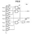
- FIG. 8 An example of the circuit for realizing these logic formulae is shown in Fig. 8.
- This circuit is comprised of seven XOR gates X3 to X9 and two OR gates OR3 and OR4.
- ADB[2] is output from the XOR gate X3 with E[4] and ADB[3] input thereto.
- E[2] and E[4] are input to the XOR gate X4,
- E[6] and ADB[3] are input to the XOR gate X5, and
- ADB[1] is output from the OR gate OR3 with the outputs of the XOR gates X4 and X5 input thereto.
- E[7] and ADB[3] are input to the XOR gate X6, E[3] and E[4] are input to the XOR gate X7.
- E[1] and E[2] are input to the XOR gate X8, E[5] and E[6] are input to the XOR gate X9, and ADB[0] is output from the 4-input OR gate OR4 with the outputs of the XOR gates X6 to X9 input thereto.
- the actual circuit is not a simple combination logic.
- Some latch circuits are appropriately placed in the way of encoding. Namely, as the most significant bit (MSB) described in formula (9-1), as will be mentioned later, F[2] is already existing as it is, but usually a latch stages for delaying the output by exactly the same amount of clocks as the number of stages of the least significant bits is necessary to match the pipeline delay. Similarly, the bits described in formula (9-2), formula (9-3), and further formula (10-1) and formula (10-2) must have the same amount of delay of the least significant bit (LSB), so some latch circuits or delay stages for this purpose become necessary.
- the latch circuits are placed in the circuit 4 or the circuit 5 of Fig. 1 or the comparator blocks 3 -1 to 3 -8 .
- Figure 9 shows an example of the latch circuit.
- the latch circuit of the present example is comprised of a transfer stage and a latch stage.
- the former is comprised of npn transistors Q to Q3.
- the latter is comprised of npn transistors Q5 to Q7.
- the transfer stage is a differential amplifier.
- the base of the npn transistor Q1 is connected to an input terminal Tin of the analog signal Vin, and the collector is connected to a supply line of a power supply voltage V CC via the resistor element R1.
- the base of the npn transistor Q2 is connected to an input terminal T/in of a reference voltage V/in, and the collector is connected to the supply line of the power supply voltage V CC via the resistor element R2. Connection points of the collectors of these npn transistors with the resistor elements form nodes ND1 and ND2.
- the emitters of the npn transistors Q1 and Q2 are commonly connected to the collector of the npn transistor Q3.
- the latch stage is comprised of the npn transistors Q4. Q5, and Q6.
- the base of the npn transistor Q4 is connected to the node ND2, the collector is connected to the node ND1, the base of the npn transistor Q5 is connected to the node ND1, and the collector is connected to the node ND2.
- the emitters of these npn transistors are commonly connected to the collector of the npn transistor Q6.
- the base of the npn transistor Q3 is connected to an input terminal T CLKn of a clock signal CLKN
- the base of the npn transistor Q6 is connected to an input terminal T CLK of a clock signal CLK
- the emitters of these npn transistors are commonly connected to the current source I1.
- the clock signal CLKN is the inverted signal of the clock signal CLK.
- An output circuit of the transfer stage is comprised of the npn transistors Q7and Q8 and current sources I2 and I3.
- the base of the npn transistor Q7 is connected to the node ND1, the collector is connected to the supply line of the power supply voltage V CC , and the emitter is connected to the current source I2.
- the base of the npn transistor Q8 is connected to the node ND2, the collector is connected to the supply line of the power supply voltage V CC , and the emitter is connected to the current source 13.
- the emitter of the npn transistor Q8 is connected to an output terminal Tout of the comparator, and the emitter of the npn transistor Q7 is connected to an inverted output terminal T/out of the comparator.
- a current i 1 of the current source I1 flows through the collector of the npn transistor Q3, the differential amplifier comprised of the npn transistors Q1 and Q2 are active, and the potentials of the collectors of these transistors, that is, the nodes ND1 and ND2, are determined in accordance with the levels of the analog voltage Vin and the reference voltage V/in. For example, when the level of the analog signal Vin is higher than the reference voltage V/in, the node ND1 is a low level, and the node ND2 is a high level. During the period, since the clock signal CLK is low, the current does not flow through the collector of the npn transistor Q6. and the latch stage is not active.
- the difference between the analog signal Vin and the reference voltage V/in is amplified by the differential amplifier and output to the nodes ND1 and ND2.
- the potentials of the nodes ND1 and ND2 are kept by the latch stage.
- the potentials of the nodes ND1 and ND2 are transferred to the output circuit comprised of the npn transistors Q7 and Q8 and the current sources I2 and I3 and output.
- the latch circuit and the output circuit in Fig. 9 are arranged in an output route of the required bits.
- the resistor string 2 was arranged folded by a number of times in accordance with the number of the most significant bits to make it easier to gather the comparators of most significant bits.
- the Gray code is generated at the comparator block 3 -8 of the most significant bits, and Gray-binary conversion is carried out in the first output circuit 4 of the latter stage.
- the circuit to generate the least significant bits from the outputs of the comparator blocks 3 -1 to 3 -7 and the output of the first output circuit 4 is realized by a circuit configuration that does not increase the pipeline delay even if the number of least significant bits is increased.
- the stage number of the XOR gates which has much influence on the pipeline delay, does not increase with the number of least significant bits. Also, the pipeline delay does not increase in accordance with the number of bits as in the Gray-binary conversion circuit in a conventional type ADC.
- the bubble tolerance of the encoding method according to the present embodiment is equivalent to the conventional method of generating all bits by a Gray coding and then converting it to a binary code (hereinafter, referred to as the full bit Gray encoding).
- the AND gates A1 to A7 of the comparator blocks 3 -1 to 3 -8 receive as input two reference voltages apart by at least 8 LSB each other and the comparison results of the input signals, so occurrence of the bubble apart by 8 LSB is rare enough to be negligible in terms of probability.
- the possible bubbles are prevented from becoming a sparkle in the circuit configuration.
- the metastable state tolerance of the encoding method according to the present embodiment is slightly inferior to the full bit Gray encoding in theory.
- the most significant bits are the Gray code per so, so are equivalent, but in the least significant bits, for example E[4] simultaneously appears in the formulae (10-1) to (10-3) of lower significant 3 bits.
- E[4] simultaneously appears in the formulae (10-1) to (10-3) of lower significant 3 bits.
- the metastable state occurring at the time of generation of E[4] exerts an influence upon the lower significant 3 bits.
- the sparkle of this generation mechanism is limited in magnitude thereof to the range of the lower significant bits.
- the stage number of latches up to the stage of the creation of the least significant bits (input stages of formulae (9-1) to (10-3)) can be easily made larger than the conventional ROM type ADC of WOR configuration, so a great improvement can be expected in the sparkle frequency by this.
- the sparkle due to the metastable state is reduced by an exponential function of the stage number of latches up to the latch input of the encoding stage exerting an influence upon the plurality of bits from the comparator output. Accordingly, in the ADC according to the present embodiment, by increasing the stage number of latches, a metastable state tolerance practically the same as that of the conventional method can be guaranteed.
- Fig. 5 to Fig. 8 realize corresponding logic formulae, but if identical logic operation results are obtained, they are not limited to the illustrated circuits.
- the 4-input OR gates OR1 and OR4 in Fig. 5 and Fig. 8 may be realized by for example WOR too.
- the number of folds of the resistor string is not limited to the illustrated one.
- the method of picking up the reference voltages and the arrangement of the comparator blocks can be realized by methods and arrangements other than illustrated.
- the arrangement of the comparator block 3 -8 for creating the higher significant bits on the least significant bit reference voltage VRB side can be easily executed as a modification not accompanied with any other significant change.
- the resistor string is arranged by folding by number of times corresponding to the number of the most significant bits of the output bits.
- comparators of most significant bits are arranged adjacently.
- generation of a Gray code for the most significant bits becomes easier.
- the number of serial stages of the operation elements (XOR gates) of the exclusive OR for the Gray-binary conversion in the first output circuit also becomes small.
- the stage number of XOR gates does not increase by more than one. Accordingly, the increase of the pipeline delay is suppressed to the required lowest limit.
- the resistor string can be arranged at the center portion of the ADC, so a good integral linearity is achieved.
- a flash analog-to-digital converter with a pipeline delay as small as that of the encoding method using a binary code for all bits can be realized while maintaining a good error-rate performance equivalent to that of an encoding method using a full bit Gray encoding.
Landscapes
- Engineering & Computer Science (AREA)
- Theoretical Computer Science (AREA)
- Analogue/Digital Conversion (AREA)
Abstract
Description
Claims (14)
- A flash type analog-to-digital converter comprising a resistor string (2) to generate reference voltages (Vref) when detecting a voltage level of an input signal at the time of conversion of an analog input signal (Vin) to a digital code of predetermined bits, wherein
the resistor string is folded 2n times or a multiple thereof corresponding to a number n of most significant bits when the predetermined bits N are divided to most significant bits and least significant bits. - A flash type analog-to-digital converter as set forth in claim 1, further comprising:a first encoder (3-8) for encoding n bits Gray code; anda second encoder (3-1 - 3-7)for encoding the remaining N-n bit.
- A flash type analog-to-digital converter as set forth in claim 1, further comprising (2N-1) comparators receiving as input the reference voltages different by predetermined voltage steps and the input signal, comparing the input signal with the reference voltages, and creating outputs of logics in accordance with the relative magnitudes,
the (2N-1) comparators being grouped into 2N-n blocks of comparators receiving as input the reference voltages different by increments of 2N-n times the predetermined voltage step and being arranged around the resistor string. - A flash type analog-to-digital converter as set forth in claim 2, whereinsaid first and second encoders have (2N-1) comparators receiving as input the reference voltages different by predetermined voltage steps and the input signal, comparing the input signal with the reference voltages, and creating outputs of logics in accordance with the relative magnitudes, andthe (2N-1) comparators are grouped into 2N-n blocks of comparators receiving as input the reference voltages different by increments of 2N-n times the predetermined voltage step and are arranged around the resistor string.
- A flash type analog-to-digital converter as set forth in claim 4, wherein the first encoder directly converts a thermometer code output by the comparators in the blocks to a Gray code.
- A flash type analog-to-digital converter as set forth in claim 4, wherein the second encoder comprises:a plurality of logic circuits (A1-A4)for detecting state change of logics of (2m-1)th comparator outputs and 2m-th comparator outputs (m: natural number of 2n-1 or less) in the blocks; andan OR gate circuit (OR1) for operating a logical sum of the outputs of the plurality of logic circuits and outputting the same.
- A flash type analog-to-digital converter as set forth in claim 2, further comprising:a first output circuit (4) for converting the Gray code output from the first encoder to a binary code and creating n bits of digital signal; anda second output circuit (5) to generate the remaining bits of digital signal except the n bits among the predetermined bits N by using the digital signal generated by the related first output circuit and the output of the second encoder.
- A flash type analog-to-digital converter as set forth in claim 7, wherein the first output circuit outputs all or part of the n bits earlier than the other bits.
- A flash type analog-to-digital converter as set forth in claim 1, wherein the resistor string is arranged around the center.
- A flash type analog-to-digital converter for generating a plurality of reference voltages different in increments of predetermined voltage steps, comparing the related plurality of reference voltages and an analog input signal in voltage in parallel to detect the voltage level of the analog input signal, and converting the same to a digital code of predetermined bits, comprising:a first encoder (3-8) for encoding most significant n bits of the predetermined bits N and outputting a Gray code;a second encoder (3-1 - 3-7) for encoding the remaining bit among the predetermined bits N and outputting the same;a first output circuit (4) for converting the Gray code output from the first encoder to a binary code and creating n bit of digital code; anda second output circuit (5) for generating the remaining bit of the digital code except the n bits from the predetermined bits N by using the digital code generated by the related first output circuit and the output of the second encoder.
- A flash type analog-to-digital converter as set forth in claim 10. wherein said first and second encoders have (2N-1) comparators receiving as input the reference voltages different by predetermined voltage steps and the input signal, comparing the input signal with the reference voltages, and generating outputs of logics in accordance with the relative magnitudes, and
the (2N-1) comparators are grouped into 2N-n blocks of comparators receiving as input the reference voltages different by increments of 2N-n times the predetermined voltage step. - A flash type analog-to-digital converter as set forth in claim 11, wherein the first encoder directly converts a thermometer code output by the comparators in the blocks to a Gray code.
- A flash type analog-to-digital converter as set forth in claim 11, wherein the second encoder comprises:a plurality of logic circuits (A1-A4) for detecting state change of logics of (2m-1)th comparator outputs and 2m-th comparator outputs (m: natural number of 2n-1 or less) in the blocks; andan OR gate circuit (OR1) for operating a logical sum of the outputs of the plurality of logic circuits and outputting the same.
- A flash type analog-to-digital converter as set forth in claim 10, wherein the first output circuit outputs all or part of the n bits earlier than the other bits.
Applications Claiming Priority (4)
| Application Number | Priority Date | Filing Date | Title |
|---|---|---|---|
| JP2000132863 | 2000-04-27 | ||
| JP2000132863 | 2000-04-27 | ||
| JP2000168691A JP4360010B2 (en) | 2000-04-27 | 2000-06-06 | Parallel type analog-digital converter |
| JP2000168691 | 2000-06-06 |
Publications (3)
| Publication Number | Publication Date |
|---|---|
| EP1150433A2 true EP1150433A2 (en) | 2001-10-31 |
| EP1150433A3 EP1150433A3 (en) | 2004-10-13 |
| EP1150433B1 EP1150433B1 (en) | 2006-11-29 |
Family
ID=26591379
Family Applications (1)
| Application Number | Title | Priority Date | Filing Date |
|---|---|---|---|
| EP01401117A Expired - Lifetime EP1150433B1 (en) | 2000-04-27 | 2001-04-27 | Flash type analog-to-digital converter |
Country Status (4)
| Country | Link |
|---|---|
| US (1) | US6480135B2 (en) |
| EP (1) | EP1150433B1 (en) |
| JP (1) | JP4360010B2 (en) |
| DE (1) | DE60124812T2 (en) |
Families Citing this family (11)
| Publication number | Priority date | Publication date | Assignee | Title |
|---|---|---|---|---|
| SE518900C2 (en) * | 2001-03-26 | 2002-12-03 | Ericsson Telefon Ab L M | Method and apparatus for calibrating bubble / A / D converters |
| JP2003273735A (en) * | 2002-03-12 | 2003-09-26 | Denso Corp | A / D conversion method and device |
| US20050083223A1 (en) * | 2003-10-20 | 2005-04-21 | Devendorf Don C. | Resolution enhanced folding amplifier |
| US20060109156A1 (en) * | 2004-11-19 | 2006-05-25 | Potentia Semiconductor Corporation | Trimming resistance ladders in analog-digital converters |
| US7446690B2 (en) * | 2006-11-06 | 2008-11-04 | Atmel Corporation | Apparatus and method for implementing an analog-to-digital converter in programmable logic devices |
| US7933354B2 (en) * | 2006-11-22 | 2011-04-26 | Semtech Corporation | Encoding and decoding architecture and method for pipelining encoded data or pipelining with a look-ahead strategy |
| KR100851995B1 (en) * | 2007-02-12 | 2008-08-13 | 주식회사 하이닉스반도체 | Receiver circuit |
| US7623051B2 (en) * | 2008-04-29 | 2009-11-24 | Analog Devices, Inc. | Metastability error reduction in signal converter systems |
| US9893737B1 (en) | 2017-01-13 | 2018-02-13 | Apple Inc. | Multi-stage overload protection scheme for pipeline analog-to-digital converters |
| FR3113139B1 (en) | 2020-07-30 | 2022-11-25 | St Microelectronics Rousset | Voltage comparator |
| EP4184794B1 (en) * | 2021-11-23 | 2026-05-06 | Infineon Technologies Austria AG | Analog-to-digital converter and method for analog-to-digital conversion |
Family Cites Families (8)
| Publication number | Priority date | Publication date | Assignee | Title |
|---|---|---|---|---|
| US4276543A (en) | 1979-03-19 | 1981-06-30 | Trw Inc. | Monolithic triple diffusion analog to digital converter |
| US4386339A (en) | 1980-03-31 | 1983-05-31 | Hewlett-Packard Company | Direct flash analog-to-digital converter and method |
| AU557017B2 (en) * | 1981-07-21 | 1986-12-04 | Sony Corporation | Analog-to-digital converter |
| JP2714999B2 (en) * | 1990-11-28 | 1998-02-16 | シャープ株式会社 | Analog / digital converter |
| JP2945805B2 (en) * | 1992-10-01 | 1999-09-06 | 松下電器産業株式会社 | A / D converter |
| US5623265A (en) * | 1994-01-28 | 1997-04-22 | Texas Instruments Incorporated | Flash analog-to-digital converter and method of operation |
| US5644312A (en) * | 1994-11-30 | 1997-07-01 | Analog Devices, Inc. | Rom encoder circuit for flash ADC'S with transistor sizing to prevent sparkle errors |
| US6222476B1 (en) * | 1999-08-30 | 2001-04-24 | Lsi Logic Corporation | Architecture to reduce errors due to metastability in analog to digital converters |
-
2000
- 2000-06-06 JP JP2000168691A patent/JP4360010B2/en not_active Expired - Fee Related
-
2001
- 2001-04-26 US US09/842,061 patent/US6480135B2/en not_active Expired - Lifetime
- 2001-04-27 EP EP01401117A patent/EP1150433B1/en not_active Expired - Lifetime
- 2001-04-27 DE DE60124812T patent/DE60124812T2/en not_active Expired - Lifetime
Also Published As
| Publication number | Publication date |
|---|---|
| US6480135B2 (en) | 2002-11-12 |
| EP1150433A3 (en) | 2004-10-13 |
| EP1150433B1 (en) | 2006-11-29 |
| DE60124812T2 (en) | 2007-10-11 |
| DE60124812D1 (en) | 2007-01-11 |
| JP4360010B2 (en) | 2009-11-11 |
| US20010040523A1 (en) | 2001-11-15 |
| JP2002016497A (en) | 2002-01-18 |
Similar Documents
| Publication | Publication Date | Title |
|---|---|---|
| US7864093B2 (en) | Pulse phase difference detecting circuit and A/D converter using the same | |
| CN106209101B (en) | Analog-digital converter | |
| WO2001047123A1 (en) | High-precision d-a converter circuit | |
| EP1256173A1 (en) | Digital logic correction circuit for a pipeline analog to digital (a/d) converter | |
| US5194867A (en) | Flash analog-to-digital converter employing least significant bit-representative comparative reference voltage | |
| EP1150433B1 (en) | Flash type analog-to-digital converter | |
| JP4263050B2 (en) | Successive approximation type A / D converter | |
| US6388602B1 (en) | Bubble and meta-stability error immune gray-code encoder for high-speed A/D converters | |
| US20010040522A1 (en) | Analog-to-digital converter | |
| JP4526919B2 (en) | A / D converter | |
| JP2013187695A (en) | Comparator and ad converter | |
| US7403149B2 (en) | Folding and interpolating analog-to-digital converter and method of converting analog signal to digital signal | |
| JP2816354B2 (en) | Electronic circuit for synchronizing bit transitions in digital codes | |
| KR100691347B1 (en) | Bubble Error Canceling Device, Analog-to-Digital Converter and Bubble Error Cancellation Method | |
| EP0328215B1 (en) | Error correction circuit suitable for thermometer or circular code | |
| JP3339566B2 (en) | Thermometric-to-binary code conversion method and circuit, and encoder element circuit used therefor | |
| US8035543B2 (en) | Analog-to-digital conversion circuit | |
| JP2009278634A (en) | Flash type analog-to-digital converter | |
| EP4184794B1 (en) | Analog-to-digital converter and method for analog-to-digital conversion | |
| JP2010004422A (en) | D/a conversion circuit | |
| KR100620986B1 (en) | Beat converter circuit of AD converter | |
| JPH06291660A (en) | A / D converter | |
| Mortazavi et al. | A New folding & interpolating ADC structure with reduced DNL/INL | |
| EP0586546A4 (en) | Flash analog-to-digital converter. | |
| JPH0969780A (en) | Analog-digital converter |
Legal Events
| Date | Code | Title | Description |
|---|---|---|---|
| PUAI | Public reference made under article 153(3) epc to a published international application that has entered the european phase |
Free format text: ORIGINAL CODE: 0009012 |
|
| AK | Designated contracting states |
Kind code of ref document: A2 Designated state(s): AT BE CH CY DE DK ES FI FR GB GR IE IT LI LU MC NL PT SE TR |
|
| AX | Request for extension of the european patent |
Free format text: AL;LT;LV;MK;RO;SI |
|
| PUAL | Search report despatched |
Free format text: ORIGINAL CODE: 0009013 |
|
| AK | Designated contracting states |
Kind code of ref document: A3 Designated state(s): AT BE CH CY DE DK ES FI FR GB GR IE IT LI LU MC NL PT SE TR |
|
| AX | Request for extension of the european patent |
Extension state: AL LT LV MK RO SI |
|
| 17P | Request for examination filed |
Effective date: 20050125 |
|
| AKX | Designation fees paid |
Designated state(s): DE FR GB |
|
| GRAP | Despatch of communication of intention to grant a patent |
Free format text: ORIGINAL CODE: EPIDOSNIGR1 |
|
| GRAS | Grant fee paid |
Free format text: ORIGINAL CODE: EPIDOSNIGR3 |
|
| GRAA | (expected) grant |
Free format text: ORIGINAL CODE: 0009210 |
|
| AK | Designated contracting states |
Kind code of ref document: B1 Designated state(s): DE FR GB |
|
| REG | Reference to a national code |
Ref country code: GB Ref legal event code: FG4D |
|
| REF | Corresponds to: |
Ref document number: 60124812 Country of ref document: DE Date of ref document: 20070111 Kind code of ref document: P |
|
| ET | Fr: translation filed | ||
| PLBE | No opposition filed within time limit |
Free format text: ORIGINAL CODE: 0009261 |
|
| STAA | Information on the status of an ep patent application or granted ep patent |
Free format text: STATUS: NO OPPOSITION FILED WITHIN TIME LIMIT |
|
| 26N | No opposition filed |
Effective date: 20070830 |
|
| REG | Reference to a national code |
Ref country code: GB Ref legal event code: 746 Effective date: 20120702 |
|
| REG | Reference to a national code |
Ref country code: DE Ref legal event code: R084 Ref document number: 60124812 Country of ref document: DE Effective date: 20120614 |
|
| PGFP | Annual fee paid to national office [announced via postgrant information from national office to epo] |
Ref country code: GB Payment date: 20140422 Year of fee payment: 14 |
|
| PGFP | Annual fee paid to national office [announced via postgrant information from national office to epo] |
Ref country code: FR Payment date: 20140422 Year of fee payment: 14 Ref country code: DE Payment date: 20140418 Year of fee payment: 14 |
|
| REG | Reference to a national code |
Ref country code: DE Ref legal event code: R119 Ref document number: 60124812 Country of ref document: DE |
|
| GBPC | Gb: european patent ceased through non-payment of renewal fee |
Effective date: 20150427 |
|
| PG25 | Lapsed in a contracting state [announced via postgrant information from national office to epo] |
Ref country code: GB Free format text: LAPSE BECAUSE OF NON-PAYMENT OF DUE FEES Effective date: 20150427 Ref country code: DE Free format text: LAPSE BECAUSE OF NON-PAYMENT OF DUE FEES Effective date: 20151103 |
|
| REG | Reference to a national code |
Ref country code: FR Ref legal event code: ST Effective date: 20151231 |
|
| PG25 | Lapsed in a contracting state [announced via postgrant information from national office to epo] |
Ref country code: FR Free format text: LAPSE BECAUSE OF NON-PAYMENT OF DUE FEES Effective date: 20150430 |