EP1150358A1 - Optical module - Google Patents
Optical module Download PDFInfo
- Publication number
- EP1150358A1 EP1150358A1 EP00966424A EP00966424A EP1150358A1 EP 1150358 A1 EP1150358 A1 EP 1150358A1 EP 00966424 A EP00966424 A EP 00966424A EP 00966424 A EP00966424 A EP 00966424A EP 1150358 A1 EP1150358 A1 EP 1150358A1
- Authority
- EP
- European Patent Office
- Prior art keywords
- photodetector
- light emitting
- optical module
- emitting device
- conductor wall
- Prior art date
- Legal status (The legal status is an assumption and is not a legal conclusion. Google has not performed a legal analysis and makes no representation as to the accuracy of the status listed.)
- Withdrawn
Links
Images





Classifications
-
- H—ELECTRICITY
- H10—SEMICONDUCTOR DEVICES; ELECTRIC SOLID-STATE DEVICES NOT OTHERWISE PROVIDED FOR
- H10F—INORGANIC SEMICONDUCTOR DEVICES SENSITIVE TO INFRARED RADIATION, LIGHT, ELECTROMAGNETIC RADIATION OF SHORTER WAVELENGTH OR CORPUSCULAR RADIATION
- H10F55/00—Radiation-sensitive semiconductor devices covered by groups H10F10/00, H10F19/00 or H10F30/00 being structurally associated with electric light sources and electrically or optically coupled thereto
- H10F55/20—Radiation-sensitive semiconductor devices covered by groups H10F10/00, H10F19/00 or H10F30/00 being structurally associated with electric light sources and electrically or optically coupled thereto wherein the electric light source controls the radiation-sensitive semiconductor devices, e.g. optocouplers
- H10F55/205—Radiation-sensitive semiconductor devices covered by groups H10F10/00, H10F19/00 or H10F30/00 being structurally associated with electric light sources and electrically or optically coupled thereto wherein the electric light source controls the radiation-sensitive semiconductor devices, e.g. optocouplers wherein the radiation-sensitive semiconductor devices have no potential barriers, e.g. photoresistors
- H10F55/207—Radiation-sensitive semiconductor devices covered by groups H10F10/00, H10F19/00 or H10F30/00 being structurally associated with electric light sources and electrically or optically coupled thereto wherein the electric light source controls the radiation-sensitive semiconductor devices, e.g. optocouplers wherein the radiation-sensitive semiconductor devices have no potential barriers, e.g. photoresistors wherein the electric light source comprises semiconductor devices having potential barriers, e.g. light emitting diodes
-
- G—PHYSICS
- G02—OPTICS
- G02B—OPTICAL ELEMENTS, SYSTEMS OR APPARATUS
- G02B6/00—Light guides; Structural details of arrangements comprising light guides and other optical elements, e.g. couplings
- G02B6/24—Coupling light guides
- G02B6/42—Coupling light guides with opto-electronic elements
- G02B6/4201—Packages, e.g. shape, construction, internal or external details
- G02B6/4274—Electrical aspects
- G02B6/4277—Protection against electromagnetic interference [EMI], e.g. shielding means
-
- G—PHYSICS
- G02—OPTICS
- G02B—OPTICAL ELEMENTS, SYSTEMS OR APPARATUS
- G02B6/00—Light guides; Structural details of arrangements comprising light guides and other optical elements, e.g. couplings
- G02B6/24—Coupling light guides
- G02B6/42—Coupling light guides with opto-electronic elements
- G02B6/4201—Packages, e.g. shape, construction, internal or external details
- G02B6/4256—Details of housings
- G02B6/4262—Details of housings characterised by the shape of the housing
- G02B6/4265—Details of housings characterised by the shape of the housing of the Butterfly or dual inline package [DIP] type
-
- H—ELECTRICITY
- H10—SEMICONDUCTOR DEVICES; ELECTRIC SOLID-STATE DEVICES NOT OTHERWISE PROVIDED FOR
- H10W—GENERIC PACKAGES, INTERCONNECTIONS, CONNECTORS OR OTHER CONSTRUCTIONAL DETAILS OF DEVICES COVERED BY CLASS H10
- H10W90/00—Package configurations
- H10W90/701—Package configurations characterised by the relative positions of pads or connectors relative to package parts
- H10W90/751—Package configurations characterised by the relative positions of pads or connectors relative to package parts of bond wires
- H10W90/754—Package configurations characterised by the relative positions of pads or connectors relative to package parts of bond wires between a chip and a stacked insulating package substrate, interposer or RDL
Definitions
- the present invention relates to an optical module having a substrate on which a light emitting device and a photodetector are mounted.
- bidirectional optical transmission module with a light emitting device and a photodetector incorporated inside is used.
- a reduction in the size and cost of bidirectional optical transmission modules has been demanded since the module has come to be installed domestically.
- a method wherein a part in which a substrate with conductor inter connection laid as necessary is used and a light emitting device and a photodetector are mounted on the substrate is incorporated into a package and connected to optical fibers for transmission and waveguide parts, is suitable in terms of the manufacturing and assembling processes.
- an Si substrate is preferable as the substrate to be provided with a light emitting device and a photodetector. It is possible to acquire a Si material with stable quality at a low price, and the Si material is excellent in workability, so that formation of alignment marks for positioning a light emitting device and a photodetector when mounting them and formation of V-grooves for positioning optical fibers are easy.
- an Si substrate to be used for such a purpose or an Si substrate which has a light emitting device and a photodetector and conductor inter connection provided on it and has alignment marks and V-grooves for positioning formed as necessary is called an SOB (Silicon Optical Bench) according to necessity.
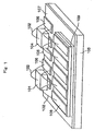
- Fig. 1 shows a conception diagram of the SOB.
- the reference numeral 105 denotes a substrate with a thickness of, for example, 1mm, on which conductor (inter connection) patterns 106 are formed via insulation layer 107 made from SiO 2 or the like.
- Light emitting device 104 and photodetector 101 are mounted on the substrate 105, and connected to the conductor patterns 106 on the substrate 105 by soldering and bonding wires 102. Furthermore, the reference numeral 108 denotes a leader inter connection conductor, and the reference numeral 109 denotes a dielectric.
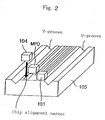
- Fig. 2 is a drawing showing the entire construction of the SOB.
- a photodetector (MPD) for detecting and controlling the output of the light emitting device 104 is disposed at the rear stage of the light emitting device 104.
- an alignment mark for positioning and mounting the light emitting device 104 and photodetector 101, and V-grooves to be used for positioning and connecting the SOB to external optical fibers (ferrules) and waveguides are formed.
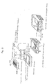
- the SOB thus constructed is packaged together with a connection structure for connection with external optical fibers, for example, preamplifiers, external connection terminals, or optical ferrules as necessary, and is thus completed as an optical module (see Fig. 3).
- external optical fibers for example, preamplifiers, external connection terminals, or optical ferrules as necessary
- the size of the substrate on which the light emitting device and the photodetector are mounted is reduced.
- the current standard pitch of an optical fiber ribbon is 250 ⁇ m, and if connection with the optical fiber ribbon is set as a precondition, it can be said that the application of the module in which the light emitting device and the photodetector are arranged at a 250 ⁇ m pitch is most ideal.
- the light emitting device is driven by a current of 10mA or more, and on the other hand, a photocurrent generated from the photodetector is smaller by several digits than the drive current, which is normally in the order of ⁇ A at most.
- a photocurrent generated from the photodetector is smaller by several digits than the drive current, which is normally in the order of ⁇ A at most.
- the present inventors have come to recognize, in examination of reduction in the size of a module and photodetector's detection of a small photocurrent, that an extremely important factor in the development of an application, in which the light emitting device and photodetector are mounted on an Si substrate, is to solve the problem of electric crosstalk generated by signals of the light emitting device side to influence the photodetector side.
- the present invention provides an optical module wherein the size thereof is reduced and the problem of crosstalk is solved.
- the optical module of the invention has a substrate which has a photodetector and a light emitting device mounted on it and is provided with a conductor wall between the photodetector and the light emitting device.
- the conductor wall is fitted and fixed, as necessary, into a groove portion formed in the substrate.
- the conductor wall is provided with a top plate positioned above one or both of the photodetector and the light emitting device.
- the conductor wall may be formed so as to have a T-shaped section or an L-shaped section.
- the conductor wall may be composed of a first portion formed to have an L-shaped section as mentioned above and a second portion forming a top plate which has a bar-shaped section and is provided independently from said first portion.
- the conductor wall is connected to at least one of a ground provided in a drive circuit of the light emitting device and a .ground provided in an amplifier circuit for electric signals outputted from the photodetector.
- the conductor wall may be formed of a plurality conductors which are independent and separate from each other, and the grounds of each conductor may be separately provided.
- Another embodiment of the conductor wall of the invention may be formed by forming a conductive film on the surface of a wall member made of a resin mold.
- Electric crosstalk is considered to occur through the photodetectors and light emitting device themselves, substrate, inter connection patterns, and bonding wires or the like, and its mechanism is complicated, however, as in the abovementioned construction, electric crosstalk through the light emitting device can be effectively suppressed by forming the conductor wall between the photodetector and the light emitting device.
- the present invention achieves the object of solving the problem of electric crosstalk from signals of the light emitting device side which harmfully influences the photodetector side by a extremely simple construction in which a conductor wall is formed between the photodetector and the light emitting device.
- the optical module of the invention can be said to be excellent for practical use since an effect of remarkably reduced crosstalk-can be obtained by a means without disadvantages such as significant increases in the material cost, the number of processes, and the substrate's size, and substantial deterioration in the characteristics of the optical module.
- the invention is to be applied to an optical module, and is useful for an optical module in which -20dBm is required as the minimum photosensitivity of said photodetector, a normal drive current of said light emitting device is 5mA or more, and the photodetector and the light emitting device which are in the most proximity to each other are disposed at a pitch of 1mm or less (the pitch means the distance between the centers of the light emitting device and photodetector).
- the present invention aims to effectively suppress crosstalk from the light emitting device to the photodetector by employing a means which can be easily employed industrially without complicated processing, an increase in the material cost, and harmful influences on the characteristics of the optical module, and the invention is useful in various industrial fields for manufacturing and using optical modules having substrates on which light emitting devices and photodetectors are mounted.
- the conductor wall is provided with a top plate to cover the photodetector, whereby the electromagnetic shield effect can be increased.
- a construction is employed in which the conductor wall is further provided with a top plate to cover the light emitting device, whereby the electromagnetic effect can be further increased.
- the conductor wall having the top plates is constructed so as to have a T-shaped section or an L-shaped section, or is composed of a first portion formed to have an L-shaped section and the second portion formed to have a bar-shaped section and provided independently from said first portion.
- the optical module is an optical part having at least a photodetector and a light emitting device on one side surface, and substantially consists of an Si substrate as a main body which has the photodetector and the light emitting device mounted on it.
- the optical module is an optical part including a substrate as one component which has the photodetector and the light emitting device mounted on it, that is, an optical part including, as other components, an optical connection mechanism such as an MT connector and a ferrule for connecting the photodetector and light emitting device to optical fibers or waveguides, and/or inter connection and terminals for detecting and amplifying the photocurrent of the photodetector and applying and detecting the drive voltage of the light emitting device, and/or a casing, and/or optical fibers.
- an optical connection mechanism such as an MT connector and a ferrule for connecting the photodetector and light emitting device to optical fibers or waveguides
- inter connection and terminals for detecting and amplifying the photocurrent of the photodetector and applying and detecting the drive voltage of the light emitting device, and/or a casing, and/or optical fibers.
- Fig. 1 is a conception diagram of a conventional SOB
- Fig. 2 is a conceptual diagram of the same conventional SOB
- Fig. 3 is an entire view of a general SOB
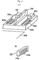
- Figs. 4 are an explanatory views showing an embodiment of the invention, wherein Fig. 4 (a) is a drawing showing the main construction, and Fig. 4 (b) is a drawing showing an example of the conductor wall.
- Fig. 5 is an explanatory view showing another embodiment of the invention
- Fig. 6 is an explanatory view showing still another embodiment of the invention
- Fig. 7 is an explanatory view showing still another embodiment of the invention
- Fig. 8 is an explanatory view showing still another embodiment of the invention
- Fig. 9 is an explanatory view showing.
- Fig. 10 is an explanatory view showing a first detailed example of the invention
- Fig. 11 is an explanatory view showing a second detailed example of the invention
- Fig. 12 is an explanatory view of the results of experiment showing the effect of the invention
- Fig. 13 is an explanatory view of the results of simulation showing the effect of the invention
- Figs. 14 are an explanatory views showing still another embodiment of the invention, wherein Fig. 14(a) is a perspective view, and Fig. 14(b) is a partial enlarged side view.
- conductor wall 219 is mounted between photodetector 201 and light emitting device 204 on Si substrate 205, and shields electromagnetic fields generated by the light emitting device 204.
- the material for the conductor wall 219 is not especially limited as long as the material has excellent conductivity.
- general conductor materials such as copper, aluminum, gold, silver or the like can be used, or other materials, alloy conductor materials, and organic or inorganic conductive materials can be used as long as they have excellent conductivity, their shape is easily processed, and they can be mounted on the Si substrate.
- the conductor wall may have the form of a plate (foil-form) or the form of a mesh (net-form).
- the conductor wall 219 may have conductive film 219b of Cu, Cu/Ni, or Cu/Ni/Au deposited by means of plating on the surface of wall member 219a made of a hard resin mold.
- the conductive film 219b can be formed to be a desired pattern, so that a desirable conduction performance can be obtained and freedom in the module design increases, and therefore, this construction is preferable.
- the height of the conductor wall 219 is formed to be higher than that of the photodetector 201 or light emitting element 204, and in a case where wire bonding 202 is applied on the Si substrate 205 with the photodetector 201 and the light emitting device 204 mounted on it, it is preferable that the height of the conductor wall 219 is made equivalent to or higher than that of the wire bonding 202, and typically, it is preferable that the height of the wall is set to approximately 0.5mm to 1.5mm from the surface of the Si substrate 205.
- a constant electromagnetic shield effect can be obtained even when the conductor wall 219 is formed only in the proximity of the mounted portion of the photodetector 201 at which high photosensitivity is required.
- inter connection patterns 206 and bonding wires 202 for supplying a drive current to the light emitting device 204 and taking-out a signal current detected by the photodetector 201 are laid on the Si substrate 205. Therefore, in order to prevent crosstalk between the patterns and wires, as shown in Fig.
- the conductor wall 219 is disposed on the Si substrate 205 so as to substantially divide the area, in which the photodetector 201, the inter connection pattern 206 for detecting signals received by the photodetector, and the bonding wire 202 are disposed, and the area, in which the light emitting device 204, the inter connection pattern 206 for applying a drive voltage to the device, and the bonding wire 202 are disposed.
- the conductor wall 219 is installed across the entire length of the Si substrate 205 to completely divide the abovementioned areas on the Si substrate 205.
- the conductor wall 219 can be installed and fixed by using an adhesive such as an epoxy resin, however, as shown in Fig. 5, groove 220 is formed at the position for installation of the conductor wall 219 on the Si substrate 205, and the conductor wall 219 can be fitted and fixed into the groove 220.
- the groove 220 can be formed by means of a generally-known method, for example, etching or dicing, and the provision of the groove has advantages such as a higher fixing strength and a higher shield effect of the conductor wall 219. Needless to say, use of an adhesive to secure the fixation is preferable even when the conductor wall 219 is fitted and fixed into the groove 220.
- conductor pattern 221 is formed on the Si substrate 205, and the conductor wall 219 is installed on this conductor pattern 221.
- the conductor pattern 221 can be used as a positioning mark for the conductor wall 219, and any method such as ultrasonic connection or soldering can be employed as a method of fixing the conductor wall 219, and since this conductor pattern 221 functions as a protection trace, the shield effect further increases.
- the conductor wall 219 is not directly adhered and fixed on the Si substrate 205, but is fixed to a ferrule, lead frame, or the inner wall of a casing of the optical module, and when the Si substrate 205, and the ferrule, lead frame, or casing are installed in the module in the assembly process of the optical module, the conductor wall 219 fixed to the ferrule or the like is disposed between the photodetector 201 and light emitting device 204 on the Si substrate 205. If the space between the photodetector 201 and the light emitting device 204 becomes narrower, fixation of the conductor wall 219 onto the Si substrate 205 becomes difficult. However, this method has an advantage such that the installing operation of the conductor wall 219 can be made easier.
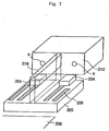
- Fig. 7 shows the positioning relationship between ferrule 212 to which the conductor wall 219 is fixed and Si substrate 205. Since there is a necessity to align optical fibers and the photodetector 201 and light emitting device 204, the Si substrate 205 and the ferrule 212 are to be relatively positioned by using the V-groove, and therefore, a method wherein the conductor wall 219 is attached to the ferrule 212 in advance is especially convenient. "A" in the same figure show optical fiber insertion holes.
- the light emitting device 204 is molded by using a resin sealant or the like, and a conductive material layer is formed.on the molded surface, whereby the conductor wall 219 is formed.
- the photodetector 201 is molded by using a resin sealant or the like, and the conductor wall consisting of a conductive material layer can be formed on the molded surface.
- the conductive material layer can be formed by spattering or plating metal or coating a conductive composition (a conductive resin or a conductive coating).
- masking becomes necessary for the photodetector 201 or the conductor pattern 206 around the light emitting device 204.
- the photodetector 201 is molded in the same manner as the light emitting device 204, and a conductive material layer is formed on both of the molded surfaces of the photodetector and the light emitting device, masking may be omitted.
- the electromagnetic shield effect can be further increased by also grounding the protection trace 221.
- the conductor wall 219 is provided with top plate 222 covering the photodetector 201, whereby the electromagnetic shield effect can be further increased. Furthermore, the conductor wall 219 is provided with top plate 222 to cover the light emitting device 204, whereby the electromagnetic shield effect can be still further increased.
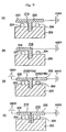
- the form of the conductor wall 219 may have a T-shaped section (see Fig. 9(a)) or L-shaped section (see Fig. 9(b)), may be composed of first portion 219a formed to have an L-shaped section as mentioned above and second portion 219b which is provided independently and separately from said first portion and has a bar-shaped section (see Fig. 9(c)), or may be constructed so that two portions with L-shaped sections are formed back to back with each other to cover the photodetector 201 and the light emitting device 204 (see Fig. 9(d)).
- the conductor wall having an L-shaped section is easily obtained by bending one plate member.
- the conductor wall having a T-shaped section is obtained by adhering and fixing two plate members with an electric conductive adhesive or by means of soldering.
- the second portion 219b of the form with a bar-shaped section is positioned and fixed by being attached to a casing of the module.
- the conductor 219 is connected to at least one of a ground provided in the drive circuit of the light emitting device 204 and a ground provided in the amplification circuit of electric signals outputted from the photodetector. In this construction, additional provision of ground terminals is unnecessary, and the inter connection patterns are short and simple, so that the optical module can be easily reduced in size.
- the ground GND1 of the first portion 219a which is formed so as to have an L-shaped section of the conductor wall 219 and provided at the photodetector 201 side is also used as a ground of the amplification circuit of electric signals outputted from the photodetector
- the ground GND2 of the second portion 219b of the conductor wall 219 which is formed so as to have a bar-shaped section and provided at the light emitting device 204 side is also used as a ground of the drive circuit of the light emitting device 204.
- the conductor wall 219 is formed of a plurality of portions provided independently and separately from each other, by independently and separately providing grounds for the respective conductor portions 219a and 219b within the SOB, the amount of crosstalk can be reduced, and the inter connection patterns can be constructed to be short and simple.
- Fig. 9(b) and Fig. 9(c) needless to say, it is also possible to construct the conductor 219 or 219a having an L-shaped section so as to cover the light emitting device 204 side.
- Fig. 10 is a schematic view showing a first concrete example of the optical module of the invention.
- the reference numeral 205 denotes an Si substrate having a thickness of 1mm, a specific resistance of 2000 ⁇ cm, and a size of 3x3mm on which the photodetector 201 and the light emitting device 204 are mounted.
- SiO 2 insulation film 207 on the surface of the Si substrate 205 is formed by means of the thermal oxidation method
- copper or gold inter connection patterns 206a and 206b on the SiO 2 insulation film 207 are formed by means of depositing and the generally known lift-off method using photolithography.
- the light emitting device 201 and photodetector 204 are positioned by using these inter connection patterns 206a and 206b as alignment marks, and fixed by means of soldering.
- Conductor wall 219 is installed between the light emitting device 201 and the photodetector 204 for the purpose of the suppression of electric crosstalk.
- the conductor wall 219 is formed of a copper plate cut-out so as to have a thickness of 0.15mm and a size of 1.5x5mm, which is fixed on the Si substrate 205 by using an epoxy adhesive.
- a conductor wall having an I-shaped section is employed as the conductor wall 219.
- the photodetector 201 and conductor pattern 206a for taking-out the photocurrent from the photodetector 201; and the light emitting device 204 and conductor pattern 206b for driving the light emitting device 204 are divided and disposed at both sides of the conductor wall 219 so as to sandwich the conductor wall 219 between them.
- the same V-groove as that of Fig. 2 is formed in the Si substrate 205 for the purpose of alignment with and connection to external optical fibers, and in the same manner as that of the module shown in Fig. 2, a photodetector (MPD in Fig. 2) for detecting the output of the light emitting device 204 and feedback-control is mounted at the rear stage of the light emitting device 204, however, its illustration is omitted for convenience when drawing the figure.
- a generally-known edge emission type light emitting device which has a resonator formed of an InGaAsP active layer with a double hetero structure on an InP substrate, and has an oscillation wavelength of 1.31 ⁇ m and a threshold current of 5mA.
- an edge illumination type photodetector is employed, which has an InGaAsP waveguide type light absorbing layer on an InP substrate, and has a photosensitivity of 0.8A/W.
- both devices 201 and 204 are installed at the end part of the Si substrate 205 so that the light emission direction and light incidence direction of both devices 201 and 204 are coupled with those of the optical fibers 211 as shown in Fig. 10.
- lead frame 213 composes a part of the external form of the optical module, which is provided with, in addition to the Si substrate 205 with the photodetector 201 the light emitting device 204 mounted on it, bias and output terminals 215 and 216 for taking-out a detected current from the photodetector 201, positive and negative terminals 217 and 218 for supplying a drive current to the light emitting device 204, and earthing terminal 214. Furthermore, optical ferrule 212 for connection to the optical fibers 211 is attached.
- preamplifier 203 On the lead frame 213, preamplifier 203 is attached which amplifies a detection signal from the photodetector 201 and transmits the signal to the outside of the optical module, and components and inter connection patterns on the Si substrate 205, or terminals and preamplifier 203 on the lead frame 213 are connected by bonding wires 202 as necessary.
- the materials and forms of the lead frame and the terminals or the optical ferrule are designed upon taking the strength, reliability, and convenience for connection to external parts of the optical module into consideration, however, these are not provided as indispensable conditions of the invention, so that detailed description thereof is omitted.
- the conductor wall 219 provided on the Si substrate 205 is connected to the earthing terminal 214 via the bonding wire 202.
- Fig. 11 is an explanatory view showing a second concrete example of the invention.
- the second concrete example of the invention is different from the first concrete example in the point that a part of the conductor wall 219 is installed in a manner causing it to fit into groove 220 formed in the Si substrate 205.
- the groove 220 in the second concrete example is formed by etching after forming the SiO 2 insulation film 207, and is formed to have a width of 0.20mm and a depth of 0.5mm across the entire length of the Si substrate 205.
- a copper plate with a thickness 0.15mm and a size of 2x5mm is used for the conductor wall 219, and the conductor wall 219 is installed so as to be 1.5mm higher than the surface of the Si substrate 205 as in concrete example 1.
- FIG. 12 For confirmation of the effect of the invention, the results of comparative measurements are shown in Fig. 12.
- A shows the amount of crosstalk in the optical module of concrete example 1
- B shows the amount of crosstalk in the optical module of concrete example 2.
- C in the figure shows the results of measurements of the amount of crosstalk in a condition where the conductor wall 219 and the bonding wire 202 which had connected the conductor wall to the earthing terminal 214 have been removed from the optical module of concrete example 1.
- Fig. 4(a) I-shaped conductor wall
- Fig. 9(a) T-shaped conductor wall
- Fig. 9(b) L-shaped conductor wall
- Fig. 9(c) L- and bar-shaped conductor wall
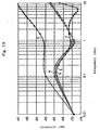
- the characteristic lines a, b, and c of Fig. 13 show the characteristics of the respective optical modules of Fig. 9(a), Fig. 9(b), and Fig. 9(c).
- the result of simulation in the case where the width of the conductor wall 219 (the width in the direction connecting the light emitting device 204 and the photodetector 201) is set to 200 ⁇ m is shown by the characteristic line d of Fig. 13, and the result of simulation in the case where the width of the conductor wall 219 is set to 350 ⁇ m is shown by the characteristic line e of the same figure.
- the width of the conductor wall 219 is set to 200 ⁇ m
- the amount of crosstalk in the case where the width is set to 350 ⁇ m is still less than in the above case, so that it can be understood that an increase in width of the conductor wall 219 is an effective means for suppressing the amount of crosstalk.
- the width of the conductor wall 219 is set to 300 ⁇ m or more.
- the obtained electromagnetic shield effect at a frequency of 1GHz or more is greater than that of the other cases.
- the conductor wall 219 is provided only for division on the Si substrate in the abovementioned embodiments and examples, however, a more preferable embodiment is as shown in Figs. 14(a) and (b) in which the conductor wall 219 is extended so as to also divide the wires and terminals to be connected to the Si substrate 205 between the photodetector side and the light emitting device side.
- the optical module which has an end face incidence type photodetector and an end face emission type light emitting device mounted on the Si substrate is described above as an embodiment, however, the invention is applicable to an optical module using a surface light emitting device and a surface photodetector, wherein the same crosstalk reduction effect can be obtained.
- an optical module having one photodetector and one light emitting device mounted on an Si substrate is mainly described, however, the invention is applicable to an optical module having a plurality of photodetectors and a plurality of light emitting devices mounted on an Si substrate.
- the construction of the invention it is required that at least one conductor wall is provided between the photodetectors and the light emitting devices.
- an optical module in which the optical devices are directly connected to optical fibers is mainly described, however, the invention is applicable to various optical modules, for example, an optical module in which planar waveguides (PLC) are mounted on an substrate as well as a photodetector and a light emitting device, and the devices are connected to optical fibers via said waveguides.
- PLC planar waveguides
- the optical module of the invention is a module having a photodetector and a light emitting device mounted on a substrate, which is suitable for optical transmission since high quality signal processing can be performed by suppressing the influence of crosstalk on the photodetector from the light emitting device side and detecting a extremely small photocurrent of the photodetector in the module.
Landscapes
- Physics & Mathematics (AREA)
- Electromagnetism (AREA)
- General Physics & Mathematics (AREA)
- Optics & Photonics (AREA)
- Optical Couplings Of Light Guides (AREA)
- Light Receiving Elements (AREA)
- Semiconductor Lasers (AREA)
- Photo Coupler, Interrupter, Optical-To-Optical Conversion Devices (AREA)
Abstract
The present invention provides an optical module in which
a photodetector and a light emitting device are arranged at
a narrow pitch on an Si substrate and high receiving sensitivity
of the photodetector is realized, and the optical module of
the invention suppresses the influences of electromagnetic
fields on the photodetector, which are generated by the light
emitting device. A conductor wall (219) is provided between
the photodetector (201) and the light emitting device (204)
arranged on the Si substrate.
Description
The present invention relates to an optical module having
a substrate on which a light emitting device and a photodetector
are mounted.
For example, in an optical transmission system with the
function of bidirectional transmission, a bidirectional
optical transmission module with a light emitting device and
a photodetector incorporated inside is used. According to
recent developments in computer hardware and networks, a
reduction in the size and cost of bidirectional optical
transmission modules has been demanded since the module has
come to be installed domestically.
For reduction in the size and cost, a method, wherein a
part in which a substrate with conductor inter connection laid
as necessary is used and a light emitting device and a
photodetector are mounted on the substrate is incorporated into
a package and connected to optical fibers for transmission and
waveguide parts, is suitable in terms of the manufacturing and
assembling processes.
In this case, an Si substrate is preferable as the substrate
to be provided with a light emitting device and a photodetector.
It is possible to acquire a Si material with stable quality
at a low price, and the Si material is excellent in workability,
so that formation of alignment marks for positioning a light
emitting device and a photodetector when mounting them and
formation of V-grooves for positioning optical fibers are easy.
In the present specification, an Si substrate to be used
for such a purpose or an Si substrate which has a light emitting
device and a photodetector and conductor inter connection
provided on it and has alignment marks and V-grooves for
positioning formed as necessary is called an SOB (Silicon
Optical Bench) according to necessity.
Fig. 1 shows a conception diagram of the SOB. Referencing
to the figure, the reference numeral 105 denotes a substrate
with a thickness of, for example, 1mm, on which conductor (inter
connection) patterns 106 are formed via insulation layer 107
made from SiO2 or the like.
Fig. 2 is a drawing showing the entire construction of the
SOB. In this figure, in addition to the light emitting device
(LD) 104 and the photodetector (PD) 101, a photodetector (MPD)
for detecting and controlling the output of the light emitting
device 104 is disposed at the rear stage of the light emitting
device 104. On the substrate 105, an alignment mark for
positioning and mounting the light emitting device 104 and
photodetector 101, and V-grooves to be used for positioning
and connecting the SOB to external optical fibers (ferrules)
and waveguides are formed.
The SOB thus constructed is packaged together with a
connection structure for connection with external optical
fibers, for example, preamplifiers, external connection
terminals, or optical ferrules as necessary, and is thus
completed as an optical module (see Fig. 3).
For realizing reduction in the size of the optical module,
it is preferable that the size of the substrate on which the
light emitting device and the photodetector are mounted is
reduced. For example, the current standard pitch of an optical
fiber ribbon is 250µm, and if connection with the optical fiber
ribbon is set as a precondition, it can be said that the
application of the module in which the light emitting device
and the photodetector are arranged at a 250µm pitch is most
ideal.
Furthermore, generally, the light emitting device is
driven by a current of 10mA or more, and on the other hand,
a photocurrent generated from the photodetector is smaller by
several digits than the drive current, which is normally in
the order of µA at most. Particularly, in optical transmission,
since it is demanded that the relay stations be reduced and
transmission be made with more receiving stations, it is
important to increase the photosensitivity of the
photodetector. For example, in a certain standard, a minimum
receiving sensitivity of -30dBm (0.001mW) or less is required
for an application of several-hundred Mb/s, and also, some
cases require detection of a photocurrent of µA or less.
The present inventors have come to recognize, in
examination of reduction in the size of a module and
photodetector's detection of a small photocurrent, that an
extremely important factor in the development of an application,
in which the light emitting device and photodetector are
mounted on an Si substrate, is to solve the problem of electric
crosstalk generated by signals of the light emitting device
side to influence the photodetector side. The present invention
provides an optical module wherein the size thereof is reduced
and the problem of crosstalk is solved.
The present invention provides an optical module having
the following construction. That is, the optical module of the
invention has a substrate which has a photodetector and a light
emitting device mounted on it and is provided with a conductor
wall between the photodetector and the light emitting device.
The conductor wall is fitted and fixed, as necessary, into a
groove portion formed in the substrate.
In a more preferable embodiment, the conductor wall is
provided with a top plate positioned above one or both of the
photodetector and the light emitting device. The conductor wall
may be formed so as to have a T-shaped section or an L-shaped
section. As another embodiment, the conductor wall may be
composed of a first portion formed to have an L-shaped section
as mentioned above and a second portion forming a top plate
which has a bar-shaped section and is provided independently
from said first portion.
In a preferable example, the conductor wall is connected
to at least one of a ground provided in a drive circuit of the
light emitting device and a .ground provided in an amplifier
circuit for electric signals outputted from the photodetector.
In this case, the conductor wall may be formed of a plurality
conductors which are independent and separate from each other,
and the grounds of each conductor may be separately provided.
Another embodiment of the conductor wall of the invention
may be formed by forming a conductive film on the surface of
a wall member made of a resin mold.
Electric crosstalk is considered to occur through the
photodetectors and light emitting device themselves,
substrate, inter connection patterns, and bonding wires or the
like, and its mechanism is complicated, however, as in the
abovementioned construction, electric crosstalk through the
light emitting device can be effectively suppressed by forming
the conductor wall between the photodetector and the light
emitting device.
The present invention achieves the object of solving the
problem of electric crosstalk from signals of the light
emitting device side which harmfully influences the
photodetector side by a extremely simple construction in which
a conductor wall is formed between the photodetector and the
light emitting device. The optical module of the invention can
be said to be excellent for practical use since an effect of
remarkably reduced crosstalk-can be obtained by a means without
disadvantages such as significant increases in the material
cost, the number of processes, and the substrate's size, and
substantial deterioration in the characteristics of the
optical module.
The invention is to be applied to an optical module, and
is useful for an optical module in which -20dBm is required
as the minimum photosensitivity of said photodetector, a normal
drive current of said light emitting device is 5mA or more,
and the photodetector and the light emitting device which are
in the most proximity to each other are disposed at a pitch
of 1mm or less (the pitch means the distance between the centers
of the light emitting device and photodetector).
In short, the present invention aims to effectively
suppress crosstalk from the light emitting device to the
photodetector by employing a means which can be easily employed
industrially without complicated processing, an increase in
the material cost, and harmful influences on the
characteristics of the optical module, and the invention is
useful in various industrial fields for manufacturing and using
optical modules having substrates on which light emitting
devices and photodetectors are mounted.
Particularly, in the invention, the conductor wall is
provided with a top plate to cover the photodetector, whereby
the electromagnetic shield effect can be increased. A
construction is employed in which the conductor wall is further
provided with a top plate to cover the light emitting device,
whereby the electromagnetic effect can be further increased.
Moreover, the conductor wall having the top plates is
constructed so as to have a T-shaped section or an L-shaped
section, or is composed of a first portion formed to have an
L-shaped section and the second portion formed to have a
bar-shaped section and provided independently from said first
portion. The provision of the conductor thus constructed allows
the optical module having the abovementioned excellent effect
to be easily formed.
Furthermore, in the invention, the optical module is an
optical part having at least a photodetector and a light
emitting device on one side surface, and substantially consists
of an Si substrate as a main body which has the photodetector
and the light emitting device mounted on it. In addition, in
the invention, the optical module is an optical part including
a substrate as one component which has the photodetector and
the light emitting device mounted on it, that is, an optical
part including, as other components, an optical connection
mechanism such as an MT connector and a ferrule for connecting
the photodetector and light emitting device to optical fibers
or waveguides, and/or inter connection and terminals for
detecting and amplifying the photocurrent of the photodetector
and applying and detecting the drive voltage of the light
emitting device, and/or a casing, and/or optical fibers.
Fig. 1 is a conception diagram of a conventional SOB, Fig.
2 is a conceptual diagram of the same conventional SOB, Fig.
3 is an entire view of a general SOB, and Figs. 4 are an
explanatory views showing an embodiment of the invention,
wherein Fig. 4 (a) is a drawing showing the main construction,
and Fig. 4 (b) is a drawing showing an example of the conductor
wall.
Fig. 5 is an explanatory view showing another embodiment
of the invention, Fig. 6 is an explanatory view showing still
another embodiment of the invention, Fig. 7 is an explanatory
view showing still another embodiment of the invention, Fig.
8 is an explanatory view showing still another embodiment of
the invention, Fig. 9 is an explanatory view showing. still
another embodiment of the invention, Fig. 10 is an explanatory
view showing a first detailed example of the invention, Fig.
11 is an explanatory view showing a second detailed example
of the invention, Fig. 12 is an explanatory view of the results
of experiment showing the effect of the invention, Fig. 13 is
an explanatory view of the results of simulation showing the
effect of the invention, and Figs. 14 are an explanatory views
showing still another embodiment of the invention, wherein Fig.
14(a) is a perspective view, and Fig. 14(b) is a partial
enlarged side view.
The present invention will be described in detail with
reference to the attached drawings.
As shown in Fig. 4(a), conductor wall 219 is mounted between
photodetector 201 and light emitting device 204 on Si substrate
205, and shields electromagnetic fields generated by the light
emitting device 204.
The material for the conductor wall 219 is not especially
limited as long as the material has excellent conductivity.
For example, general conductor materials such as copper,
aluminum, gold, silver or the like can be used, or other
materials, alloy conductor materials, and organic or inorganic
conductive materials can be used as long as they have excellent
conductivity, their shape is easily processed, and they can
be mounted on the Si substrate. The conductor wall may have
the form of a plate (foil-form) or the form of a mesh (net-form).
Furthermore, as shown in Fig. 4 (b), the conductor wall 219
may have conductive film 219b of Cu, Cu/Ni, or Cu/Ni/Au
deposited by means of plating on the surface of wall member
219a made of a hard resin mold. The conductive film 219b can
be formed to be a desired pattern, so that a desirable
conduction performance can be obtained and freedom in the
module design increases, and therefore, this construction is
preferable.
In order to obtain a higher electromagnetic shield effect,
it is preferable that the height of the conductor wall 219 is
formed to be higher than that of the photodetector 201 or light
emitting element 204, and in a case where wire bonding 202 is
applied on the Si substrate 205 with the photodetector 201 and
the light emitting device 204 mounted on it, it is preferable
that the height of the conductor wall 219 is made equivalent
to or higher than that of the wire bonding 202, and typically,
it is preferable that the height of the wall is set to
approximately 0.5mm to 1.5mm from the surface of the Si
substrate 205.
A constant electromagnetic shield effect can be obtained
even when the conductor wall 219 is formed only in the proximity
of the mounted portion of the photodetector 201 at which high
photosensitivity is required. However, normally, inter
connection patterns 206 and bonding wires 202 for supplying
a drive current to the light emitting device 204 and taking-out
a signal current detected by the photodetector 201 are laid
on the Si substrate 205. Therefore, in order to prevent
crosstalk between the patterns and wires, as shown in Fig. 4 (a),
it is preferable that the conductor wall 219 is disposed on
the Si substrate 205 so as to substantially divide the area,
in which the photodetector 201, the inter connection pattern
206 for detecting signals received by the photodetector, and
the bonding wire 202 are disposed, and the area, in which the
light emitting device 204, the inter connection pattern 206
for applying a drive voltage to the device, and the bonding
wire 202 are disposed.
Furthermore, it is preferable that the conductor wall 219
is installed across the entire length of the Si substrate 205
to completely divide the abovementioned areas on the Si
substrate 205.
The conductor wall 219 can be installed and fixed by using
an adhesive such as an epoxy resin, however, as shown in Fig.
5, groove 220 is formed at the position for installation of
the conductor wall 219 on the Si substrate 205, and the
conductor wall 219 can be fitted and fixed into the groove 220.
The groove 220 can be formed by means of a generally-known
method, for example, etching or dicing, and the provision of
the groove has advantages such as a higher fixing strength and
a higher shield effect of the conductor wall 219. Needless to
say, use of an adhesive to secure the fixation is preferable
even when the conductor wall 219 is fitted and fixed into the
groove 220.
Moreover, as shown in Fig. 6, it is also possible that
conductor pattern 221 is formed on the Si substrate 205, and
the conductor wall 219 is installed on this conductor pattern
221. In this case, the conductor pattern 221 can be used as
a positioning mark for the conductor wall 219, and any method
such as ultrasonic connection or soldering can be employed as
a method of fixing the conductor wall 219, and since this
conductor pattern 221 functions as a protection trace, the
shield effect further increases.
For convenience in the manufacturing process, a
construction is employed in which the conductor wall 219 is
not directly adhered and fixed on the Si substrate 205, but
is fixed to a ferrule, lead frame, or the inner wall of a casing
of the optical module, and when the Si substrate 205, and the
ferrule, lead frame, or casing are installed in the module in
the assembly process of the optical module, the conductor wall
219 fixed to the ferrule or the like is disposed between the
photodetector 201 and light emitting device 204 on the Si
substrate 205. If the space between the photodetector 201 and
the light emitting device 204 becomes narrower, fixation of
the conductor wall 219 onto the Si substrate 205 becomes
difficult. However, this method has an advantage such that the
installing operation of the conductor wall 219 can be made
easier.
Fig. 7 shows the positioning relationship between ferrule
212 to which the conductor wall 219 is fixed and Si substrate
205. Since there is a necessity to align optical fibers and
the photodetector 201 and light emitting device 204, the Si
substrate 205 and the ferrule 212 are to be relatively
positioned by using the V-groove, and therefore, a method
wherein the conductor wall 219 is attached to the ferrule 212
in advance is especially convenient. "A" in the same figure
show optical fiber insertion holes.
Furthermore, as shown in Fig. 8, it is also possible that
the light emitting device 204 is molded by using a resin sealant
or the like, and a conductive material layer is formed.on the
molded surface, whereby the conductor wall 219 is formed.
Likewise, it is also possible that the photodetector 201 is
molded by using a resin sealant or the like, and the conductor
wall consisting of a conductive material layer can be formed
on the molded surface. The conductive material layer can be
formed by spattering or plating metal or coating a conductive
composition (a conductive resin or a conductive coating).
Moreover, in the embodiment shown in Fig. 8, when forming
the conductive material layer, masking becomes necessary for
the photodetector 201 or the conductor pattern 206 around the
light emitting device 204. However, by employing a construction
in which the photodetector 201 is molded in the same manner
as the light emitting device 204, and a conductive material
layer is formed on both of the molded surfaces of the
photodetector and the light emitting device, masking may be
omitted.
Furthermore, in the invention, in a case where the
conductor wall 219 is grounded and the protection trace
(conductor pattern) 221 of Fig. 6 is provided, the
electromagnetic shield effect can be further increased by also
grounding the protection trace 221.
Moreover, as shown in Figs. 9(a), (b), (c), and (d), the
conductor wall 219 is provided with top plate 222 covering the
photodetector 201, whereby the electromagnetic shield effect
can be further increased. Furthermore, the conductor wall 219
is provided with top plate 222 to cover the light emitting
device 204, whereby the electromagnetic shield effect can be
still further increased.
At this time, the form of the conductor wall 219 may have
a T-shaped section (see Fig. 9(a)) or L-shaped section (see
Fig. 9(b)), may be composed of first portion 219a formed to
have an L-shaped section as mentioned above and second portion
219b which is provided independently and separately from said
first portion and has a bar-shaped section (see Fig. 9(c)),
or may be constructed so that two portions with L-shaped
sections are formed back to back with each other to cover the
photodetector 201 and the light emitting device 204 (see Fig.
9(d)).
The conductor wall having an L-shaped section is easily
obtained by bending one plate member. The conductor wall having
a T-shaped section is obtained by adhering and fixing two plate
members with an electric conductive adhesive or by means of
soldering.
The second portion 219b of the form with a bar-shaped
section is positioned and fixed by being attached to a casing
of the module.
The conductor 219 is connected to at least one of a ground
provided in the drive circuit of the light emitting device 204
and a ground provided in the amplification circuit of electric
signals outputted from the photodetector. In this construction,
additional provision of ground terminals is unnecessary, and
the inter connection patterns are short and simple, so that
the optical module can be easily reduced in size.
Herein, in Fig. 9(c), the ground GND1 of the first portion
219a which is formed so as to have an L-shaped section of the
conductor wall 219 and provided at the photodetector 201 side
is also used as a ground of the amplification circuit of
electric signals outputted from the photodetector, and the
ground GND2 of the second portion 219b of the conductor wall
219 which is formed so as to have a bar-shaped section and
provided at the light emitting device 204 side is also used
as a ground of the drive circuit of the light emitting device
204.
In such a case where the conductor wall 219 is formed of
a plurality of portions provided independently and separately
from each other, by independently and separately providing
grounds for the respective conductor portions 219a and 219b
within the SOB, the amount of crosstalk can be reduced, and
the inter connection patterns can be constructed to be short
and simple.
Furthermore, in Fig. 9(b) and Fig. 9(c), needless to say,
it is also possible to construct the conductor 219 or 219a
having an L-shaped section so as to cover the light emitting
device 204 side.
Hereinafter, concrete examples of the invention will be
described based on the drawings.
Fig. 10 is a schematic view showing a first concrete example
of the optical module of the invention. The reference numeral
205 denotes an Si substrate having a thickness of 1mm, a
specific resistance of 2000Ωcm, and a size of 3x3mm on which
the photodetector 201 and the light emitting device 204 are
mounted.
In Fig. 10, SiO2 insulation film 207 on the surface of the
Si substrate 205 is formed by means of the thermal oxidation
method, copper or gold inter connection patterns 206a and 206b
on the SiO2 insulation film 207 are formed by means of depositing
and the generally known lift-off method using photolithography.
The light emitting device 201 and photodetector 204 are
positioned by using these inter connection patterns 206a and
206b as alignment marks, and fixed by means of soldering.
The photodetector 201 and conductor pattern 206a for
taking-out the photocurrent from the photodetector 201; and
the light emitting device 204 and conductor pattern 206b for
driving the light emitting device 204 are divided and disposed
at both sides of the conductor wall 219 so as to sandwich the
conductor wall 219 between them. In actuality, the same V-groove
as that of Fig. 2 is formed in the Si substrate 205 for
the purpose of alignment with and connection to external
optical fibers, and in the same manner as that of the module
shown in Fig. 2, a photodetector (MPD in Fig. 2) for detecting
the output of the light emitting device 204 and feedback-control
is mounted at the rear stage of the light emitting
device 204, however, its illustration is omitted for
convenience when drawing the figure.
As the light emitting device 204, a generally-known edge
emission type light emitting device is employed, which has a
resonator formed of an InGaAsP active layer with a double hetero
structure on an InP substrate, and has an oscillation
wavelength of 1.31µm and a threshold current of 5mA. As the
photodetector 201, an edge illumination type photodetector is
employed, which has an InGaAsP waveguide type light absorbing
layer on an InP substrate, and has a photosensitivity of 0.8A/W.
Taking the ease of optical coupling into consideration,
both devices 201 and 204 are installed at the end part of the
Si substrate 205 so that the light emission direction and
light incidence direction of both devices 201 and 204 are
coupled with those of the optical fibers 211 as shown in Fig.
10.
In the figure, lead frame 213 composes a part of the
external form of the optical module, which is provided with,
in addition to the Si substrate 205 with the photodetector 201
the light emitting device 204 mounted on it, bias and output
terminals 215 and 216 for taking-out a detected current from
the photodetector 201, positive and negative terminals 217 and
218 for supplying a drive current to the light emitting device
204, and earthing terminal 214. Furthermore, optical ferrule
212 for connection to the optical fibers 211 is attached.
On the lead frame 213, preamplifier 203 is attached which
amplifies a detection signal from the photodetector 201 and
transmits the signal to the outside of the optical module, and
components and inter connection patterns on the Si substrate
205, or terminals and preamplifier 203 on the lead frame 213
are connected by bonding wires 202 as necessary.
The materials and forms of the lead frame and the terminals
or the optical ferrule are designed upon taking the strength,
reliability, and convenience for connection to external parts
of the optical module into consideration, however, these are
not provided as indispensable conditions of the invention, so
that detailed description thereof is omitted.
Furthermore, in the present example, the conductor wall
219 provided on the Si substrate 205 is connected to the
earthing terminal 214 via the bonding wire 202.
Fig. 11 is an explanatory view showing a second concrete
example of the invention. The second concrete example of the
invention is different from the first concrete example in the
point that a part of the conductor wall 219 is installed in
a manner causing it to fit into groove 220 formed in the Si
substrate 205. The groove 220 in the second concrete example
is formed by etching after forming the SiO2 insulation film
207, and is formed to have a width of 0.20mm and a depth of
0.5mm across the entire length of the Si substrate 205.
A copper plate with a thickness 0.15mm and a size of 2x5mm
is used for the conductor wall 219, and the conductor wall 219
is installed so as to be 1.5mm higher than the surface of the
Si substrate 205 as in concrete example 1.
For confirmation of the effect of the invention, the
results of comparative measurements are shown in Fig. 12. In
the figure, A shows the amount of crosstalk in the optical
module of concrete example 1, and B shows the amount of
crosstalk in the optical module of concrete example 2. C in
the figure shows the results of measurements of the amount of
crosstalk in a condition where the conductor wall 219 and the
bonding wire 202 which had connected the conductor wall to the
earthing terminal 214 have been removed from the optical module
of concrete example 1.
From Fig. 12, it can be understood that a remarkable effect
in the reduction in crosstalk is obtained by the conductor wall
219 of the invention. It also can be understood that the groove
220 is formed to be fitted with the conductor wall 219 of the
invention, and the conductor wall 219 is arranged and fitted
into the groove 220, whereby an effect of a further reduction
in crosstalk is achieved.
In the respective optical modules shown in Fig. 4(a)
(I-shaped conductor wall), Fig. 9(a) (T-shaped conductor wall),
Fig. 9(b) (L-shaped conductor wall), and Fig. 9(c) (L- and bar-shaped
conductor wall), the results of simulation of the
relationships between the signal frequencies and the amounts
of crosstalk are shown in Fig. 13. The characteristic lines
a, b, and c of Fig. 13 show the characteristics of the respective
optical modules of Fig. 9(a), Fig. 9(b), and Fig. 9(c).
With regard to the optical module shown in Fig. 4(a), the
result of simulation in the case where the width of the
conductor wall 219 (the width in the direction connecting the
light emitting device 204 and the photodetector 201) is set
to 200µm is shown by the characteristic line d of Fig. 13, and
the result of simulation in the case where the width of the
conductor wall 219 is set to 350µm is shown by the
characteristic line e of the same figure.
From the results, in the optical module shown in Fig. 4 (a),
although the amount of crosstalk is small even in the case where
the width of the conductor wall 219 is set to 200µm, the amount
of crosstalk in the case where the width is set to 350µm is
still less than in the above case, so that it can be understood
that an increase in width of the conductor wall 219 is an
effective means for suppressing the amount of crosstalk. From
this point of view, it is preferable that the width of the
conductor wall 219 is set to 300µm or more.
Furthermore, it can be understood that, even when the width
of the conductor wall 219 is not sufficiently large, by
employing the structures shown in Figs. 9(a), (b), and (c),
an electromagnetic shield effect equivalent to or more than
the case where the width of the conductor wall 219 is large
can be obtained.
Particularly, in the optical module shown in Fig. 9(c),
the obtained electromagnetic shield effect at a frequency of
1GHz or more is greater than that of the other cases.
The invention is not limited to the abovementioned
embodiments and examples. For example, the conductor wall 219
is provided only for division on the Si substrate in the
abovementioned embodiments and examples, however, a more
preferable embodiment is as shown in Figs. 14(a) and (b) in
which the conductor wall 219 is extended so as to also divide
the wires and terminals to be connected to the Si substrate
205 between the photodetector side and the light emitting
device side.
For example, the optical module which has an end face
incidence type photodetector and an end face emission type
light emitting device mounted on the Si substrate is described
above as an embodiment, however, the invention is applicable
to an optical module using a surface light emitting device and
a surface photodetector, wherein the same crosstalk reduction
effect can be obtained.
In addition, in the present specification, for easy
description, an optical module having one photodetector and
one light emitting device mounted on an Si substrate is mainly
described, however, the invention is applicable to an optical
module having a plurality of photodetectors and a plurality
of light emitting devices mounted on an Si substrate. In this
case, as the construction of the invention, it is required that
at least one conductor wall is provided between the
photodetectors and the light emitting devices.
Furthermore, in the present specification, an optical
module in which the optical devices are directly connected to
optical fibers is mainly described, however, the invention is
applicable to various optical modules, for example, an optical
module in which planar waveguides (PLC) are mounted on an
substrate as well as a photodetector and a light emitting device,
and the devices are connected to optical fibers via said
waveguides.
As described above, the optical module of the invention
is a module having a photodetector and a light emitting device
mounted on a substrate, which is suitable for optical
transmission since high quality signal processing can be
performed by suppressing the influence of crosstalk on the
photodetector from the light emitting device side and detecting
a extremely small photocurrent of the photodetector in the
module.
Claims (16)
- An optical module having a substrate with a photodetector and a light emitting device mounted on it, wherein
a conductor wall is provided between the photodetector and the light emitting device. - An optical module as set forth in Claim 1, wherein
the conductor wall is fitted and fixed into a groove formed in the substrate. - An optical module as set forth in Claim 1 or 2, wherein
the conductor wall is provided with a top plate positioned above one or both of the photodetector and the light emitting device. - An optical module as set forth in Claim 3, wherein
the conductor wall is formed so as to have a T-shaped section. - An optical module as set forth in Claim 3, wherein
the conductor wall is formed so as to have an L-shaped section. - An optical module as set forth in Claim 3, wherein
the conductor wall is composed of a first portion formed so as to have an L-shaped section and a second portion which forms a top plate with a bar-shaped section and is provided independently from said first portion. - An optical module as set forth in Claim 3, wherein
the conductor wall is formed by arranging two portions with L-shaped sections back to back with each other. - An optical module as set forth in Claim 1, wherein
the conductor wall is connected to at least one of a ground provided in a drive circuit of the light emitting device and a ground provided in an amplifier circuit for electric signals outputted from the photodetector. - An optical module as set forth in Claim 2, wherein
the conductor wall is connected to at least one of a ground provided in a drive circuit of the light emitting device and a ground provided in an amplifier circuit for electric signals outputted from the photodetector. - An optical module as set forth in Claim 3, wherein
the conductor wall is connected to at least one of a ground provided in a drive circuit of the light emitting device and a ground provided in an amplifier circuit for electric signals outputted from the photodetector. - An optical module as set forth in Claim 8, wherein
the conductor wall is formed of a plurality of portions which are provided independently and separately from each other, and grounds of the respective conductor portions are separately provided. - An optical module as set forth in Claim 9, wherein
the conductor wall is formed of a plurality of portions which are provided independently and separately from each other, and grounds of the respective conductor portions are separately provided. - An optical module as set forth in Claim 10, wherein
the conductor wall is formed of a plurality of portions which are provided independently and separately from each other, and grounds of the respective conductor portions are separately provided. - An optical module as set forth in Claim 1, wherein
the conductor wall is formed by forming a conductive film on the surface of a wall member made of a resin mold. - An optical module as set forth in Claim 2, wherein
the conductor wall is formed by forming a conductive film on the surface of a wall member made of a resin mold. - An optical module as set forth in Claim 3, wherein
the conductor wall is formed by forming a conductive film on the surface of a wall member made of a resin mold.
Applications Claiming Priority (5)
| Application Number | Priority Date | Filing Date | Title |
|---|---|---|---|
| JP29013099 | 1999-10-12 | ||
| JP29013099 | 1999-10-12 | ||
| JP2000251301A JP3505488B2 (en) | 1999-10-12 | 2000-08-22 | Optical module |
| JP2000251301 | 2000-08-22 | ||
| PCT/JP2000/007065 WO2001028004A1 (en) | 1999-10-12 | 2000-10-12 | Optical module |
Publications (2)
| Publication Number | Publication Date |
|---|---|
| EP1150358A1 true EP1150358A1 (en) | 2001-10-31 |
| EP1150358A4 EP1150358A4 (en) | 2008-07-02 |
Family
ID=26557903
Family Applications (1)
| Application Number | Title | Priority Date | Filing Date |
|---|---|---|---|
| EP00966424A Withdrawn EP1150358A4 (en) | 1999-10-12 | 2000-10-12 | OPTICAL MODULE |
Country Status (4)
| Country | Link |
|---|---|
| US (1) | US6677572B2 (en) |
| EP (1) | EP1150358A4 (en) |
| JP (1) | JP3505488B2 (en) |
| WO (1) | WO2001028004A1 (en) |
Cited By (1)
| Publication number | Priority date | Publication date | Assignee | Title |
|---|---|---|---|---|
| CN104584238A (en) * | 2012-08-30 | 2015-04-29 | 京瓷株式会社 | Light-receiving and light-emitting element and sensor device using the light-receiving and light-emitting element |
Families Citing this family (20)
| Publication number | Priority date | Publication date | Assignee | Title |
|---|---|---|---|---|
| JP2002084027A (en) * | 2000-09-07 | 2002-03-22 | Sony Corp | Semiconductor light emitting device |
| JP4711029B2 (en) * | 2000-12-04 | 2011-06-29 | 住友電気工業株式会社 | Optical communication device |
| US7056032B2 (en) | 2001-09-17 | 2006-06-06 | Stratos International, Inc. | Transceiver assembly for use in fiber optics communications |
| US6739760B2 (en) | 2001-09-17 | 2004-05-25 | Stratos International, Inc. | Parallel fiber optics communications module |
| US7073954B1 (en) | 2001-09-17 | 2006-07-11 | Stratos International, Inc. | Transceiver assembly for use in fiber optics communications |
| US7073955B1 (en) | 2001-09-17 | 2006-07-11 | Stratos International, Inc. | Transceiver assembly for use in fiber optics communications |
| US20040104479A1 (en) * | 2002-10-11 | 2004-06-03 | Hitachi Maxell, Ltd. | Metal coated member and fabrication method thereof |
| US7208738B2 (en) * | 2005-02-28 | 2007-04-24 | Sundar Natarajan Yoganandan | Light source utilizing an infrared sensor to maintain brightness and color of an LED device |
| US7545662B2 (en) * | 2005-03-25 | 2009-06-09 | Taiwan Semiconductor Manufacturing Co., Ltd. | Method and system for magnetic shielding in semiconductor integrated circuit |
| US7701040B2 (en) * | 2007-09-24 | 2010-04-20 | Stats Chippac, Ltd. | Semiconductor package and method of reducing electromagnetic interference between devices |
| US8629472B2 (en) * | 2010-12-02 | 2014-01-14 | Semiconductor Energy Laboratory Co., Ltd. | Light-emitting device, electronic device, and lighting device |
| US9312817B2 (en) | 2012-07-20 | 2016-04-12 | Freescale Semiconductor, Inc. | Semiconductor package design providing reduced electromagnetic coupling between circuit components |
| US9240390B2 (en) * | 2013-06-27 | 2016-01-19 | Freescale Semiconductor, Inc. | Semiconductor packages having wire bond wall to reduce coupling |
| US9521740B2 (en) * | 2013-10-22 | 2016-12-13 | Avermedia Technologies, Inc. | Electronic device and manufacturing method thereof |
| US9450547B2 (en) | 2013-12-12 | 2016-09-20 | Freescale Semiconductor, Inc. | Semiconductor package having an isolation wall to reduce electromagnetic coupling |
| US9673164B2 (en) | 2014-04-25 | 2017-06-06 | Nxp Usa, Inc. | Semiconductor package and system with an isolation structure to reduce electromagnetic coupling |
| US9986646B2 (en) | 2014-11-21 | 2018-05-29 | Nxp Usa, Inc. | Packaged electronic devices with top terminations, and methods of manufacture thereof |
| WO2017017955A1 (en) * | 2015-07-28 | 2017-02-02 | 日本電信電話株式会社 | Optical module |
| US9607953B1 (en) | 2016-02-24 | 2017-03-28 | Nxp Usa, Inc. | Semiconductor package with isolation wall |
| TWI603456B (en) * | 2016-09-30 | 2017-10-21 | 矽品精密工業股份有限公司 | Electronic package structure and its manufacturing method |
Family Cites Families (17)
| Publication number | Priority date | Publication date | Assignee | Title |
|---|---|---|---|---|
| JPS4931594B1 (en) * | 1966-05-18 | 1974-08-22 | ||
| US3842263A (en) * | 1973-02-01 | 1974-10-15 | Gen Electric | Molded opto-electronic transducer |
| JPS49123056A (en) * | 1973-03-28 | 1974-11-25 | ||
| FR2388412A1 (en) * | 1977-04-18 | 1978-11-17 | Radiotechnique Compelec | INSULATION ELEMENT FOR OPTOELECTRONIC PHOTOCOUPLER DEVICE AND DEVICES CONTAINING SUCH ELEMENT |
| EP0101872B1 (en) * | 1982-07-19 | 1990-01-03 | Kabushiki Kaisha Toshiba | Duplex optical communication module device |
| JPS6088646U (en) * | 1983-11-22 | 1985-06-18 | 株式会社東芝 | optical communication equipment |
| JPS60158680A (en) * | 1984-01-27 | 1985-08-20 | Mitsubishi Electric Corp | Optical transmitting and receiving device |
| US4587421A (en) * | 1984-04-19 | 1986-05-06 | Hei, Inc. | Photo-optic transducing head assembly |
| JPS62194686A (en) * | 1986-02-20 | 1987-08-27 | Nec Corp | Optically coupled semiconductor device |
| JPH0198299A (en) * | 1987-10-12 | 1989-04-17 | Fujitsu Ltd | Optical signal transmitting and receiving device |
| SE461491B (en) * | 1987-12-02 | 1990-02-19 | Asea Ab | MONOLITIC RECORDER |
| US5117118A (en) * | 1988-10-19 | 1992-05-26 | Astex Co., Ltd. | Photoelectric switch using an integrated circuit with reduced interconnections |
| US5291038A (en) * | 1990-12-19 | 1994-03-01 | Sharp Kabushiki Kaisha | Reflective type photointerrupter |
| JP2834984B2 (en) * | 1993-09-20 | 1998-12-14 | ローム株式会社 | Manufacturing method of photo interrupter |
| JPH08204653A (en) * | 1995-01-30 | 1996-08-09 | Sharp Corp | Light receiving device |
| JPH10242505A (en) * | 1997-03-03 | 1998-09-11 | Hitachi Ltd | Optical communication module |
| US6399934B1 (en) * | 2000-08-18 | 2002-06-04 | Applied Materials, Inc. | Optical coupling to gated photocathodes |
-
2000
- 2000-08-22 JP JP2000251301A patent/JP3505488B2/en not_active Expired - Lifetime
- 2000-10-12 WO PCT/JP2000/007065 patent/WO2001028004A1/en not_active Ceased
- 2000-10-12 EP EP00966424A patent/EP1150358A4/en not_active Withdrawn
-
2001
- 2001-06-11 US US09/879,861 patent/US6677572B2/en not_active Expired - Fee Related
Cited By (3)
| Publication number | Priority date | Publication date | Assignee | Title |
|---|---|---|---|---|
| CN104584238A (en) * | 2012-08-30 | 2015-04-29 | 京瓷株式会社 | Light-receiving and light-emitting element and sensor device using the light-receiving and light-emitting element |
| EP2892081A4 (en) * | 2012-08-30 | 2016-06-22 | Kyocera Corp | LIGHT TRANSMITTING / RECEIVING ELEMENT AND SENSOR DEVICE USING THE SAME |
| CN104584238B (en) * | 2012-08-30 | 2018-10-23 | 京瓷株式会社 | Light-receiving and light-emitting element and sensor device using the light-receiving and light-emitting element |
Also Published As
| Publication number | Publication date |
|---|---|
| US20020047088A1 (en) | 2002-04-25 |
| JP2001185741A (en) | 2001-07-06 |
| WO2001028004A1 (en) | 2001-04-19 |
| US6677572B2 (en) | 2004-01-13 |
| JP3505488B2 (en) | 2004-03-08 |
| EP1150358A4 (en) | 2008-07-02 |
Similar Documents
| Publication | Publication Date | Title |
|---|---|---|
| US6677572B2 (en) | Optical module | |
| US6513993B1 (en) | Optical communications device | |
| US10411432B2 (en) | Optical transmitter providing coplanar line on carrier | |
| US6837627B2 (en) | Optical communication module | |
| US7103249B2 (en) | Optical module and manufacturing method of the same, optical-communication apparatus, and electronic apparatus | |
| US7044659B2 (en) | Optical communications module and method for producing the module | |
| JPH0734495B2 (en) | Optoelectronic integrated circuit subassembly | |
| JP2002064212A (en) | Optical receiving module | |
| JP2005173043A (en) | Multi-channel optical module | |
| US6796723B2 (en) | Submount for opto-electronic module and packaging method using the same | |
| JPH11121771A (en) | Microphotonics module with partition | |
| JP2004093606A (en) | Optical module and optical transmission device | |
| US20050248822A1 (en) | Optical transmission/reception module | |
| JP4711029B2 (en) | Optical communication device | |
| WO2007091733A2 (en) | Photoelectric converting device, manufacturing method of the same, and external waveguide | |
| JP2007027507A (en) | Optical module | |
| US20010022370A1 (en) | Transducer module with an optical semiconductor, and method for producing a transducer module | |
| JP3434473B2 (en) | Silicon platform for optical module | |
| JP5800466B2 (en) | Multi-channel optical transmission module | |
| US20240222532A1 (en) | Light-Receiving Element and Light Receiving Circuit | |
| US6707679B2 (en) | Butt joined opto-electronic module | |
| US6497517B1 (en) | Light-receiving module for optical fiber transmission with mesh shielding conductor | |
| EP1365268B1 (en) | Butt joined opto-electronic assembly having a dielectric stand-off substrate with a coplanar electrical transmission structure formed thereon | |
| JP3923374B2 (en) | Photodetector module | |
| US6726377B2 (en) | Butt joined electrical apparatus and module |
Legal Events
| Date | Code | Title | Description |
|---|---|---|---|
| PUAI | Public reference made under article 153(3) epc to a published international application that has entered the european phase |
Free format text: ORIGINAL CODE: 0009012 |
|
| 17P | Request for examination filed |
Effective date: 20010316 |
|
| AK | Designated contracting states |
Kind code of ref document: A1 Designated state(s): AT BE CH CY DE DK ES FI FR GB GR IE IT LI LU MC NL PT SE |
|
| RBV | Designated contracting states (corrected) |
Designated state(s): DE FR SE |
|
| A4 | Supplementary search report drawn up and despatched |
Effective date: 20080603 |
|
| 17Q | First examination report despatched |
Effective date: 20081008 |
|
| STAA | Information on the status of an ep patent application or granted ep patent |
Free format text: STATUS: THE APPLICATION IS DEEMED TO BE WITHDRAWN |
|
| 18D | Application deemed to be withdrawn |
Effective date: 20101006 |