BACKGROUND OF THE INVENTION
Field of the Invention:
The present invention relates to a method for
evaluating a lithography system for producing devices such
as semiconductor elements, liquid crystal display elements,
plasma display elements, and thin film magnetic heads. In
particular, the present invention is preferably applied to
a lithography system provided with a resist coater, an
exposure apparatus, and a developing apparatus (developer).
Description of the Related Art:
In order to respond to the improvement in degree of
integration and degree of fineness of the semiconductor
device, it is demanded to enhance the image formation
characteristics such as the resolving power and the
transfer faithfulness for the exposure apparatus to be used
for the lithography step (representatively comprising the
application step, the exposure step, and the resist
development step) in order to produce the semiconductor
device. In order to enhance the image formation
characteristics as described above, for example, the
following means are adopted for the exposure apparatus.
That is, the wavelength of the exposure light beam as the
exposure beam is shortened, the numerical aperture of the
projection optical system is increased, and the new
illumination system such as the modified illumination is
developed.
In order to evaluate how the image formation
characteristic is actually improved when the exposure
condition (for example, the exposure wavelength, the
numerical aperture of the projection optical system, and
the illumination system) is changed, for example, the
following procedure has been hitherto adopted. That is, an
image of a line-and-space pattern having a line width
approximate to the resolution limit is projected onto a
wafer applied with photoresist by the aid of a projection
optical system. For example, the line width of the resist
pattern, which is obtained after development of the wafer,
is measured with the scanning electron microscopy (SEM).
An obtained result of the measurement is compared with the
data having been measured and stored. However, in the case
of this method, the following inconvenience arises. That
is, the equipment for performing the evaluation is
expensive, because the scanning electron microscope is
required in addition to the exposure apparatus. Further,
the operation to perform the evaluation is complicated, and
the period of time required for the evaluation is
prolonged.
In view of the above, in order to conveniently
evaluate the image formation characteristic of the exposure
apparatus, the following evaluation method has been
suggested, as disclosed in Japanese Patent No. 2530080.
That is, a plurality of resistor patterns are formed on a
semiconductor substrate by using an exposure apparatus and
an etching apparatus. The size of the resistor pattern is
indirectly determined by measuring resistance values of the
resistor patterns.
As described above, the method for performing the
evaluation relatively conveniently has been hitherto
suggested for the image formation characteristic of the
exposure apparatus alone. However, the final shape of the
circuit pattern of the semiconductor device is affected not
only by the image formation characteristic of the exposure
apparatus but also, for example, by the uneven application
caused when the photoresist is applied onto the wafer with
a resist coater and the uneven development caused when the
wafer (photoresist) is developed with a developing
apparatus. Therefore, it is not easy to evaluate the image
formation characteristic of the exposure apparatus alone
after the exposure apparatus is once incorporated into the
device-producing line including, for example, the resist
coater, the developing apparatus, the baking apparatus, and
the cooling apparatus.
On the other hand, in order to respond to further
advance of integration of the semiconductor device, it is
necessary to improve the accuracy of device production as
brought about by the entire lithography system by
optimizing the performance of the individual apparatuses
including, for example, the exposure apparatus, the resist
coater, and the developing apparatus which are included in
the lithography system.
The present invention has been achieved from the
viewpoint as described above, a first object of which is to
provide an evaluating method for effectively evaluating the
performance of individual apparatuses incorporated into a
lithography system. A second object of the present
invention is to provide a method for evaluating and/or
adjusting a lithography system in order to improve the
device-producing accuracy of a lithography system. A third
object of the present invention is to provide a lithography
system which makes it possible to effectively evaluate the
performance of individual apparatuses incorporated into the
lithography system.
Further, a fourth object of the present invention is
to provide an adjusting method which makes it possible to
easily adjust characteristics of a substrate-processing
apparatus for constructing a lithography system together
with an exposure apparatus. Still another object of the
present invention is to provide an exposure apparatus which
makes it possible to carry out the evaluating method as
described above.
SUMMARY OF THE INVENTION
A first evaluating method for a lithography system
according to the present invention lies in an evaluating
method for a lithography process comprising an application
step of applying a photosensitive material, an exposure
step, and a development step in order to form a
predetermined development pattern on a substrate applied
with the photosensitive material; the evaluating method
comprising exposing the substrate (W1 to W4) applied with
the photosensitive material with a light beam via an
evaluating pattern (36A to 36D, 48, 49, 62A to 62F);
developing the exposed substrate to form a development
pattern; observing a state of the formed development
pattern including, for example, a thickness, a line width,
a length, and a position; and determining, from a result of
the observation, at least one factor of an application
factor inherent in the application step, an exposure factor
inherent in the exposure step, and a development factor
inherent in the development step which affect the
development pattern respectively, independently from the
other factors.
According to the present invention as described above,
the concave/convex pattern of the photosensitive material
is formed on the substrate by actually exposing the
substrate applied with the photosensitive material with the
light beam via the predetermined evaluating pattern, and
developing the substrate (photosensitive material) after
the exposure. In this procedure, for example, the field
for the substrate during the exposure is set to a
predetermined narrow area so that the factor (for example,
the image formation characteristic), which affects the
development pattern in the exposure step (exposure
apparatus), is made to be approximately constant. In this
situation, the development pattern of the photosensitive
material is formed, which undergoes the change of the
factor which affects the development pattern in the
application step (applying apparatus) and the factor which
affects the development pattern in the development step
(developing apparatus). Accordingly, for example, the
thickness or the distribution of the line width of the
state of the pattern is measured. Thus, the application
factor (for example, uneven application) or the development
factor (for example, uneven development) can be evaluated
respectively. Further, the development pattern of the
photosensitive material, which undergoes the change of the
exposure factor, is formed by setting the field during the
exposure for the substrate to be, for example, an area
which is wide in approximately the same degree as that when
a device pattern is actually subjected to the exposure, and
performing the exposure for the evaluating pattern at the
periphery of the field. In this case, in order to mitigate
the influence of the change of the application factor and
the development factor, for example, the characteristic of
the exposure step (exposure factor) can be independently
evaluated by averaging measured values at a plurality of
positions on the substrate. In this procedure, the state
of the pattern of the photosensitive material can be
measured, for example, by using an alignment sensor
provided for the exposure apparatus. Therefore, the
evaluation can be performed easily at low cost. In order
to execute the evaluation as described above, the
evaluating pattern may include inherent patterns for
determining the application factor, the development factor,
and the exposure factor respectively.
A second evaluating method for a lithography system
according to the present invention lies in a method for
evaluating a lithography system comprising an applying
apparatus (54) for applying a photosensitive material to a
substrate, an exposure apparatus (50) for exposing the
substrate applied with the photosensitive material, and a
developing apparatus (59) for developing the photosensitive
material; the method comprising a first step ( steps 101,
120, 128) of applying the photosensitive material onto the
substrate by using the applying apparatus; a second step
( steps 105, 123, 131) of exposing the substrate applied
with the photosensitive material with a light beam via an
evaluating pattern (36A to 36C, 48, 49, 62A to 62F) by the
aid of the exposure apparatus; a third step ( steps 106,
124, 132) of developing the photosensitive material on the
substrate by using the developing apparatus; a fourth step
( steps 107, 110, 125, 133) of measuring a development
pattern of the photosensitive material on the substrate
having been subjected to the development; and a fifth step
( steps 108, 111, 126, 134) of evaluating one characteristic
of a characteristic of the applying apparatus, a
characteristic of the exposure apparatus, and a
characteristic of the development apparatus which affect
the development pattern respectively, independently from
the other characteristics, on the basis of a result of the
measurement in the fourth step.
Also in the second evaluating method for the
lithography system, the predetermined characteristic of
arbitrary one of the applying apparatus, the exposure
apparatus, and the developing apparatus can be easily
evaluated independently from the characteristics of the
other apparatuses, in the same manner as in the first
evaluating method for the lithography system.
In this method, on condition that the exposure
apparatus comprises a projection system (PL) for projecting
an image of a mask pattern onto the substrate; an image of
the evaluating pattern may be projected onto a plurality of
comparted areas (SA) on the substrate through a
predetermined narrow area (35A) in an effective field of
the projection system in the second step; and the
characteristic of any one of the applying apparatus and the
developing apparatus may be evaluated in the fifth step.
Alternatively, an image of the evaluating pattern may
be projected onto a plurality of comparted areas (SB) on
the substrate through a predetermined wide area (35) in an
effective field of the projection system in the second
step; and any characteristic of the projection system (for
example, the image formation characteristic) of the
exposure apparatus may be evaluated in the fifth step.
Further, when the exposure apparatus is a scanning
exposure type exposure apparatus for exposing the substrate
by synchronously moving a mask and the substrate; then the
image of the evaluating pattern may be projected onto the
plurality of comparted areas (SC) on the substrate in
accordance with a scanning exposure manner in the second
step; and a dynamic control characteristic of the exposure
apparatus may be evaluated in the fifth step.
The second evaluating method for the lithography
system may further comprise a sixth step of measuring the
dispersion of the length in the measuring direction of the
development pattern of the photosensitive material formed
in the plurality of comparted areas on the substrate; and a
seventh step of evaluating uneven development of the
developing apparatus. The evaluating method may further
comprise an eighth step of applying the photosensitive
material onto another substrate by using the applying
apparatus; a ninth step of exposing the photosensitive
material on the substrate applied with the photosensitive
material by projecting an image of a pattern different from
the evaluating pattern onto the plurality of comparted
areas on the substrate through a predetermined wide area in
the effective field of the projection system; a tenth step
of developing the photosensitive material exposed in the
ninth step; and an eleventh step of evaluating any
characteristic of the projection system of the exposure
apparatus by measuring a development pattern of the
photosensitive material developed in the tenth step. The
evaluating method may further comprise adjusting the
projection system in accordance with the evaluated
characteristic of the projection system. When the exposure
apparatus is a scanning exposure type exposure apparatus
for exposing the substrate by synchronously moving a mask
and the substrate; then the evaluating method may further
comprise a twelfth step of applying the photosensitive
material to a test substrate by using the applying
apparatus; a thirteenth step of projecting an image of an
evaluating mask onto the plurality of comparted areas on
the substrate in accordance with a scanning exposure manner
to expose the photosensitive material; a fourteenth step of
developing the photosensitive material exposed in the
thirteenth step; and a fifteenth step of observing and
evaluating a dynamic control characteristic of the exposure
apparatus.
A third evaluating method for a lithography system
according to the present invention lies in an evaluating
method for a lithography system comprising an exposure
apparatus (50) for exposing a substrate (W) applied with a
photosensitive material, and a substrate-processing
apparatus (51) for processing the substrate during at least
one process to be performed before or after the exposure of
the photosensitive material; the evaluating method
comprising transferring an evaluating pattern onto the
photosensitive material by using the lithography system to
form a transferred image; measuring a state of the
transferred image; and independently evaluating a
characteristic of the exposure apparatus and a
characteristic of the substrate-processing apparatus on the
basis of a result of the measurement. According to this
evaluating method, the characteristic can be evaluated with
ease by measuring the state (for example, latent image) of
the photosensitive material after the transfer.
In the third evaluating method, a size of an area of
illumination of the evaluating pattern may be adjusted
depending on the characteristic to be determined when the
substrate is exposed with the evaluating pattern in order
to independently determine the characteristic of the
exposure apparatus and the characteristic of the substrate-processing
apparatus. The evaluating pattern may include
patterns to determine the characteristic of the exposure
apparatus and the characteristic of the substrate-processing
apparatus respectively, and a development
pattern of the pattern corresponding to the characteristic
to be independently determined may be observed. The
substrate-processing apparatus may include an applying
apparatus for applying the photosensitive material onto the
substrate, and a developing apparatus for developing the
photosensitive material formed with the transferred image.
According to still another aspect of the present
invention, there is provided an adjusting method for a
substrate-processing apparatus (51) which constitutes a
lithography system together with an exposure apparatus (50)
for exposing a substrate (W) applied with a photosensitive
material and which treats the substrate during at least one
process to be performed before or after the exposure of the
photosensitive material; the adjusting method comprising
transferring an evaluating pattern onto the photosensitive
material on the substrate by using the lithography system
to form a transferred image; measuring a state of the
transferred image; and detecting a characteristic of the
substrate-processing apparatus independently from a
characteristic of the exposure apparatus on the basis of a
result of the measurement. According to this adjusting
method, the state (for example, resist pattern) of the
photosensitive material after the transfer is detected, and
thus the characteristic of the substrate-processing
apparatus can be correctly evaluated on the basis of the
result of the detection. The substrate-processing
apparatus may include an applying apparatus for applying
the photosensitive material onto the substrate, and a
developing apparatus for developing the photosensitive
material formed with the transferred image. The adjusting
method may further comprise adjusting the substrate-processing
apparatus when the detected characteristic does
not satisfy a predetermined value.
A lithography system according to the present
invention lies in a lithography system for forming a
predetermined development pattern on a substrate applied
with a photosensitive material; the lithography system
comprising an applying apparatus (54) which applies the
photosensitive material to the substrate; an exposure
apparatus (50) which exposes the substrate applied with the
photosensitive material; a developing apparatus (59) which
develops the exposed photosensitive material; a control
system (22) which controls the exposure apparatus so that
the substrate, to which the photosensitive material has
been applied by the applying apparatus, is exposed with a
light beam via a predetermined evaluating pattern by the
aid of the exposure apparatus; a sensor (23, 24) which
measures a state of a development pattern of the
photosensitive material obtained by developing the
substrate exposed by the exposure apparatus by using the
developing apparatus; and a judging system (27) which
judges one characteristic of a characteristic of the
applying apparatus, a characteristic of the exposure
apparatus, and a characteristic of the developing apparatus
which affect the development pattern respectively,
independently from the other characteristics, on the basis
of measurement information obtained by the sensor.
According to this lithography system, the characteristics
of the individual apparatuses for constructing the system
can be measured independently, in which the maintenance can
be easily performed, and it is possible to form a device
pattern with a higher degree of accuracy. The evaluating
method of the present invention can be carried out by using
the lithography system.
The sensor may measure at least one of uneven
application of the photosensitive material, uneven
development, and an image formation characteristic of the
exposure apparatus. The exposure apparatus may include a
projection system which projects an image of the evaluating
pattern onto the substrate and a field diaphragm which
restricts an illumination field for the evaluating pattern
illuminated by the projection system, and the control
system may control the field diaphragm depending on the
characteristic to be judged. A sensor provided for the
exposure apparatus may be used as the sensor described
above. Accordingly, the characteristics of the applying
apparatus and the developing apparatus can be evaluated
within the system without introducing any new sensor into
the system. It is enough that the developed pattern is
returned to the exposure apparatus again along with the
production line of the system, for example, by using a
transport system for transporting the substrate.
According to still another aspect of the present
invention, there is provided an exposure apparatus for
exposing a substrate (W) applied with a photosensitive
material with a light beam via a mask (R); the exposure
apparatus comprising an illumination system (1 to 18) which
illuminates the mask; a substrate stage which positions the
substrate; a variable field diaphragm (14B) which changes a
size of an illumination area illuminated by the
illumination system; a first sensor (24) which measures a
physical quantity corresponding to a shape of a pattern of
the photosensitive material after development of the
substrate on the substrate stage; a second sensor (23)
which measures a position of the pattern of the
photosensitive material after the development of the
substrate on the substrate stage; and a judging system (27)
which evaluates a state of the photosensitive material on
the substrate by using results of the detection performed
by the first sensor and the second sensor. The exposure
apparatus of the present invention can evaluate the
characteristics of the applying apparatus and the
developing apparatus. Therefore, when the exposure
apparatus is incorporated into the lithography system, then
it is easy to perform the maintenance for the system, and
the performance of the system can be maximally extracted to
further improve the accuracy of the development pattern of
the device. The evaluating method of the present invention
can be carried out by using the exposure apparatus.
The exposure apparatus of the present invention may
further comprise a projection system which projects an
illumination light beam from the illumination system onto
the substrate. The judging system may evaluate an image
formation characteristic of the projection system by using
at least one of the first sensor and the second sensor.
The physical quantity may be a thickness of the
photosensitive material, and the state of the
photosensitive material may include uneven application of
the photosensitive material and uneven development. The
exposure apparatus may further comprise a control system
which controls the variable field diaphragm, wherein the
control system may make control such that the variable
field diaphragm is narrowed when the state of the
photosensitive material on the substrate is evaluated as
compared with when the image formation characteristic of
the projection system is observed. The second sensor
provided for the exposure apparatus may be used not only to
measure the position of the pattern of the photosensitive
material after the development, but also to execute
alignment for the substrate with respect to the
illumination light beam from the projection system.
According to still another aspect of the present
invention, there is provided a method for producing a
device based on the use of a lithography system; comprising
a first step of applying a photosensitive material onto a
substrate by using the applying apparatus as defined above;
a second step of exposing the substrate applied with the
photosensitive material with a light beam via an evaluating
pattern by using the exposure apparatus as defined above; a
third step of developing the photosensitive material on the
substrate by using the developing apparatus as defined
above; a fourth step of measuring a development pattern of
the developed photosensitive material on the substrate; a
fifth step of evaluating one characteristic of a
characteristic of the applying apparatus, a characteristic
of the exposure apparatus, and a characteristic of the
developing apparatus which affect the development pattern
respectively, independently from the other characteristics,
on the basis of a result of the measurement performed in
the fourth step; a sixth step of adjusting the apparatus
having the evaluated characteristic in accordance with the
evaluated characteristic; and a seventh step of executing
the first to third steps by using a pattern for forming the
device in place of the evaluating pattern after the
adjustment performed in the sixth step to obtain the
substrate on which a development pattern for forming the
device is formed. According to the method for producing
the device described above, it is possible to produce the
highly accurate device with a high throughput, because the
characteristics of the individual apparatuses which
constitute the system are independently evaluated and
adjusted in a well-suited manner.
According to still another aspect of the present
invention, there is provided a measuring method for
measuring an application state of a photosensitive material
on a substrate to be exposed by using an exposure apparatus
provided with an illumination system for illuminating the
substrate applied with the photosensitive material and a
detector for detecting a returning light beam from the
illuminated substrate; the measuring method comprising
exposing the substrate applied with the photosensitive
material with a light beam via an evaluating mark; and
observing a state of an exposed pattern of the evaluating
mark subjected to the exposure by using the illumination
system and the detector to determine the application state
of the photosensitive material. According to this method,
the application state of the photosensitive material can be
inspected with ease by using the exposure apparatus.
Therefore, the exposure apparatus can be used more
effectively in the lithography process or in the
lithography system. In this measuring method, a latent
image, which is formed by exposure with the evaluating
mark, may be observed. Alternatively, a diffracted light
beam from the substrate may be observed by using a
substrate on which a diffraction grating-shaped evaluating
mark is formed. Further alternatively, the exposed
evaluating mark may be developed to observe the development
pattern. As for the detector described above, a detector,
which is used to execute alignment for an exposure position
of the substrate when the substrate is exposed, may be
used. Further, a light beam from a light source possessed
by the exposure apparatus may be used when the substrate is
exposed with the light beam via the evaluating mark.
According to still another aspect of the present
invention, there is provided a measuring method for
measuring a development state of a photosensitive material
on a substrate to be exposed by using an exposure apparatus
provided with an illumination system for illuminating the
substrate applied with the photosensitive material and a
detector for detecting a returning light beam from the
illuminated substrate; the measuring method comprising
exposing the substrate applied with the photosensitive
material with a light beam via an evaluating mark;
developing the exposed substrate; and observing a
development pattern of the evaluating mark subjected to the
development by using the illumination system and the
detector to determine the development state of the
photosensitive material. According to this method, the
development state of the photosensitive material can be
inspected with ease by using the exposure apparatus.
Therefore, the exposure apparatus can be used more
effectively in the lithography process or in the
lithography system.
BRIEF DESCRIPTION OF THE DRAWINGS
Fig. 1 shows a schematic arrangement illustrating an
exemplary lithography system according to an embodiment of
the present invention.
Fig. 2 shows, with partial cutaway, an arrangement
depicting a projection exposure apparatus shown in Fig. 1.
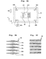
Fig. 3A shows a plan view illustrating an evaluation
mark plate 33 shown in Fig. 2, Fig. 3B shows a magnified
plan view illustrating an evaluating mark 48, and Fig. 3C
shows a magnified plan view illustrating an evaluating mark
49.
Fig. 4A shows a plan view illustrating a shot array on
a wafer for evaluating a resist coater and a developing
apparatus, Fig. 4B shows a magnified sectional view to
explain a method for measuring a resist pattern 49P, and
Fig. 4C shows a magnified sectional view illustrating
another example of a method for measuring the film
thickness of photoresist.
Figs. 5A and 5B illustrate a method for measuring a
resist pattern with wedge-shaped both ends.
Fig. 6A shows a plan view illustrating a shot array on
a wafer for evaluating a projection optical system of a
projection exposure apparatus, and Fig. 6B shows a
magnified plan view illustrating a resist pattern formed on
respective shot areas on the wafer.
Fig. 7A shows a plan view illustrating a shot array on
a wafer for evaluating the dynamic control characteristic
of the projection exposure apparatus, and Fig. 7B shows a
plan view illustrating a test reticle to be used for this
procedure.
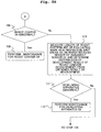
Figs. 8A and 8B show a flow chart illustrating the
former half of an evaluation sequence for the lithography
system according to an embodiment of the present invention.
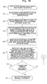
Figs. 9A and 9B show a flow chart illustrating the
latter half of the evaluation sequence for the lithography
system.
DESCRIPTION OF THE PREFERRED EMBODIMENTS
An exemplary embodiment of the present invention will
be explained below with reference to the drawings. In this
embodiment, the present invention is applied to a case in
which evaluation is made for various characteristics of a
lithography system for producing a semiconductor device,
comprising a resist coater, a projection exposure apparatus
as an exposure apparatus, and a developing apparatus
(developer).
Fig. 1 shows a schematic arrangement illustrating a
lithography system of this embodiment. With reference to
Fig. 1, a coater-developer section 51, which serves as a
substrate-processing apparatus, is installed to be in
contact with a chamber for surrounding a projection
exposure apparatus 50 in accordance with the in-line
system. A host computer 27 is installed to collectively
manage and control the entire operation of the projection
exposure apparatus 50 and the coater-developer section 51.
A transport line 52 for transporting a wafer as a substrate
is installed to traverse a central portion of the coater-developer
section 51. A first wafer cassette 53 for
accommodating a large number of unexposed wafers, and a
second wafer cassette 60 for accommodating a large number
of exposed and developed wafers are arranged at the first
end of the transport line 52. The second end of the
transport line 52 is installed just before a shutter-equipped
transport port (not shown) disposed at a side
surface of the chamber for the projection exposure
apparatus 50.
A resist coater 54 for applying a photoresist as a
photosensitive material onto the wafer, a pre-bake
apparatus 55 composed of a hot plate or the like for prebaking
the photoresist on the wafer, and a cooling
apparatus 56 for cooling the pre-baked wafer are installed
in a direction from the first wafer cassette 53 to the
projection exposure apparatus 50 along the first side
surface of the transport line 52 in the coater-developer
section 51. Those usable as the cooling apparatus 56
include, for example, an apparatus in which a pipe for
allowing cooling water to flow therethrough and a
temperature sensor are installed at the inside of a base
member for placing the wafer thereon, and an apparatus in
which a heat-absorbing element such as a Peltier element is
embedded in the base member. Further, a post-bake
apparatus 57 for baking the photoresist on the wafer after
the exposure, i.e., for performing so-called PEB (Post-Exposure
Bake), a cooling apparatus 58 for cooling the
wafer having been subjected to PEB, and a developing
apparatus 59 for developing the photoresist on the wafer
are installed in a direction from the projection exposure
apparatus 50 to the second wafer cassette 60 along the
second side surface of the transport line 52.
In the projection exposure apparatus 50 of this
embodiment, the wafer W as the exposure objective is held
on a wafer stage 39 by the aid of a wafer holder 38. The
wafer stage 39 is moved two-dimensionally on a wafer base
40 (see Fig. 2). A first guide member 42 is arranged to
extend substantially along an extension line of the central
axis of the transport line 52. A slider 43 is arranged so
that it is driven by an unillustrated linear motor along
the first guide member 42. A first arm 44 for holding the
wafer is installed rotatably and vertically movably on the
slider 43. A second guide member 46 is arranged
perpendicularly over the end of the first guide member 42.
A second arm 47 for holding the wafer is arranged so that
it is driven by an unillustrated linear motor along the
second guide member 46. The second guide member 46 extends
up to a wafer-loading position for the wafer stage 39. The
second arm 47 is also provided with a mechanism for making
sliding in a direction perpendicular to the second guide
member 46.
A delivery pin 45, which is capable of making rotation
and vertical movement for performing the prealignment for
the wafer, is installed in the vicinity of a position of
intersection between the guide members 42, 46. A position-detecting
unit (not shown) for detecting the positions of
two edge sections and a cutout (notch) disposed at the
outer circumference of the wafer is installed around the
delivery pin 45. A wafer loader system is constructed, for
example, by the guide members 42, 46, the slider 43, the
arms 44, 47, and the delivery pin 45.
Explanation will be made for an exemplary basic
operation of the lithography system shown in Fig. 1 in the
ordinary lithography step. One sheet of wafer, which is
taken out from the first wafer cassette 53 on the basis of
a command of the host computer 27, is transported to the
resist coater 54 via the transport line 52, and the
photoresist is applied to the wafer. The wafer, to which
the photoresist has been applied, is successively treated
by the pre-bake apparatus 55 and the cooling apparatus 56
along the transport line 52, and it is delivered to the
first arm 44 of the projection exposure apparatus. After
that, when the slider 43 arrives at the position in the
vicinity of the delivery pin 45 along the first guide
member 42, then the first arm 44 is rotated, and the wafer,
to which the photoresist is applied, is delivered from the
first arm 44 to the position A on the delivery pin 45. At
this position, the adjustment (prealignment) is performed
for the angle of rotation and the central position on the
basis of the contour of the wafer. After that, the wafer
is delivered to the second arm 47, and it is delivered to
the loading position for the wafer along the second guide
member 46. At this position, the wafer is loaded onto the
wafer holder 38 on the wafer stage 39. Exposure is
performed for respective shot areas on the wafer (referred
to as "wafer W") with the exposure light beam passing
through a predetermined device pattern on a reticle as a
mask.
The wafer W, for which the exposure has been
completed, is transported along the guide members 46, 42 up
to the transport line 52 of the coater-developer section
51. After that, the wafer W successively passes through
the post-bake apparatus 57 and the cooling apparatus 58
along the transport line 52, and it is fed to the
developing apparatus 59. A resist pattern, which resides
in a concave/convex structure corresponding to the device
pattern on the reticle, is formed on the respective shot
areas on the wafer W having been subjected to the
development in the developing apparatus 59. The wafer W,
for which the development has been performed as described
above, is transported along the transport line 52, and it
is accommodated in the second wafer cassette 60. After the
completion of the lithography step, for example, one lot of
wafers, which are accommodated in the second wafer cassette
60, are transported to a production line for executing, for
example, the pattern-forming step such as etching and ion
implantation and the resist-peeling off step.
In order to form, on the wafer W, a circuit pattern
which conforms to the designed data within an allowable
range, it is necessary that the resist pattern is formed on
the respective shot areas on the wafer W with a high degree
of resolution and a high degree of transfer faithfulness
respectively by using the lithography system shown in Fig.
1. For this purpose, at first, it is necessary to apply
the photoresist onto the entire surface of the wafer by
using the resist coater 54 as uniformly as possible to give
a target thickness. Secondly, it is necessary to perform
the exposure onto the wafer through the pattern on the
reticle by using the exposure apparatus 50 with a target
amount of exposure at a resolution as high as possible so
that the strain (distortion and magnification error) is
decreased as less as possible and the overlay accuracy is
increased as high as possible during the overlay exposure.
Finally, it is necessary to develop the photoresist on the
entire surface of the wafer under the target condition as
uniformly as possible by using the developing apparatus 59.
That is, it is necessary to perform the exposure in which
the characteristic of the resist coater 54 (uneven
application in this embodiment), the characteristic of the
projection exposure apparatus 50 (image formation
characteristic and overlay accuracy in this embodiment),
and the characteristic of the developing apparatus 59
(uneven development in this embodiment) are included in
predetermined allowable ranges respectively. For this
purpose, the projection exposure apparatus 50 of this
embodiment is incorporated with the mechanism for
evaluating any one of the predetermined characteristics of
the resist coater 54, the projection exposure apparatus 50
itself, and the developing apparatus 59, independently from
the characteristics of the other apparatuses respectively.
Fig. 2 shows a schematic arrangement of the projection
exposure apparatus 50 based on the step-and-scan manner of
this embodiment. With reference to Fig. 2, an ArF excimer
laser light source (wavelength: 193 nm) is used for an
exposure light source 1. However, those usable as the
exposure light source 1 include, for example, a KrF excimer
laser (wavelength: 248 nm), an F2 laser (wavelength: 157
nm), a Kr2 laser (wavelength: 146 nm), a high harmonic wave
generator such as a YAG laser, a high harmonic wave
generator such as a semiconductor laser, and a mercury
lamp. The exposure light beam IL (exposure beam) from the
exposure light source 1, which is composed of an
ultraviolet pulse light beam having a wavelength of 193 nm,
passes through a beam-matching unit (BMU) 2, and it comes
into a variable light-reducing unit 3 as a light
attenuator. An exposure control unit 21, which is provided
to control the amount of exposure with respect to the
photoresist on the wafer, controls the start, the stop, and
the output (oscillation frequency and pulse energy) of the
light emission of the exposure light source 1, and it
adjusts the dimming ratio at the variable light-reducing
unit 3 continuously or in a stepwise manner.
The exposure light beam IL, which has passed through
the variable light-reducing unit 3, passes through a beam-shaping
system 5 composed of lens systems 4A, 4B, and it
comes into a first fly's eye lens 6 which serves as a first
stage optical integrator (uniformizer or homogenizer). The
exposure light beam IL, which outgoes from the first fly's
eye lens 6, passes along a first lens system 7A, an optical
path-bending mirror 8, and a second lens system 7B, and it
comes into a second fly's eye lens 9 which serves as a
second stage optical integrator.
An aperture diaphragm plate 10 is arranged rotatably
by the aid of a driving motor 10e at a light-outgoing plane
of the second fly's eye lens 9, i.e., an optical Fourier
transformation plane (pupil plane of the illumination
system) with respect to the pattern plane (reticle plane)
of the reticle R as the exposure objective. The aperture
diaphragm plate 10 is switchably arranged with, for
example, a circular aperture diaphragm 10a for ordinary
illumination, an aperture diaphragm 10b for zonal
illumination, an aperture diaphragm for modified
illumination (not shown) composed of a plurality of (for
example, four) eccentric small apertures, and a small
circular aperture diaphragm (not shown) for a small
coherence factor (σ value). The main control system 22,
which collectively manages and controls the entire
operation of the projection exposure apparatus 50, rotates
the aperture diaphragm plate 10 by the aid of the driving
motor 10e to set the illumination condition.
In Fig. 2, the exposure light beam IL, which outgoes
from the second fly's eye lens 9 and which passes through
the aperture diaphragm 10a for the ordinary illumination,
comes into a beam splitter 11 which has a high
transmittance and a low reflectance. The exposure light
beam, which is reflected by the beam splitter 11, passes
through a light-collecting lens 19, and it comes into an
integrator sensor 20 composed of a photoelectric detector.
A detection signal of the integrator sensor 20 is supplied
to the exposure control unit 21. The relationship between
the detection signal of the integrator sensor 20 and the
illuminance of the exposure light beam IL on the wafer W as
the substrate to be exposed is previously measured highly
accurately, and it is stored in a memory in the exposure
control unit 21. The exposure control unit 21 is
constructed so that the illuminance (average value) of the
exposure light beam IL on the wafer W and the integral
value thereof can be indirectly monitored in accordance
with the detection signal of the integrator sensor 20.
The exposure light beam IL, which has been transmitted
through the beam splitter 11, passes through lens systems
12, 13 along the optical axis IAX, and it successively
comes into a fixed blind (fixed illumination field
diaphragm) 14A and a movable blind (movable illumination
field diaphragm) 14B. The latter movable blind 14B is
installed at a conjugate plane with respect to the reticle
plane. The former fixed blind 14A is arranged at a plane
which is defocused from the conjugate plane by a
predetermined amount. For example, as disclosed in
Japanese Patent Application Laid-Open No. 4-196513 and
United States Patent No. 5,473,410 corresponding thereto,
the fixed blind 14A has an opening which is arranged to
extend in a linear slit-shaped configuration or a
rectangular configuration (hereinafter collectively
referred to as "slit-shaped configuration") in a direction
perpendicular to the scanning exposure direction at the
center of the circular field of the projection optical
system PL. Further, the movable blind 14B, which
corresponds to the movable field diaphragm of the present
invention, is used to vary the width of the illumination
field area in the scanning direction in order to avoid any
unnecessary exposure upon the start and the end of the
scanning exposure for the respective shot areas on the
wafer W. Further, the movable blind 14B is also used to
vary the size of the pattern area of the reticle R or the
width thereof depending on the evaluation objective as
described later on in relation to the direction (non-scanning
direction) perpendicular to the scanning
direction. The information on the opening ratio of the
movable blind 14B is also supplied to the exposure control
unit 21. The value, which is obtained by multiplying the
illuminance determined from the detection signal of the
integrator sensor 20 by the opening ratio, represents the
actual illuminance on the wafer W.
The exposure light beam IL, which has passed through
the fixed blind 14A during the ordinary exposure, passes
along an optical path-bending mirror 15, a lens system 16
for image formation, a subsidiary condenser lens system 17,
and a main condenser lens system 18, and it illuminates an
illumination area (illumination field area) 35 of the
pattern plane (lower surface) of the reticle R as the mask.
Under the illumination light beam IL, the image of the
circuit pattern in the illumination area on the reticle R
is transferred at a predetermined projection magnification
β (β is, for example, 1/4 or 1/5) through the projection
optical system PL which is telecentric on both sides, to
the slit-shaped exposure area (projection area for a
pattern image conjugate with the illumination area 35) 35P
of the photoresist layer on the wafer W as the substrate
(substrate to be exposed) arranged on the image formation
plane of the projection optical system PL. The reticle R
and the wafer W can be regarded to be the first object and
the second object respectively. The wafer W is, for
example, a disk-shaped substrate of semiconductor (silicon
or the like) or SOI (silicon on insulator). The following
explanation will be made assuming that the Z axis extends
in parallel to the optical axis AX of the projection
optical system PL, the Y axis extends in the scanning
direction (direction parallel to the plane of paper of Fig.
2 in this embodiment) in the plane perpendicular to the Z
axis, and the X axis extends in the non-scanning direction
(direction perpendicular to the plane of paper of Fig. 2 in
this embodiment) perpendicular to the scanning direction.
With reference to Fig. 2, the reticle R is attracted
and held on a reticle stage 31. The reticle stage 31 is
placed on a reticle base 32 movably at a constant velocity
in the Y direction and finely movably in the X direction,
the Y direction, and the direction of rotation. The two-dimensional
position and the angle of rotation of the
reticle stage 31 (reticle R) are measured in real time by a
laser interferometer installed in a driving control unit
34. A driving motor (for example, a linear motor or a
voice coil motor) installed in the driving control unit 34
controls the scanning velocity and the position of the
reticle stage 31 on the basis of an obtained result of the
measurement and the control information supplied from the
main control system 22. The driving control unit 34 sets
the size of the opening of the movable blind 14B, or it
opens or closes the opening in the scanning direction on
the basis of the control information supplied from the main
control system 22. An evaluation mark plate 33, which is
composed of a glass substrate, is fixed in the vicinity of
the reticle R on the reticle stage 31.
Fig. 3A shows a plan view illustrating a state in
which the center of the evaluation mark plate 33 shown in
Fig. 2 is allowed to approximately coincide with the
optical axis AX. With reference to Fig. 3A, when the
characteristic of the projection exposure apparatus 50 is
evaluated, the illumination area 35 for the exposure light
beam is set as indicated by two-dot chain lines so that the
approximate entire evaluation mark plate 33 is covered
therewith. The illumination area 35 is set to
approximately inscribe the circular effective field of the
projection optical system PL shown in Fig. 2, and it is a
rectangular area which is slender in the non-scanning
direction (X direction) perpendicular to the scanning
direction SD (Y direction). For example, four identical
two-dimensional evaluating marks 36A, 36B,... 36D are
formed at positions close to the four apexes of the
illumination area 35 on the evaluation mark plate 33 so
that they are included at the inside of the illumination
area 35. The evaluating mark 36A is a two-dimensional mark
constructed by combining an X axis mark 37X which is
composed of a line-and-space pattern arranged at a
predetermined pitch in the X direction, and a Y axis mark
37Y which is composed of a line-and-space pattern arranged
at a predetermined pitch in the Y direction. The line
width of the line-and-space pattern for constructing the
evaluating mark 36A is, for example, a line width which is
approximately in a range of 1x (equal) to 2x (two times)
with respect to the limit resolution of the projection
optical system PL shown in Fig. 2. In this case, for
example, each of the evaluating marks may be constructed
with a plurality of line-and-space patterns having
different line widths (for example, pitches or duties).
On the other hand, when the characteristic of the
resist coater 54 or the developing apparatus 59 shown in
Fig. 1 is evaluated, the illumination area 35A is set as
indicated by dashed lines in a narrow area about the center
of the optical axis AX at the central portion of the
evaluation mark plate 33 shown in Fig. 3 by narrowing the
opening of the movable blind 14B shown in Fig. 2. The
illumination area 35A is, for example, an area in which the
widths in the X direction and the Y direction are about 1/5
with respect to the illumination area 35 respectively. Two
evaluating marks 48, 49 are formed adjacently on the
evaluation mark plate 33 at the central portion of the
illumination area 35A. The illumination area 35A is the
narrow area disposed about the center of the optical axis
AX in the field of the projection optical system PL.
Therefore, the image of the pattern in the illumination
area 35A is projected onto the image plane side by the aid
of the projection optical system PL in a state in which any
aberration is scarcely generated.
In this embodiment, as shown in a magnified view in
Fig. 3B, the first evaluating mark 48 is formed such that a
plurality of marks 48a to 48e, each of which has a rhombus-shaped
configuration slender in the measuring direction (X
direction in this embodiment), i.e., each of which has
wedge-shaped configurations at both ends in the measuring
direction, are arranged at a predetermined pitch in the
direction (Y direction) perpendicular to the measuring
direction. The thickest portion of the mark 48a to 48e has
a line width which is approximately in a range of 1x
(equal) to 2x (two times) with respect to the limit
resolution of the projection optical system PL shown in
Fig. 2. The evaluating mark 48 is used to evaluate the
characteristic of the developing apparatus 59 shown in Fig.
1. As shown in a magnified view in Fig. 3C, the second
evaluating mark 49 resides in a line-and-space pattern
arranged at a predetermined pitch in the Y direction. The
line width of each of marks of the evaluating mark 49 is a
loose (coarse) line width which is about several times the
limit resolution of the projection optical system PL. The
evaluating mark 49 is used to evaluate the characteristic
of the resist coater 54 shown in Fig. 1.
Returning to Fig. 2, the wafer W is attracted and held
on the wafer stage 39 by the aid of the wafer holder 38.
The wafer stage 39 is movable two-dimensionally along the
XY plane parallel to the image plane of the projection
optical system PL on the wafer base 40. That is, the wafer
stage 39 is movable at a constant velocity in the Y
direction on the wafer base 40, and it is movable in a
stepping manner in the X direction and the Y direction.
The wafer stage 39 is further incorporated with a Z
leveling mechanism for controlling the position of the
wafer W in the Z direction (focus position) and the angles
of rotation about the X axis and the Y axis as well. A
multi-point autofocus sensors 25A, 25B, which are composed
of a projecting optical system 25A for obliquely projecting
a slit image onto a plurality of measuring points on the
surface (detection surface) on the wafer W, and a light-receiving
optical system 25B for receiving the reflected
light beam from the detection surface to generate focus
signals corresponding to the focus positions of the
plurality of measuring points, are also provided at the
side surface of the projection optical system PL. The
focus signals thereof are supplied to a focusing control
unit in the main control system 22.
During the scanning exposure, the focusing control
unit in the main control system 22 continuously drives the
Z leveling mechanism in the wafer stage 39 in accordance
with the autofocus system on the basis of the information
of the focus signals (focus positions). Accordingly, the
surface of the wafer W is focused to the image plane of the
projection optical system PL. When the characteristic is
evaluated, for example, the Z leveling mechanism is driven
on the basis of the focus signals. Accordingly, the focus
position of the wafer W can be controlled in an arbitrary
amount.
The positions of the wafer stage 39 in the X direction
and the Y direction, and the angles of rotation about the X
axis, the Y axis, and the Z axis are measured in real time
by the laser interferometer in the driving control unit 41.
The driving motor (for example, a linear motor) in the
driving control unit 41 controls the scanning velocity and
the position of the wafer stage 39 on the basis of the
obtained result of the measurement and the control
information supplied from the main control system 22.
When the scanning exposure is performed, it is
necessary to previously perform the alignment for the
reticle R and the wafer W. Therefore, a reticle alignment
microscope (not shown) for measuring the position of the
alignment mark (reticle mark) on the reticle R is installed
on the reticle stage 31. Further, in order to measure the
position of the alignment mark (wafer mark) on the wafer W,
a first alignment sensor 23, which is based on the off-axis
system and which is based on the image processing system
(FIA system: Field Image Alignment system), is installed at
the side surface of the projection optical system PL. The
alignment sensor 23 is operated as follows. That is, for
example, the detection mark is irradiated with an
illumination light beam having a relatively wide wavelength
region from a halogen lamp or the like. The image of the
detection mark is photographed together with the index
mark. An obtained image signal is processed to determine
the positional discrepancy amounts of the detection mark in
the X direction and the Y direction with respect to the
index mark. Further, the line widths of individual marks
for constructing the detection mark are determined.
Obtained measured values are supplied to the main control
system 22.
In order to measure the position of the wafer mark in
accordance with another system as well, a second alignment
sensor 24, which is based on the off-axis system, is
provided on the side surface of the projection optical
system PL. The alignment sensors 23, 24 correspond to the
second sensor and the first sensor of the present invention
respectively. The alignment sensor 24 comprises a sensor
24a (hereinafter referred to as "LIA sensor 24a") based on
the LIA (Laser Interferometric Alignment) system for
radiating two light fluxes (or one light flux in some
cases) having slightly different frequencies onto the
diffraction grating-shaped detection mark and detecting the
interference light composed of a plurality of interference
light beams generated from the detection mark, and a sensor
24b (hereinafter referred to as "LSA sensor 24b") for
relatively scanning the dot array-shaped detection mark and
the laser beam radiated in a slit-shaped configuration and
detecting the diffracted light generated from the detection
mark. As for the LIA sensor 24a, for example, the more
detailed arrangement is disclosed in Japanese Patent
Application Laid-Open No. 2-227602 (Japanese Patent No.
2814520 and United States Patent No. 5,489,986
corresponding thereto). As for the LSA sensor 24b, for
example, the more detailed arrangement is disclosed in
Japanese Patent Application Laid-Open No. 60-130742
(Japanese Patent Publication No. 6-16478 and United States
Patent No. 4,677,301 corresponding thereto). In this
embodiment, in place of the LIA sensor 24a, a sensor may be
adopted, which is based on a system in which one coherent
beam is radiated substantially perpendicularly onto a
detection mark to cause interference and receive at least a
pair of diffracted light beams (for example, ±n-order
diffracted light beams having an equal order) generated
from the detection mark.
A photoelectrically converted signal (detection
signal) of the interference light of the LIA sensor 24a and
a photoelectrically converted signal (detection signal) of
the diffracted light of the LSA sensor 24b are supplied to
an alignment signal-processing unit in the main control
system 22 respectively. The alignment signal-processing
unit detects the coordinate of the detection mark during
the alignment by using the detection signal of the LIA
sensor 24a or the LSA sensor 24b and the measured value of
the coordinate of the wafer stage 39. When the
characteristic of the lithography system is evaluated, the
alignment signal-processing unit calculates the thickness
of the resist pattern on the detection mark from the
magnitude of the detection signal of the LIA sensor 24a,
and it calculates the length of the detection mark in the
measuring direction by using the detection signal of the
LSA sensor 24b and the coordinate of the wafer stage 39.
The scanning exposure is performed after performing
the alignment for the wafer W by using the alignment sensor
23 or 24. That is, the main control system 22 sends
various pieces of information including, for example, the
movement positions, the movement velocities, the rates of
acceleration of movement, and the position offsets of the
reticle stage 31 and the wafer stage 39 respectively, to
the driving control units 34, 41. In response thereto, the
reticle R is scanned at the velocity Vr in the +Y direction
(or in the -Y direction) with respect to the illumination
area 35 of the exposure light beam IL by the aid of the
reticle stage 31, in synchronization with which the wafer W
is scanned at the velocity β·Vr (β represents the
projection magnification from the reticle R to the wafer W)
in the -Y direction (or in the +Y direction) with respect
to the exposure area 35P for the pattern image on the
reticle R by the aid of the wafer stage 39. In order to
avoid any exposure onto unnecessary portions at the start
and the end of the scanning exposure during this process,
the opening/closing operation of the movable blind 14B is
controlled by the driving control unit 34. The reason why
the movement direction of the reticle R is opposite to that
of the wafer W is that the projection optical system PL of
this embodiment performs the inverting projection.
Further, the main control system 22 reads, from the
exposure data file, various exposure conditions for
performing the scanning exposure in a proper exposure
amount for the photoresist in each of the shot areas on the
wafer W, and it executes the optimum exposure sequence in
cooperation with the exposure control unit 21 as well.
That is, when the command to start the scanning exposure
for one shot area on the wafer W is issued from the main
control system 22 to the exposure control unit 21, then the
exposure control unit 21 starts the light emission of the
exposure light source 1, and it calculates the integral
value of the illuminance of the exposure light beam IL for
the wafer W (sum of the pulse energy per unit time) by the
aid of the integrator sensor 20. The integral value is
reset to zero upon the start of the scanning exposure. The
exposure control unit 21 successively calculates the
integral value of the illuminance, and it controls the
output of the exposure light source 1 (oscillation
frequency and pulse energy) and the dimming ratio of the
variable light-reducing unit 3 depending on an obtained
result so that the proper exposure amount is obtained at
respective points on the photoresist on the wafer W after
the scanning exposure. The light emission of the exposure
light source 1 is stopped after completion of the scanning
exposure for the concerning shot area.
Next, explanation will be made with reference to a
flow chart shown in Figs. 8A and 8B and Figs.9A and 9B for
an example of the operation (evaluation sequence) for
evaluating the predetermined characteristics of the resist
coater 54, the projection exposure apparatus 50, and the
developing apparatus 59 of the lithography system shown in
Fig. 1 of this embodiment. The evaluation of the
characteristics may be executed periodically.
Alternatively, for example, the evaluation may be executed
when the type of the photoresist is changed, or when the
development process is changed.
At first, in the step 101 shown in Fig. 8, the
photoresist is applied to an unexposed wafer W1 by using
the resist coater 54 shown in Fig. 1 under the control of
the host computer 27. After that, the wafer W1 is treated
with the pre-bake apparatus 55 and the cooling apparatus
56, and it is loaded onto the wafer stage 39 (wafer holder
38) of the projection exposure apparatus 50 (step 102).
Subsequently, the reticle stage 31 shown in Fig. 2 is
driven to allow the center of the evaluation mark plate 33
to coincide with the center of the effective field (optical
axis AX) of the projection optical system PL (step 103).
The movable blind 14B is controlled to set the illumination
area of the exposure light beam IL to the central narrow
illumination area 35A of the effective field as shown in
Fig. 3A (step 104). In this state, only the evaluating
marks 48, 49 can be illuminated. Images of the evaluating
marks 48, 49 can be projected in a state in which there is
little influence of the aberration of the projection
optical system PL.
In the step 105, the projection exposure apparatus 50
shown in Fig. 2 is regarded to be a projection exposure
apparatus of the full field exposure type, and the
respective shot areas SA on the wafer W1 are exposed with
the images of the evaluating marks 48, 49 in the
illumination area 35A by the aid of the projection optical
system PL in accordance with the step-and-repeat manner.
Fig. 4A shows the wafer W1 exposed as described above.
With reference to Fig. 4A, the exposure surface of the
wafer W1 is divided into N1 individuals of shot areas SA1,
SA2,... SAN1 (they are representatively referred to as "shot
areas SA") each having approximately the same size as that
of the conjugate image of the illumination area 35A which
is narrow in the X direction and the Y direction. The
respective shot areas SA are exposed with the images 48P,
49P of the evaluating marks 48, 49 respectively. In the
next step 106, the wafer W1 after the exposure is
transported to the developing apparatus 59 via the post-bake
apparatus 57 and the cooling apparatus 58 shown in
Fig. 1. In the developing apparatus 59, the photoresist on
the wafer W1 is developed. The wafer W1 after the
development is transported via the transport line 52, and
it is loaded onto the wafer stage 39 of the projection
exposure apparatus 50 again. In this case, resist patterns
(also referred to as 48P, 49P), which have a concave/convex
structure corresponding to the images 48P, 49P of the
evaluating marks 48, 49 respectively, are formed on the
respective shot areas SA on the wafer W1 shown in Fig. 4A.
As shown in Fig. 4B, the latter resist pattern 49P is a
diffraction grating-shaped mark having a predetermined
pitch in the X direction. As shown in Fig. 5A, the former
resist pattern 48P is a plurality of concave/convex
patterns with both sides having wedge-shaped
configurations.
In the subsequent step 107, detection signals, which
correspond to the intensities of the interference light
beams (diffracted light beams) from the resist patterns 49P
of all of the shot areas SA on the wafer W1 shown in Fig.
4A, are detected by using the LIA sensor 24a of the
alignment sensor 24 under the control of the main control
system 22 shown in Fig. 2. Results of the detection are
supplied to the host computer 27. As shown in Fig. 4B, two
light fluxes LA, LB are radiated from the LIA sensor 24a
onto the resist pattern 49P. The +1-order diffracted light
LA1 of the light flux LA and the -1-order diffracted light
LB1 of the light flux LB are generated in parallel as
interference light from the resist pattern 49P, and the
interference light is detected. In this case, the average
value of the intensities of the interference light varies
depending on the film thickness of the remaining resist,
i.e., the difference in height of the resist pattern 49P on
each of the shot areas SA. Therefore, for example, the
relationship between the difference in height of the resist
pattern 49P and the average value of the detection signals
of the interference light is previously determined
experimentally to obtain a table which is stored in the
data file of the host computer 27 beforehand. The host
computer 27 determines the distribution of the film
thickness of the resist remaining on the wafer W1 from the
table and the average value of the detection signals of the
interference light in the respective shot areas SA. The
host computer 27 estimates, as the uneven application, the
dispersion of the film thickness (for example, standard
deviation) and the average film thickness obtained when the
photoresist is applied to the wafer W1 with the resist
coater 54, from the film thickness distribution.
In the next step 108, the host computer 27 checks
whether or not the resist coater 54 is abnormal, i.e.,
whether or not the average film thickness of the
photoresist and the dispersion of the film thickness
estimated in the step 107 are included within allowable
ranges with respect to the target values (0 for the
dispersion) prescribed for the photoresist of the
concerning type. If there is any abnormality, the host
computer 27 issues alarm information on the resist coater
54 to the operator. In response thereto, the maintenance
is performed for the resist coater 54 in the step 109.
After that, the evaluation sequence of the steps 101 to 108
may be executed again for another unexposed wafer W2.
In the embodiment described above, the resist pattern
49P which has been developed is detected in order to
evaluate the resist coater 54. However, as shown in Fig.
4C, the following procedure may be available. That is, a
concave/convex diffraction grating-shaped mark 61 is formed
on each of the shot areas SA on the wafer W1 beforehand.
After the photoresist PH is applied onto the wafer W1, the
light fluxes LA, LB are radiated onto the mark 61 from the
LIA sensor 24a to detect the interference light (LA1, LB1)
from the mark 61. Also in this case, the average value of
intensities of the interference light from the mark 61
varies depending on the film thickness of the photoresist
PH on the shot area SA. Therefore, the film thickness
distribution of the photoresist PH on the wafer W1 can be
determined from detection signals of the LIA sensor 24a
without performing the exposure and the development. In
this example, the resist coater 54 can be evaluated for a
short period of time, because the exposure step and the
development step can be omitted. A light beam having a
wavelength, which is not absorbed by the photoresist PH,
i.e., with which the photoresist PH is not exposed, is used
as the light fluxes LA, LB from the LIA sensor 24a.
In place of the detection of the resist pattern 49P
which has been developed, a latent image of the evaluating
mark 49 formed on the resist may be detected, for example,
by using the LIA sensor 24a. The average film thickness of
the photoresist and the film thickness distribution may be
determined on the basis of the obtained detection result.
In this case, the resist coater 54 can be evaluated for a
short period of time, because the development step for the
photoresist can be omitted. A light beam having a
wavelength, which is not absorbed by the photoresist PH,
i.e., with which the photoresist PH is not exposed, is used
as the light fluxes LA, LB from the LIA sensor 24a.
Similarly, the projection exposure apparatus 50 shown
in Fig. 2 may be provided with a film thickness-measuring
unit based on the interferometer system or the ellipsometer
system. The thickness distribution of the photoresist on
the wafer may be directly measured with the film thickness-measuring
unit before the exposure. Further, for example,
the film thickness of the photoresist, the dispersion
thereof and other factors may be detected by using an
interatomic force microscope. When the uneven application
as described above is estimated by transferring the
evaluating mark 48, 49 onto the photoresist, a state is
regarded to be established in this embodiment, in which
there is little influence of the aberration of the
projection optical system PL, by arranging the evaluating
mark 48, 49 at the center (on the optical axis AX) of the
projection field of the projection optical system PL.
However, when it is impossible to neglect the influence of
the aberration of the projection optical system PL, the
following procedure is preferably adopted. That is, the
information on aberration (for example, wave front
aberration) of the projection optical system PL is
previously determined by means of a method which does not
undergo the influence of the uneven application or the
like, for example, by means of the spatial image
measurement in which a projected image of an evaluating
mark is detected on the image plane side of the projection
optical system PL. The uneven application or the like is
determined based on the use of the information on
aberration as well.
The maintenance operation for the resist coater 54 in
the step 109 also includes, for example, the resetting
operation (change) for the application condition for the
photoresist (including, for example, the rotation speed and
the number of revolution of the wafer in the case of the
spin coat method, or including, for example, the movement
speeds of the wafer and the nozzle in the case of the scan
coat system). Further, an operator may adjust the resist
coater 54, for example, on the basis of the film thickness
and the dispersion thereof determined in the step 107.
Alternatively, the host computer 27 may give a command to
the resist coater 54 to perform, for example, the change of
the application condition.
If the resist coater 54 is not abnormal, the operation
proceeds from the step 108 to the step 110. In this
procedure, the detection signals, which correspond to the
diffracted light from the resist patterns 48P of all of the
shot areas SA on the wafer W1 shown in Fig. 4A, are
incorporated by the main control system 22 shown in Fig. 2
while corresponding to the X coordinates of the wafer stage
39 by using the LSA sensor 24B of the alignment sensor 24.
The laser beam LS is radiated in a slit-shaped
configuration from the LSA sensor 24b so that the laser
beam LS extends in the Y direction as depicted with the
shot area SAi shown in Fig. 5A. When the wafer stage 39 is
driven in the X direction to relatively scan the resist
pattern 48P and the laser beam LS, the diffracted light is
generated from the resist pattern 48P provided that even a
part of the resist pattern 48P is irradiated with the laser
beam LS. Accordingly, the main control system 22
determines a range of the X coordinate of the wafer stage
39 at which the level of the detection signal of the
diffracted light is not less than a predetermined value.
This range is regarded to be the length LX1 of the resist
pattern 48P in the shot area SAi. Similarly, the main
control system 22 determines the lengths of the resist
pattern 48P in all of the shot areas SA. Measured values
are supplied to the host computer 27.
In this case, if it is assumed that the state of the
development is unsatisfactory, for example, in the shot
area SAj shown in Fig. 5B, the length LX2 of the resist
pattern 48P is smaller than LX1. Therefore, the length of
the resist pattern 48 corresponds to the state of the
development. On the basis of this principle, the host
computer 27 assumes that the average value of the lengths
of the resist patterns 48P in all of the shot areas SA on
the wafer W1 and the dispersion (for example, standard
deviation) represent the uneven development caused upon the
development for the photoresist in the developing apparatus
59.
In the next step 111, the host computer 27 checks
whether or not the developing apparatus 59 is abnormal,
i.e., whether or not the uneven development (average value
of the length of the resist pattern 48P and the dispersion)
determined in the step 110 is included in an allowable
range with respect to the target value (0 for the
dispersion) prescribed for the photoresist of the
concerning type. If there is any abnormality, the host
computer 27 issues alarm information on the developing
apparatus 59 to the operator. In response thereto, the
maintenance is performed for the developing apparatus 59 in
the step 112. In the step 112, for example, the change of
the development condition (for example, the development
time) for the developing apparatus 59 based on the uneven
development is performed, for example, by the operator or
the host computer 27. After that, the evaluation sequence
corresponding to the steps 101 to 106, 110, 111 may be
executed again.
If the developing apparatus 59 is not abnormal as
well, the operation proceeds from the step 111 to the step
120 shown in Fig. 9A to evaluate the image formation
characteristics of the projection exposure apparatus 50.
For this purpose, the photoresist is applied to an
unexposed wafer (referred to as "W3") by using the resist
coater 54 shown in Fig. 1 under the control of the host
computer 27. After that, the wafer W3 is treated with the
pre-bake apparatus 55 and the cooling apparatus 56, and it
is loaded onto the wafer stage 39 of the projection
exposure apparatus 50 (step 121). Subsequently, the
opening of the movable blind 14B is opened in a state in
which the center of the evaluation mark plate 33 shown in
Fig. 2 is allowed to coincide with the optical axis AX so
that the illumination area of the exposure light beam IL is
set to be the illumination area 35 having the ordinary size
as shown in Fig. 3A (step 122). In this state, the
evaluating marks 36A to 36D, which are disposed at the
periphery of the effective field of the projection optical
system PL, can be illuminated.
In the step 123, the projection exposure apparatus 50
shown in Fig. 2 is regarded as a projection exposure
apparatus of the full field exposure type, and the
respective shot areas SB on the wafer W3 are exposed with
the images of the evaluating marks 36A to 36D in the
illumination area 35 by the aid of the projection optical
system PL in accordance with the step-and-repeat manner.
Fig. 6A shows the wafer W3 exposed as described above.
With reference to Fig. 6A, the exposure surface of the
wafer W3 is divided into N2 (N2 < N1) individuals of shot
areas SB1, SB2,... SBN2 (they are representatively referred
to as "shot areas SB") each having approximately the same
size as that of the conjugate image of the illumination
area 35 which is slender in the X direction and the Y
direction. The respective shot areas SB are exposed with
the images 36AP to 36DP of the evaluating marks 36A to 36D
respectively. In the next step 124, the wafer W3 after the
exposure is transported to the developing apparatus 59 via
the post-bake apparatus 57 and the cooling apparatus 58
shown in Fig. 1. In the developing apparatus 59, the
photoresist on the wafer W3 is developed. The wafer W3
after the development is transported via the transport line
52, and it is loaded onto the wafer stage 39 of the
projection exposure apparatus 50 again. In this case,
resist patterns (also referred to as 36AP to 36DP), which
have a concave/convex structure corresponding to the images
of the evaluating marks 36A to 36D respectively, are formed
in the respective shot areas SB on the wafer W3 shown in
Fig. 6A. Representatively, the resist pattern 36AP is
composed of line-and-space patterns 37XP, 37YP each having
a concave/convex structure arranged in the X direction and
the Y direction respectively as shown in Fig. 6B.
In the subsequent step 125, the line widths and the
positions (X coordinates, Y coordinates) of the resist
patterns 36AP to 36DP of all of the shot areas SB on the
wafer W3 shown in Fig. 6A are measured by using the
alignment sensor 23 based on the FIA system under the
control of the main control system 22 shown in Fig. 2.
Measured values are supplied to the host computer 27. For
example, in the case of the resist pattern 36AP shown in
Fig. 6B, the widths hX, hY of the ridges (resist portions)
of the line-and-space patterns 37XP, 37YP are measured. In
this case, the resist coater 54 and the developing
apparatus 59 have been adjusted so that the satisfactory
characteristics are obtained in this embodiment.
Therefore, the line width and the position of the resist
pattern 36AP to 36DP depend on the image formation
characteristic (for example, the resolution and the
aberration) of the projection optical system PL. However,
even in the case of the resist coater 54 and the developing
apparatus 59, the uneven application and the uneven
development remain to some extent. Therefore, the host
computer 27 averages the line widths and the positions of
the resist patterns 36AP to 36DP in all of the measured
shot areas SB to determine the line width and the position
of the resist pattern 36AP to 36DP on the image plane of
the projection optical system PL. The host computer 27
evaluates the resolution of the projection optical system
PL by comparing the line width with the designed value.
The host computer 27 evaluates the distortion (including
the magnification error) of the projection optical system
PL by comparing the positions of the four resist patterns
36AP to 36DP with the designed values.
In the next step 126, the host computer 27 checks
whether or not the projection optical system PL is
abnormal, i.e., whether or not the resolution and the
distortion evaluated in the step 125 are included in
allowable ranges with respect to the target values. If
there is any abnormality, the host computer 27 issues alarm
information on the projection optical system PL to the
operator. Corresponding thereto, the adjustment is
performed for the projection optical system PL in the step
127. In this case, although not shown, the projection
optical system PL shown in Fig. 2 is provided with an image
formation characteristic-adjusting mechanism which makes it
possible to finely move a plurality of predetermined lenses
in the optical axis direction respectively and incline the
plurality of predetermined lenses. The image formation
characteristic-adjusting mechanism is used to adjust the
projection optical system PL. After that, the evaluation
sequence corresponding to the steps 120 to 126 may be
executed again. Such an image formation characteristic-adjusting
mechanism is disclosed in Japanese Patent
Application Laid-Open No. 6-45217 and United States Patent
No. 6,078,380 corresponding thereto which are incorporated
herein by reference. The image formation characteristic-adjusting
mechanism of this embodiment can shift the
central wavelength of the exposure light beam IL generated
from the exposure light source 1 by controlling a
wavelength-adjusting section of the exposure light source
1. The image formation characteristic of the projection
optical system PL can be also adjusted by means of the
wavelength shift.
If the image formation characteristics of the
projection optical system PL are not abnormal, the
operation proceeds from the step 126 to the step 128 to
evaluate the final dynamic characteristic of the projection
exposure apparatus 50 in this procedure. For this purpose,
the photoresist is applied to an unexposed wafer (referred
to as "W4") by using the resist coater 54 shown in Fig. 1
under the control of the host computer 27. After that, the
wafer W4 is treated with the pre-bake apparatus 55 and the
cooling apparatus 56, and it is loaded on the wafer stage
39 of the projection exposure apparatus 50 (step 129).
Subsequently, a test reticle R1 shown in Fig. 7B is loaded
onto the reticle stage 31 shown in Fig. 2 (step 130). As
shown in Fig. 7B, three pairs of two-dimensional evaluating
marks 62A to 62C, 62D to 62F are formed at predetermined
intervals in the scanning direction SD (Y direction) in the
pattern area of the test reticle R1. Each of the
evaluating marks 62A to 62F is formed, for example, with
two line-and-space patterns in the same manner as the
evaluating mark 36A shown in Fig. 3A.
In the step 131, the respective shot areas SC on the
wafer W4 are exposed with the images of the evaluating
marks 62A to 62F on the test reticle R1 by the aid of the
projection optical system PL in accordance with the step-and-scan
manner (scanning exposure manner) by using the
projection exposure apparatus 50 shown in Fig. 2. In this
procedure, with reference to Fig. 7B, the test reticle R1
is scanned in the scanning direction SD with respect to the
illumination area 35. Corresponding thereto, as shown in
Fig. 7A, the respective shot areas on the wafer W4 is
scanned with respect to the slit-shaped exposure area 35P.
Fig. 7A shows the wafer W4 exposed as described above.
With reference to Fig. 7A, the exposure surface of the
wafer W4 is divided into N3 (N3 < N2) individuals of shot
areas SC1, SC2, ... SCN2 (they are representatively referred
to as "shot areas SC") each having approximately the same
size as that of the device to be produced, at predetermined
pitches in the X direction and the Y direction. The
respective shot areas SC are exposed with the images 62AP
to 62FP of the evaluating marks 62A to 62F respectively.
In the next step 132, the wafer W4 after the exposure is
transported to the developing apparatus 59 via the post-bake
apparatus 57 and the cooling apparatus 58 shown in
Fig. 1. In the developing apparatus 59, the photoresist on
the wafer W4 is developed. The wafer W4 after the
development is transported via the transport line 52, and
it is loaded onto the wafer stage 39 of the projection
exposure apparatus 50 again. In this case, resist patterns
(also referred to as 62AP to 62FP), which have a
concave/convex structure corresponding to the images of the
evaluating marks 62A to 62F respectively, are formed on the
respective shot areas SC on the wafer W4 shown in Fig. 7A.
In the subsequent step 133, the line widths and the
positions (X coordinates, Y coordinates) of the resist
patterns 62AP to 62FP of all of the shot areas SC on the
wafer W4 shown in Fig. 7A are measured by using the
alignment sensor 23 based on the FIA system under the
control of the main control system 22 shown in Fig. 2.
Measured values are supplied to the host computer 27. The
host computer 27 determines the average value and the
dispersion (for example, standard deviation) of the line
widths and the positions of the resist patterns 62AP to
62FP in all of the measured shot areas SC to compare the
measured values with the designed values. Thus, the host
computer 27 evaluates the dynamic control characteristic
(for example, synchronization characteristic between the
reticle stage and the wafer stage) during the scanning
exposure of the projection exposure apparatus 50. The
image formation characteristic such as the distortion of
the projection optical system PL may be detected as the
dynamic control characteristic in the same manner as
described above.
In the next step 134, the host computer 27 checks
whether or not the dynamic control characteristic is
abnormal. If there is any abnormality, the host computer
27 issues alarm information on the dynamic control
characteristic to the operator. Corresponding thereto, the
adjustment is performed in the step 135 for the stage
system including, for example, the reticle stage 31, the
wafer stage 39, and the laser interferometers for measuring
the positions of them. After that, the evaluation sequence
corresponding to the steps 128 to 134 may be executed
again. If there is no abnormality in the dynamic control
characteristic in the step 134, the operation proceeds to
the step 136 to execute the ordinary exposure step for the
device pattern.
For example, when the resolution and the image
formation characteristic of the projection optical system
PL are checked in the step 126 described above, latent
images of the evaluating marks 36A to 36D, which are formed
on the photoresist on the wafer, may be detected with the
alignment sensor 23 to obtain the line width and the
position information thereof without performing the
development treatment for the photoresist so that the
resolution and the image formation characteristic may be
determined on the basis of obtained results of the
measurement. In this case, the evaluation of the
resolution and the image formation characteristic is not
affected by the development treatment, because the
development treatment is not applied. Therefore, for
example, the resolution can be evaluated for a short period
of time without determining the uneven development, for
example, in the step 110. Also when the dynamic control
characteristic is evaluated in the step 133, the latent
images may be detected in place of the resist patterns of
the evaluating marks 62A to 62F in the same manner as
described above. As described above, it is unnecessary to
use the characteristic of the uneven development when the
evaluation is made for the resolution and the image
formation characteristic and when the evaluation is made
for the dynamic control characteristic. However, in order
to evaluate the developing apparatus 59 which is the part
of the coater-developer section 51 (substrate-processing
apparatus), it is necessary to obtain the characteristic of
the uneven development. Therefore, the uneven development
may be separately detected, if necessary.
In the embodiment described above, both of the uneven
application of the photoresist and the uneven development
are determined. However, when the latent image detection
is utilized as described above, only the uneven application
may be determined. Alternatively, in the case of a process
(layer) in which the influence of the uneven application is
considered to be small, only the uneven development may be
determined. In the embodiment described above, the image
formation characteristic of the projection exposure
apparatus 50 is determined. However, no problem arises
even when only at least one of the uneven application and
the uneven development is determined without determining
the image formation characteristic.
As described above, in the evaluation sequence for the
lithography system of this embodiment, the movable blind
14B is used as the variable field diaphragm to expose the
wafer for evaluation with the images of the evaluating
marks 48, 49 in the narrow field. Therefore, the
characteristic of the projection exposure apparatus 50 can
be distinguished from the characteristic of the resist
coater 54 or the developing apparatus 59 to perform the
evaluation with ease. Further, the two types of the
evaluating marks 48, 49 are used. Therefore, the
characteristic of the resist coater 54 can be distinguished
from the characteristic of the developing apparatus 59 to
perform the evaluation with ease. Accordingly, the
lithography system can be adjusted easily and quickly. In
the embodiment described above, when the uneven application
or the uneven development exceeds the allowable range,
namely when any abnormality is observed in the resist
coater 54 or the developing apparatus 59, then the
maintenance (for example, the change of the application
condition or the development condition) is performed for
the resist coater 54 or the developing apparatus 59 in the
steps 109, 111. However, the uneven application or the
uneven development cannot be included within the allowable
range in some cases even when the maintenance has been
performed. Therefore, for example, the exposure condition
(for example, the exposure amount) for the wafer, which is
determined by the projection exposure apparatus 50, may be
changed so that the change of the line width of the circuit
pattern or the like to be formed on the wafer, which would
be otherwise caused, for example, by the uneven application
or the uneven development, may be compensated. For
example, the exposure amount is allowed to partially differ
on the wafer depending on the uneven application or the
uneven development. Accordingly, even when the uneven
application or the uneven development cannot be included
within the allowable range, the line width, the shape, and
other features of the circuit pattern formed on the wafer
can be allowed to substantially coincide with the preset
data. Further, when the exposure condition as described
above is changed depending on the uneven application or the
uneven development, it is even allowable that the steps
109, 112 shown in Fig. 8 are not executed in the embodiment
described above. Further, even when the uneven application
or the uneven development is included within the allowable
range, for example, the change of the exposure condition as
described above may be performed, if necessary.
Further, in the embodiment described above, for
example, when any abnormality is observed in the resist
coater 54, then the photoresist may be applied to the wafer
again to transfer the evaluating mark after performing the
maintenance for the resist coater 54, and a transferred
image may be detected to determine the uneven development.
Alternatively, the detection result of the uneven
development in the step 110 may be corrected on the basis
of the uneven application. Further, when any abnormality
is observed in at least one of the resist coater 54 and the
developing apparatus 59, the measurement result of the
image formation characteristic of the projection exposure
apparatus 50 may be corrected on the basis of at least one
of the uneven application and the uneven development in the
same manner as described above. Alternatively, for
example, the evaluating mark may be transferred again after
performing the maintenance for at least one of the
apparatuses.
In the embodiment described above, when the image of
the evaluating mark is projected onto the photoresist in
order to detect the characteristic (uneven application or
uneven development) of the resist coater 54 or the
developing apparatus 59, the narrow field is obtained by
using the movable blind 14B. Therefore, the uneven
application or the uneven development can be evaluated at a
fine spacing distance on the exposure surface on the wafer.
However, if it is unnecessary to evaluate the uneven
application or the uneven development at an extremely fine
spacing distance, a plurality of evaluating marks may be
transferred to the respective shot areas by means of one
time of exposure operation with a wide field in an opposite
manner. In this case, for example, the influence of the
image formation characteristic can be avoided, for example,
by measuring the images of the evaluating marks at
identical positions in the respective shot areas.
In the embodiment described above, in order to
evaluate the projection exposure apparatus 50, the resist
pattern of the image of the predetermined evaluating mark
is measured by using the alignment sensor 23. Other than
the above, as disclosed in Japanese Patent No. 2530080, for
example, the calibration for the image formation
characteristic of the projection exposure apparatus 50 may
be performed by forming a predetermined conductor pattern
with the projection exposure apparatus 50, and measuring
the resistance value of the conductor pattern.
Further, the alignment sensors 23, 24 shown in Fig. 2
and the various evaluating marks are not limited to those
referred to in the embodiment described above, which may be
arbitrarily constructed. Further, when a transferred image
(for example, a resist image or a latent image) of the
evaluating mark is detected in order to evaluate the
characteristic of at least one of the resist coater 54, the
projection exposure apparatus 50, and the developing
apparatus 59, for example, a registration measuring
apparatus or the like, which is incorporated in the
lithography system, may be used.
In Fig. 1, the coater-developer section 51 and the
projection exposure apparatus 50 are subjected to the in-line
connection. Alternatively, a transport apparatus (for
example, AGV) may be provided between the both apparatuses
so that the lithography system is constructed in accordance
with an off-line arrangement. Further, the type and the
number of the apparatuses to be incorporated into the
coater-developer section 51 are not limited to those used
in the arrangement shown in Fig. 1, for which an arbitrary
arrangement may be available. For example, the resist
coater 54 and the developing apparatus 59 may be integrated
into one apparatus. Alternatively, in place of the coater-developer
section 51, a substrate-processing apparatus,
which has only a part thereof, for example, only the resist
coater 54 or the developing apparatus 59, may be used. The
projection exposure apparatus 50 and the coater-developer
section 51 are constructed so that the operation of each of
them is independently controlled by the unillustrated main
controller (for example, a minicomputer) respectively.
Therefore, the delivery operation for the wafer may be
mutually controlled by sending and receiving, for example,
operation situations between the both without providing the
host computer 27 shown in Fig. 1. In this embodiment, at
least one apparatus other then the projection exposure
apparatus 50, of the apparatuses for constructing the
lithography system described above (in other words, to be
used in the lithography step) is designated as the
substrate-processing apparatus.
In the embodiment described above, the projection
exposure apparatus based on the scanning exposure manner is
used as the exposure apparatus. However, the present
invention is also applicable to any procedure to use a
projection exposure apparatus (stepper) based on the step-and-repeat
manner (full field exposure manner) and an
exposure apparatus based on, for example, the proximity
system in which no projection system is used. Further, the
exposure light beam (exposure beam) is not limited to the
ultraviolet light beam described above. For example, the
EUV light beam in the soft X-ray region (wavelength: 5 to
50 nm) generated from the SOR (Synchrotron Orbital
Radiation) ring or the laser plasma light source may be
used. In the case of the EUV exposure apparatus, the
illumination optical system and the projection optical
system are constructed by only a plurality of reflecting
optical elements respectively. Further, for example, a
charged particle beam such as a hard X-ray, an electron
beam, and an ion beam may be used as the exposure light
beam.
A semiconductor device can be produced from the wafer
W shown in Fig. 2. The semiconductor device is produced by
performing, for example, a step of designing the function
and the performance of the device, a step of producing a
reticle based on the foregoing step, a step of
manufacturing the wafer from a silicon material, a step of
exposing the wafer with a pattern on the reticle by using
the projection exposure apparatus of the embodiment
described above, a step of assembling the device (including
a dicing step, a bonding step, and a packaging step), and
an inspection step.
The way of use of the lithography system is not
limited to those for producing the semiconductor element.
The present invention is also widely applicable, for
example, to the lithography system for the liquid crystal
display element formed on an angular glass plate or for the
display device such as the plasma display, and the
lithography system for producing various devices including,
for example, the image pickup element (for example, CCD),
the micromachine, and the thin film magnetic head.
Further, the present invention is also applicable to the
procedure to be used when the mask (for example, photomask
and reticle) formed with the mask pattern of various
devices is produced by using the photolithography step.
Details of the individual apparatuses and the processes
used for the lithography system are disclosed, for example,
in United States Patent No. 4,900,939 which is incorporated
herein by reference.
It is a matter of course that the present invention is
not limited to the embodiment described above, which may be
embodied in other various forms without deviating from the
gist or essential characteristics of the present invention.
According to the present invention, it is possible to
easily and mutually independently evaluate the respective
characteristics of the resist-applying step, the exposure
step, and resist-developing step to be executed by the
lithography system. Further, it is also possible to easily
and mutually independently evaluate the respective
characteristics of the resist coater, the exposure
apparatus, and the developing apparatus for constructing
the lithography system.
Further, according to the present invention, for
example, the characteristic of the substrate-processing
apparatus as a part of the lithography system can be easily
evaluated independently from the characteristic of the
exposure apparatus, if necessary.