EP1149936A2 - Plating system - Google Patents
Plating system Download PDFInfo
- Publication number
- EP1149936A2 EP1149936A2 EP01303683A EP01303683A EP1149936A2 EP 1149936 A2 EP1149936 A2 EP 1149936A2 EP 01303683 A EP01303683 A EP 01303683A EP 01303683 A EP01303683 A EP 01303683A EP 1149936 A2 EP1149936 A2 EP 1149936A2
- Authority
- EP
- European Patent Office
- Prior art keywords
- plating
- tab tape
- mask
- plating system
- tape
- Prior art date
- Legal status (The legal status is an assumption and is not a legal conclusion. Google has not performed a legal analysis and makes no representation as to the accuracy of the status listed.)
- Withdrawn
Links
Images





Classifications
-
- C—CHEMISTRY; METALLURGY
- C25—ELECTROLYTIC OR ELECTROPHORETIC PROCESSES; APPARATUS THEREFOR
- C25D—PROCESSES FOR THE ELECTROLYTIC OR ELECTROPHORETIC PRODUCTION OF COATINGS; ELECTROFORMING; APPARATUS THEREFOR
- C25D5/00—Electroplating characterised by the process; Pretreatment or after-treatment of workpieces
- C25D5/02—Electroplating of selected surface areas
- C25D5/022—Electroplating of selected surface areas using masking means
-
- C—CHEMISTRY; METALLURGY
- C25—ELECTROLYTIC OR ELECTROPHORETIC PROCESSES; APPARATUS THEREFOR
- C25D—PROCESSES FOR THE ELECTROLYTIC OR ELECTROPHORETIC PRODUCTION OF COATINGS; ELECTROFORMING; APPARATUS THEREFOR
- C25D7/00—Electroplating characterised by the article coated
- C25D7/06—Wires; Strips; Foils
- C25D7/0614—Strips or foils
- C25D7/0671—Selective plating
- C25D7/0678—Selective plating using masks
-
- C—CHEMISTRY; METALLURGY
- C25—ELECTROLYTIC OR ELECTROPHORETIC PROCESSES; APPARATUS THEREFOR
- C25D—PROCESSES FOR THE ELECTROLYTIC OR ELECTROPHORETIC PRODUCTION OF COATINGS; ELECTROFORMING; APPARATUS THEREFOR
- C25D7/00—Electroplating characterised by the article coated
- C25D7/06—Wires; Strips; Foils
- C25D7/0614—Strips or foils
- C25D7/0685—Spraying of electrolyte
-
- H—ELECTRICITY
- H10—SEMICONDUCTOR DEVICES; ELECTRIC SOLID-STATE DEVICES NOT OTHERWISE PROVIDED FOR
- H10W—GENERIC PACKAGES, INTERCONNECTIONS, CONNECTORS OR OTHER CONSTRUCTIONAL DETAILS OF DEVICES COVERED BY CLASS H10
- H10W70/00—Package substrates; Interposers; Redistribution layers [RDL]
- H10W70/40—Leadframes
- H10W70/456—Materials
- H10W70/457—Materials of metallic layers on leadframes
-
- Y—GENERAL TAGGING OF NEW TECHNOLOGICAL DEVELOPMENTS; GENERAL TAGGING OF CROSS-SECTIONAL TECHNOLOGIES SPANNING OVER SEVERAL SECTIONS OF THE IPC; TECHNICAL SUBJECTS COVERED BY FORMER USPC CROSS-REFERENCE ART COLLECTIONS [XRACs] AND DIGESTS
- Y10—TECHNICAL SUBJECTS COVERED BY FORMER USPC
- Y10S—TECHNICAL SUBJECTS COVERED BY FORMER USPC CROSS-REFERENCE ART COLLECTIONS [XRACs] AND DIGESTS
- Y10S438/00—Semiconductor device manufacturing: process
- Y10S438/942—Masking
Definitions
- the present invention relates to a partial plating system, more particularly relates to a technique useful for partial plating of a TAB tape and a lead frame.
- TCP tape carrier package
- FIG. 13A is a plan view of part of a polyimide film on which such copper foil leads are formed.
- a plurality of copper foil leads 102, 102... are formed on the polyimide film 101.
- the polyimide film 101 on which the plurality of copper foil leads 102, 102... are formed will be referred to as a tape automated bonding (TAB) tape 106.
- TAB tape automated bonding
- FIG. 13B is an enlarged view of such a copper foil lead.
- the copper foil lead 102 is comprised of an inner lead 102a, an outer lead 102b, a test pad 102c, and parts connecting the same.
- the inner lead 102a projects out toward the inside of a device hole 104 formed in the polyimide film 101.
- the outer lead 102b is formed at a position corresponding to a window hole 105 formed in the polyimide film 101.
- the TAB tape 106 formed in this way is connected with an LSI or other semiconductor device (not shown) by inner lead bonding.
- the bumps (not shown) of the semiconductor device and the inner leads 102a are hot pressed together for electrical connection of the bumps and inner leads 102a.
- the semiconductor device and the polyimide film 101 at the portion inside from the window holes 105 are sealed by a resin.
- the portions of the inner leads 102a to be hot pressed with the gold bumps be gold plated. This is because if they are gold plated, the gold plating and the gold contained in the gold bumps fuse with each other and improve the reliability of connection of the inner leads 102a and the gold bumps. Therefore, the general practice has been to gold plate the copper foil leads 102 after forming the copper foil leads 102 on the polyimide film 101.
- FIG. 15 is a perspective view of an entire plating system according to the related art.
- the plating system 107 of the related art is comprised of a sparger tank 108, a nozzle 109 provided inside the same, and an anodic plate 110.
- the TAB tape 106 is transported toward the transport direction shown by the arrow in the figure by driving of a roller (not shown) engaged with sprocket holes 103, 103... (see FIG. 13A) formed in the polyimide film 101.
- the TAB tape 106 is transported in a state held with its surface in the vertical plane (called “vertical transport” hereinafter).
- the sparger tank 108 is formed with slits 108a, 108a at the portion where the TAB tape 106 is fed in and the portion where it is fed out.
- a plating solution is sprayed from the nozzle 109 to fill the inside of the sparger tank 108 with the plating solution. If current is sent to the copper foil leads 102 and the anodic plate 110 in this state using the copper foil leads 102 of the TAB tape 106 as cathodes, the copper foil leads 102 will be gold plated.
- the portions which require the gold plating in the copper foil leads 102 are the inner leads 102a.
- the rest of the portions do not require gold plating.
- all of the portions of the copper foil leads 102 to which current was supplied end up being gold plated. If portions other than those requiring it are gold plated in this way, the expensive gold is used wastefully and the problem arises of a higher cost of the plating process.
- An object of the present invention is to provide a partial plating system able to gold plate only the inner leads of a TAB tape.
- a partial plating system provided with a mask having an opening formed to correspond to a plating region of a TAB tape and provided horizontally; an elevating means for lowering the TAB tape toward the mask; and a pressing means for pressing the TAB tape on to the mask; a plating solution being sprayed from below the opening toward the opening to plate the plating region.
- a partial plating system of the first aspect of the invention wherein the mask is provided on its surface with guide pins for engagement with engagement holes of the TAB tape and is placed on a base member so as to be able to slide in a horizontal plane around a predetermined reference position.
- a partial plating system of the second aspect of the invention wherein a biasing member is provided between the elevating means and the base member and wherein the elevating means is biased to move away from the base member.
- a partial plating system of any one of the first to third aspects of the invention further provided with a feeding means for transporting the TAB tape in a longitudinal direction by exactly a predetermined length after the partial plating system plates a certain length of the TAB tape in one plating operation.
- a partial plating system of any of the first to fourth aspects of the invention wherein the elevating means is provided with a guiding means for use when the TAB tape is being transported in the longitudinal direction.
- the TAB tape is lowered by the elevating means toward the mask, then is pressed against the mask by the pressing means, so the tape is pressed against the mask in a state with its surface held in the horizontal plane.
- the plating region of the TAB tape is exposed from the opening. If the plating solution is sprayed from below the opening toward the opening in this state, the exposed plating region will be plated. At this time, since the portions of the TAB tape other than the plating region are covered by the mask, those portions will not be plated. Therefore, by recycling, the gold or other precious metals in the plating solution will not be used wastefully and the cost of the plating process can be reduced.
- the TAB tape is plated to a uniform thickness. That is, if the TAB tape is held in the horizontal plane, the plating solution will not flow over the surface of the plating solution after being sprayed. The amount of the plating solution deposited will become uniform and the plating thickness will therefore become uniform.
- guide pins for engagement with engagement holes of the TAB tape are provided on the surface of the mask.
- the mask is placed on a base member so as to be able to slide in the horizontal plane around a predetermined reference position. According to this, by engagement of the guide pins with the engagement holes of the TAB tape, the opening of the mask and the plating region of the TAB tape will be aligned in position and plating of portions other than the plating regions can be prevented.
- the mask by placing the mask so as to be able to slide in the horizontal plane, it is possible to reduce the magnitude of the force acting on the TAB tape when the guide pins enter the engagement holes of the TAB tape. Therefore, even if the length of the TAB tape being transported to the partial plating system is made somewhat longer than when the mask cannot slide, the magnitude of the force acting on the TAB tape will never become larger than the case where the mask cannot slide. Due to this, it is possible to increase the length of the TAB tape plated in a single plating operation compared with when the mask cannot slide.
- the partial plating system of the present invention is also applicable to partial plating of a lead frame, in which the lead frame is aligned with a mask by engaging the guide pins with engagement holes of the lead frame so that only a selected portion such as a die pad or a head of inner lead is subjected to plating.
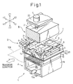
- FIG. 1 is a partially cutaway perspective view of main parts of a partial plating system according to the present invention.
- the partial plating system 1 is comprised generally of a mask I, an elevator/guide unit II (elevating means), and a press unit III (pressing means). Further, the TAB tape 106 is transported to the partial plating system 1 in the state with its surface in a horizontal plane (called “horizontal transport” hereinafter). Note that the large arrow in the figure shows the direction of transport of the TAB tape 106. This matches with the longitudinal direction of the TAB tape 106.
- the above mask I is provided with a mask jig 9 made of rubber or another elastomer. Further, this mask jig 9 is provided with a plurality of openings 9a, 9a... formed corresponding to plating regions of the TAB tape 106 and demarcating the plating regions.
- the "plating regions” means regions of the TAB tape 106 (see FIG. 13A) which require gold plating. Specifically, they are the substantially rectangular regions including the inner leads 102a inside them. The shapes and sizes substantially match those of the device holes 104.
- Cathode feed plates 10, 10 connected to a not shown power source are provided at the two sides of the mask jig 9.
- the cathode feed plates 10, 10 contact the copper foil leads 102 (see FIGS. 13A and 13B) to be plated on the TAB tape 106 and use the copper foil leads 102 as cathodes.
- the cathode feed plates 10, 10 are provided with guide pins 12, 12... for entering sprocket holes 103 (engagement holes) of the TAB tape 106 (see FIG. 13A).
- a plurality of the guide pins 12, 12... are provided on the cathode feed plates 10, 10 at predetermined intervals in the transport direction (X1-X2 direction) so as correspond to the sprocket holes 103 (in FIG. 1, two of these are visible).
- the guide pins 12, 12... function to position the plating regions of the TAB tape 106 and the openings 9a of the mask jig 9 with respect to each other by engagement with the sprocket holes 103.
- the mask jig 9 and the cathode feed plates 10, 10 are screwed to a holding plate 13.
- the holding plate 13 and the mask jig 9 and cathode feed plates 10, 10 constitute the mask I.
- the mask I is placed on a base member 14 so as to be able to slide around a predetermined reference position in the horizontal plane (X1-Y1 plane). This point will be explained with reference to FIG. 2A and FIG. 2B.
- FIG. 2A and FIG. 2B are enlarged sectional views of the mask I and the base member 14 seen from the transport direction.
- the cathode feed plates 10 and the holding plate 13 are formed with through holes 21.
- a threaded hole 14a communicating with the through holes 21 is provided in the base member 14 below the through holes 21.
- a mask fastening bolt 11 is passed through the through holes 21, then the threaded part of the mask fastening bolt 11 is screwed into the threaded hole 14a.
- a plurality of mask fastening bolts 11 are provided at predetermined intervals in the transport direction.
- the diameter of the head of the mask fastening bolt 11 is larger than the diameter D2 of the through holes 21. Due to this, the movement of the mask I in the vertical direction is limited.
- the diameter D1 of the threaded part of the mask fastening bolt 11 is smaller than the diameter D2 of the through holes 21, so a clearance is formed between the circumference of the mask fastening bolt 11 and the through holes 21. Therefore, the mask I can freely move in the horizontal direction by exactly that clearance. In other words, the mask I is placed on the base member 14 so as to be able to slide around the position of the mask fastening bolts 11 (reference positions).
- an anodic nozzle plate 22 comprised of a protective plate 16 and an anodic plate 17 are provided below the mask I.
- a polyvinyl chloride plate is used as the protective plate 16.
- a stainless steel plate is used as the anodic plate 17.
- the anodic plate 17 functions as the anode at the time of electroplating.
- the protective plate 16 functions to prevent the plating solution rising from below from directly contacting the anodic plate 17 and corroding the anodic cathode plate 17.
- nozzles 15, 15... are provided on the anodic nozzle plate 22 at positions corresponding to the openings 9a of the mask jig 9.
- the plating solution rises through these nozzles 15, 15... and is sprayed from the front ends to the plating surfaces of the TAB tape 106.
- the plating solution may be sprayed to only the portions of the TAB tape exposed from the openings 9a, so the nozzles 15, 15... may be arranged in accordance with the size and shape of the openings 9a.
- four nozzles 15, 15... are provided for one opening 9a (in FIG. 1, only two of the four are visible).
- polyvinyl chloride pipes may be used as the nozzles 15, 15...
- an orifice plate 18 formed with a plurality of orifices 18a, 18a... These orifices 18a, 18a,... function to make the flow of the plating solution rising from below uniform to make the spraying of the plating solution from the nozzles 15 uniform. Due to this, it is possible to plate the TAB tape 106 to obtain a uniform plating thickness.
- the orifice plate 18 is housed in a sparger tank 19. At the bottom of the sparger tank 19 is formed a plating solution feed port 19a for supplying plating solution to the inside.
- an elevator/guide unit II comprised of a plurality of support pieces 8, 8... and connecting rods 6, 6 for connecting these by screws 7, 7...
- the front ends of the support pieces 8, 8... are provided with guide grooves 8a for receiving the peripheral edges of the TAB tape 106 and guiding the TAB tape in the transport direction.
- a plurality of support pieces 8, 8... are arranged at predetermined intervals in the transport direction.
- the elevator/guide unit II is connected to an actuator (not shown) driven to elevate and descend in the vertical direction and can therefore be elevated or lowered in the vertical direction. Further, the TAB tape 106 is also made to elevate and lower in the vertical direction along with the motion of the elevator/guide unit II.
- a press unit III comprised of a press block 2 and a backing 3.
- an upper chassis 20 and actuator 4 provided at the same. Note that the upper chassis 20 is fastened to a not shown housing of the partial plating system 1.
- the actuator 4 is connected to one end of an elevation shaft 5.
- the other end of the elevation shaft 5 is connected to the press block 2.
- the actuator 4 drives the elevation shaft 5 to rise or descend in the vertical direction and thereby drive the press unit III to rise or descend in the vertical direction.
- the backing 3 functions to press the back of the TAB tape 106 (side opposite to plating surface) so that the plating surface of the TAB tape 106 is pressed against the mask jig 9 when the press unit III is lowered (Z2 direction). If the mask jig 9 is pressed against so that no clearance is formed between the plating surface of the TAB tape 106 and the mask jig 9, it will be possible to prevent entry of the plating solution to portions of the TAB tape 106 other than the plating regions. In particular, if an elastomer is used as the backing 3, the TAB tape 106 can be pressed against the mask jig 9 as desired.
- the backing 3 is made of silicone rubber or another rubber, a sponge, etc.
- FIG. 3 is a functional block diagram of the partial plating system 1 according to the present embodiment.
- the controller 23 shown in FIG. 3 controls the actuator 4 or the actuator for driving the vertical motion of the elevator/guide unit II (not shown) and thereby controls the movement of the elevator/guide unit II and the press unit III.
- the TAB tape 106 is fed into the partial plating system 1 by a tape feeder 24 (feeding means) shown in FIG. 3.
- the tape feeder 24 is controlled by the controller 23 to feed exactly a certain length of the TAB tape 106 in the transport direction. When that length finishes being plated, a new same length of the TAB tape 106 is fed to the partial plating system 1.
- the tape feeder 24 intermittently feeds the TAB tape 106, and that length of the TAB tape 106 is plated by a single plating operation.
- FIG. 4 is a sectional view of the partial plating system 1 viewed from the side A of FIG. 1.
- a guide shaft 24 is fixed to the press block 2. This guide shaft 24 is inserted through a guide hole 20a of the upper chassis 20. This guide shaft 24 guides the upward and downward movement of the press block so that the press block does not tilt.
- the rear end of the press block 2 is formed with a positioning hole 2a in which a backing positioning pin 25 provided at the base member 14 can enter.
- a backing positioning pin 25 provided at the base member 14 can enter.
- the solid arrows in FIG. 4 show the flow of the plating solution.
- the plating solution is first pumped from the plating solution feed port 19a to the inside of the sparger tank 19. Next, it is pumped up by a not shown pump, passes through the orifice plate 18, and is sprayed from the front ends of the nozzles 15. The sprayed plating solution proceeds next toward the right in the figure (X1 direction) and finally is discharged to the outside from the plating solution discharge port 19. Next, the plating solution discharged to the outside is again transported to the plating solution pumping port 19a by a not shown pump and supplied into the partial plating system 1 again from there.
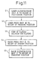
- FIG. 5 to FIG. 10 are sectional views of the partial plating system 1 performing the plating as seen from the transport direction. Note that in these figures, members which do not have to be explained below are omitted. Further, FIG. 11 is a flow chart of the plating operation of the partial plating system 1.
- the entire system is in the state shown in FIG. 5.
- the press unit III is highest in position. Below, this height position of the press unit III will be called the "standby position".
- the elevator/guide unit II is at the height position where the TAB tape 106 is transported toward the transport direction. At this height position, the TAB tape 106 can move freely in the transport direction without interference with the mask I or the press unit III. Below, this height position of the elevator/guide unit II will be called the "transport position".
- the elevator/guide unit II is lowered downward (Z2 direction) (step S1). Due to this, the TAB tape 106 is lowered downward and the guide pins 12 enter the sprocket holes 103 (see FIG. 13A). At this time, the guide pins 12 contact the inside walls of the sprocket holes 103 and the TAB tape 106 and the mask jig 9 are corrected in position so that the plating regions of the TAB tape 106 come into register with the openings 9a of the mask jig 9. In other words, in the step shown in FIG. 6, the plating regions of the TAB tape 106 and the openings 9a of the mask jig 9 are positioned with respect to each other. The height position of the elevator/guide unit II at this time will be called the "positioning position" below.
- the mask I is placed on the base member 14 so as to be able to slide around the positions of the mask fastening bolts 11 (reference positions). Therefore, in this process, the positions of not only the TAB tape 106, but also the mask I are corrected so that the plating regions and the openings come into register.
- the present inventor discovered that by enabling the mask I to slide in this way, the length of the TAB tape 106 plated in a single plating operation can be increased over the case where the mask I cannot slide. This will be explained below.
- the force acting between them is released by the TAB tape 106 and the mask I shifting in position in the horizontal plane.
- the force acting on the TAB tape 106 becomes smaller than the case where the mask I cannot slide due to the mask I shifting in the horizontal plane. Therefore, in this case, the force acting on a unit length of the TAB tape 106 becomes smaller than the case where the mask I cannot slide.
- the force acting on the TAB tape 106 becomes larger the longer the length of the TAB tape 106 transported to the partial plating system (length plated by a single plating operation).
- the force acting on the TAB tape 106 is preferably kept as small as possible to prevent deformation of the TAB tape 106.
- the force acting on the TAB tape 106 can be kept small even if increasing the length of the TAB tape 106 being plated by a single plating operation. That is, in the present embodiment, the length of the TAB tape plated by a single plating operation can be increased compared with the case where the mask I cannot slide.
- the length of the TAB tape which can be plated by a single plating operation becomes about twice that of the case where the mask I cannot slide. Due to this, the throughput of the partial plating system 1 can be improved over the case where the mask I cannot slide.
- step S2 the process shown in FIG. 7 (step S2) is performed.
- the press unit III in the standby position is lowered to press against the back of the TAB tape 106 by the backing 3. Below, this height position of the press unit III will be called the "pressing position".
- the TAB tape 106 and the mask jig 9 positioned at step S1 are pressed together and the plating regions of the TAB tape 106 are demarcated by the openings 9a of the mask jig 9.
- the plating solution is pumped up and sprayed from the nozzles 15 (step S3). Due to this, the plating solution is sprayed at the plating regions of the TAB tape 106 exposed from the openings 9a of the mask jig 9 and the plating regions are gold plated. At this time, portions of the TAB tape 106 other than the plating regions are covered by the mask jig 9, so the portions other than the plating regions will not be plated unlike in the past. Therefore, with recycling, there is no wasteful use of expensive gold and the cost of the plating process can be reduced.
- the plating solution will not flow over the surface of the plating regions after being sprayed, the amount of the plating solution deposited will become uniform in the plating regions, and therefore the plating thickness can be made uniform.
- step S4 the press unit III is made to rise to stand by at that height position.
- the TAB tape 106 and the mask jig 9 are in close contact due to the surface tension of the plating solution remaining between them.
- step S5 the elevator/guide unit II is made to rise to the height of the transport position. Due to this, the closely contacting TAB tape 106 and mask jig 9 are separated. Next, the steps shown in FIG. 5 to FIG. 10 are repeated.
- the elevator/guide unit II is driven to rise and descend by a not shown actuator, but the present embodiment is not limited to this.
- similar actions and effects as the above are exhibited even when using an elevator/guide unit II shown in FIG. 12.
- springs 26 biasing members
- these springs 26 bias the elevator/guide unit II in the direction to move away from the base member. Note that when using such an elevator/guide unit II, projections 2b are provided at the press block 2.
- the elevator/guide unit II when lowering the press unit III downward, the projections 2b abut against the support pieces 8 whereby the support pieces 8 are pressed downward. Therefore, no actuator is needed for driving the elevator/guide unit II to rise or descend. Therefore, the cost of production of the partial plating system 1 can be reduced by the amount of that actuator. Further, along with this, it is possible to simultaneously perform the step shown in FIG. 9 and the step shown in FIG. 10. That is, if the press unit III is made to rise as shown in FIG. 9, the elevator/guide unit II is made to naturally rise to the transport position by the elastic force of the springs 26 and the TAB tape 106 and mask jig 9 are separated. Due to this, if the elevator/guide unit II shown in FIG. 12 is used, it is possible to simplify the plating process.
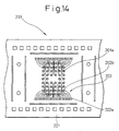
- the TAB tape of the present embodiment includes a tape 203 for a tape ball grid array (BGA) as shown in FIG. 14 in addition to the TAB tape 106 shown in FIG. 13A.
- BGA tape ball grid array
- a copper foil bonded to a polyimide film 201 is patterned to form a wiring pattern 202.
- the polyimide film 201 is formed with through holes 201a, 201a... Pads 202b, 202b,... of the wiring pattern are formed at the open ends of the through holes 201a, 201a,...
- the pads 202b, 202b,... are connected to solder bumps for forming the external connection terminals through the through holes 201a, 201a,...
- the mounted semiconductor element (not shown) is then wire bonded by the wire bonding parts 202a, 202a,... of the wiring pattern 202 and the gold wires. Then, the partial plating system 1 of the present embodiment is used to partially plate the wire bonding parts 202a, 202a... with gold.
- the mask by placing the mask on a base member so as to be able to slide in a horizontal plane around a predetermined reference position, it is possible to ease the force acting on the TAB tape at the time of positioning. Due to this, it is possible to increase the length of the TAB tape plated by a single plating operation compared with the case where the mask cannot slide.
Landscapes
- Chemical & Material Sciences (AREA)
- Engineering & Computer Science (AREA)
- Chemical Kinetics & Catalysis (AREA)
- Electrochemistry (AREA)
- Materials Engineering (AREA)
- Metallurgy (AREA)
- Organic Chemistry (AREA)
- Electroplating Methods And Accessories (AREA)
- Wire Bonding (AREA)
- Manufacturing Of Printed Wiring (AREA)
- Lead Frames For Integrated Circuits (AREA)
Abstract
Description
Claims (6)
- A plating system provided with:a mask (9) having an opening (9a) formed to correspond to a partial region of a TAB tape to be plated and provided substantially horizontally;an elevating means (II) for, in use, lowering said TAB tape toward said mask; and,a pressing means (III) for, in use, pressing the TAB tape on to said mask (9);in use, a plating solution being sprayed from below said opening (9a) toward said opening to plate said plating region.
- A plating system according to claim 1, wherein said mask (9) is provided on its surface with guide pins (12) for engagement with engagement holes of said TAB tape and is placed on a base member (14) so as to be able to slide in a horizontal plane around a predetermined reference position.
- A plating system according to claim 2, wherein a biasing member (26) is provided between said elevating means (II) and said base member (14) and wherein said elevating means (II) is biased to move away from said base member (14).
- A plating system according to any one of claims 1 to 3, further provided with a feed means for transporting said TAB tape in a longitudinal direction by exactly a predetermined length after the plating system plates a certain length of the TAB tape in one plating operation.
- A plating system according to any one of claims 1 to 4, wherein said elevating means (II) is provided with a guide means for use when said TAB tape is being transported in said longitudinal direction.
- A plating system according to any one of the preceding claims, wherein said TAB tape is replaced with a lead frame.
Applications Claiming Priority (2)
| Application Number | Priority Date | Filing Date | Title |
|---|---|---|---|
| JP2000128375 | 2000-04-27 | ||
| JP2000128375A JP3553461B2 (en) | 2000-04-27 | 2000-04-27 | Partial plating equipment |
Publications (2)
| Publication Number | Publication Date |
|---|---|
| EP1149936A2 true EP1149936A2 (en) | 2001-10-31 |
| EP1149936A3 EP1149936A3 (en) | 2002-11-27 |
Family
ID=18637827
Family Applications (1)
| Application Number | Title | Priority Date | Filing Date |
|---|---|---|---|
| EP01303683A Withdrawn EP1149936A3 (en) | 2000-04-27 | 2001-04-23 | Plating system |
Country Status (6)
| Country | Link |
|---|---|
| US (1) | US6656275B2 (en) |
| EP (1) | EP1149936A3 (en) |
| JP (1) | JP3553461B2 (en) |
| KR (1) | KR20010098834A (en) |
| CN (1) | CN1250776C (en) |
| TW (1) | TWI237069B (en) |
Cited By (2)
| Publication number | Priority date | Publication date | Assignee | Title |
|---|---|---|---|---|
| WO2003060201A1 (en) * | 2001-12-28 | 2003-07-24 | Huebel Egon | System and method for items to be electrochemically treated |
| RU2630996C1 (en) * | 2016-11-10 | 2017-09-15 | Федеральное государственное бюджетное образовательное учреждение высшего образования "Российский химико-технологический университет имени Д.И. Менделеева" | Device for local application of metal coatings by electrolytic method |
Families Citing this family (21)
| Publication number | Priority date | Publication date | Assignee | Title |
|---|---|---|---|---|
| JP4130352B2 (en) | 2002-03-29 | 2008-08-06 | Dowaホールディングス株式会社 | Wet processing method for base-integrated metal ceramic bonding member, power module member and power module manufactured by the wet processing method |
| US7407738B2 (en) * | 2004-04-02 | 2008-08-05 | Pavel Kornilovich | Fabrication and use of superlattice |
| CN1296522C (en) * | 2004-07-14 | 2007-01-24 | 林少伟 | Parcel plating process and local gold plating special machine for hardware |
| US7375012B2 (en) * | 2005-02-28 | 2008-05-20 | Pavel Kornilovich | Method of forming multilayer film |
| JP4915220B2 (en) * | 2006-11-24 | 2012-04-11 | 富士通株式会社 | Mobile terminal device |
| US7799182B2 (en) * | 2006-12-01 | 2010-09-21 | Applied Materials, Inc. | Electroplating on roll-to-roll flexible solar cell substrates |
| US20080128019A1 (en) * | 2006-12-01 | 2008-06-05 | Applied Materials, Inc. | Method of metallizing a solar cell substrate |
| US20100126849A1 (en) * | 2008-11-24 | 2010-05-27 | Applied Materials, Inc. | Apparatus and method for forming 3d nanostructure electrode for electrochemical battery and capacitor |
| US9025285B1 (en) | 2009-12-16 | 2015-05-05 | Magnecomp Corporation | Low resistance interface metal for disk drive suspension component grounding |
| US9583125B1 (en) | 2009-12-16 | 2017-02-28 | Magnecomp Corporation | Low resistance interface metal for disk drive suspension component grounding |
| WO2012085682A2 (en) * | 2010-12-23 | 2012-06-28 | Fci | Plating method and apparatus, and strip obtained by this method |
| DE102016112289B4 (en) * | 2016-07-05 | 2020-07-30 | Danfoss Silicon Power Gmbh | Lead frame and method of making the same |
| CN107385491B (en) * | 2017-07-11 | 2019-02-01 | 宁波启谱自动化科技有限公司 | Silver plating machine is electroplated in IC lead frame chip |
| TWI612180B (en) * | 2017-07-19 | 2018-01-21 | Triumphant Gate Ltd | Continuous purification system for chemical displacement gold plating solution and impurity nickel and impurity copper |
| CN107705945B (en) * | 2017-09-25 | 2019-07-19 | 江苏时恒电子科技有限公司 | A kind of preparation method of thermistor copper electrode and its press seal mold used |
| CN107946201B (en) * | 2017-12-19 | 2020-03-31 | 哈尔滨工业大学 | Preparation method of lead bonding welding spot structure based on local electrodeposition |
| CN114698256B (en) * | 2020-12-30 | 2024-08-09 | 深南电路股份有限公司 | Manufacturing method of circuit board, circuit board and electronic device |
| CN114892248B (en) * | 2022-06-01 | 2024-01-26 | 北京半导体专用设备研究所(中国电子科技集团公司第四十五研究所) | Electroplating clamp |
| CN115863181B (en) * | 2022-11-25 | 2024-06-21 | 崇辉半导体(江门)有限公司 | Selective roughening equipment and roughening method for semiconductor lead frame |
| KR102638387B1 (en) * | 2023-09-22 | 2024-02-20 | 주식회사 이피코리아 | Partial plating device |
| KR102690580B1 (en) * | 2023-12-26 | 2024-07-31 | 주식회사 이피코리아 | Cathode connection device for partial plating |
Family Cites Families (16)
| Publication number | Priority date | Publication date | Assignee | Title |
|---|---|---|---|---|
| JPS5512112B2 (en) * | 1973-02-23 | 1980-03-29 | ||
| US3860499A (en) * | 1973-04-19 | 1975-01-14 | Gte Sylvania Inc | Electroplating apparatus and method |
| US3974056A (en) * | 1975-05-23 | 1976-08-10 | Ann Arbor Circuits, Inc. | Electroplating selected portions of a strip |
| US4163704A (en) * | 1975-06-14 | 1979-08-07 | Electroplating Engineers Of Japan, Ltd. | Apparatus for selectively plating rectangular sheet continuously or intermittently |
| US4367125A (en) * | 1979-03-21 | 1983-01-04 | Republic Steel Corporation | Apparatus and method for plating metallic strip |
| JPS60255992A (en) | 1984-06-01 | 1985-12-17 | Shinko Electric Ind Co Ltd | Partial plating apparatus |
| JPS60260142A (en) | 1984-06-06 | 1985-12-23 | Shinko Electric Ind Co Ltd | Lead frame |
| JPS61177391A (en) | 1985-01-31 | 1986-08-09 | Sumitomo Metal Mining Co Ltd | Annular part plating apparatus |
| JPS62156290A (en) * | 1985-12-27 | 1987-07-11 | Sumitomo Electric Ind Ltd | Mask device for spotting |
| JP2537762B2 (en) | 1987-04-02 | 1996-09-25 | 新光電気工業株式会社 | Partial plating device |
| JP2666415B2 (en) * | 1988-10-18 | 1997-10-22 | 松下電器産業株式会社 | Partial plating equipment |
| JPH05125583A (en) * | 1991-11-07 | 1993-05-21 | Sumitomo Metal Mining Co Ltd | Jet partial plating device and partial plating method for lead frame using this device |
| JP3339926B2 (en) | 1993-08-11 | 2002-10-28 | 新光電気工業株式会社 | Partial plating equipment |
| US6132798A (en) * | 1998-08-13 | 2000-10-17 | Micron Technology, Inc. | Method for applying atomized adhesive to a leadframe for chip bonding |
| JP3093973B2 (en) * | 1996-05-27 | 2000-10-03 | 松下電子工業株式会社 | Partial plating method and equipment for strip material |
| JP3451391B2 (en) * | 1998-03-11 | 2003-09-29 | 株式会社三井ハイテック | Plating equipment |
-
2000
- 2000-04-27 JP JP2000128375A patent/JP3553461B2/en not_active Expired - Fee Related
-
2001
- 2001-04-23 EP EP01303683A patent/EP1149936A3/en not_active Withdrawn
- 2001-04-24 KR KR1020010022007A patent/KR20010098834A/en not_active Withdrawn
- 2001-04-24 US US09/841,224 patent/US6656275B2/en not_active Expired - Fee Related
- 2001-04-26 TW TW090110011A patent/TWI237069B/en not_active IP Right Cessation
- 2001-04-27 CN CNB011171685A patent/CN1250776C/en not_active Expired - Fee Related
Cited By (2)
| Publication number | Priority date | Publication date | Assignee | Title |
|---|---|---|---|---|
| WO2003060201A1 (en) * | 2001-12-28 | 2003-07-24 | Huebel Egon | System and method for items to be electrochemically treated |
| RU2630996C1 (en) * | 2016-11-10 | 2017-09-15 | Федеральное государственное бюджетное образовательное учреждение высшего образования "Российский химико-технологический университет имени Д.И. Менделеева" | Device for local application of metal coatings by electrolytic method |
Also Published As
| Publication number | Publication date |
|---|---|
| TWI237069B (en) | 2005-08-01 |
| US6656275B2 (en) | 2003-12-02 |
| EP1149936A3 (en) | 2002-11-27 |
| JP2001303297A (en) | 2001-10-31 |
| US20010036514A1 (en) | 2001-11-01 |
| JP3553461B2 (en) | 2004-08-11 |
| CN1326016A (en) | 2001-12-12 |
| KR20010098834A (en) | 2001-11-08 |
| CN1250776C (en) | 2006-04-12 |
Similar Documents
| Publication | Publication Date | Title |
|---|---|---|
| US6656275B2 (en) | Partial plating system | |
| US6774467B2 (en) | Semiconductor device and process of production of same | |
| US7830667B2 (en) | Flexible wiring substrate and method for producing the same | |
| CN102365737B (en) | Manufacturing method of substrate for semiconductor element and semiconductor device | |
| US20020027294A1 (en) | Electrical component assembly and method of fabrication | |
| EP2158617B1 (en) | Light emitting device package and manufacturing method thereof | |
| US8373262B2 (en) | Source driver, method for manufacturing same, and liquid crystal module | |
| SG175042A1 (en) | Method for manufacturing substrate for semiconductor element, and semiconductor device | |
| EP4312249A1 (en) | Pin fin placement assembly for forming temperature control element utilized in device die packages | |
| US7880308B2 (en) | Semiconductor device | |
| JPH03250756A (en) | Outer lead molding process of semiconductor element | |
| US20110133319A1 (en) | Auxiliary leadframe member for stabilizing the bond wire process | |
| JP3181229B2 (en) | Semiconductor device, its manufacturing method, its mounting method, and lead frame and its manufacturing method | |
| KR101644444B1 (en) | Soldering device for regulator | |
| KR102690580B1 (en) | Cathode connection device for partial plating | |
| KR102638387B1 (en) | Partial plating device | |
| KR100274931B1 (en) | Pressure Box Assembly of Plating Equipment for Semiconductor Lead Frames | |
| CN119208204B (en) | Electronic packaging equipment | |
| CN211331084U (en) | Bending device capable of bending lead frame pins of various models | |
| KR101141704B1 (en) | Method for manufacturing a lead frame and press system for the same | |
| KR20250040420A (en) | Apparatus and method for manufacturing lead frame including grooved lead | |
| JP2666415B2 (en) | Partial plating equipment | |
| JPH039893A (en) | Printed wiring board for ic card | |
| KR20000030786A (en) | A pin-hole alignment device for a apparatus for plating leadframe | |
| KR20030058405A (en) | Apparatus for plating lead frame and process for plating lead frame using the same |
Legal Events
| Date | Code | Title | Description |
|---|---|---|---|
| PUAI | Public reference made under article 153(3) epc to a published international application that has entered the european phase |
Free format text: ORIGINAL CODE: 0009012 |
|
| AK | Designated contracting states |
Kind code of ref document: A2 Designated state(s): AT BE CH CY DE DK ES FI FR GB GR IE IT LI LU MC NL PT SE TR |
|
| AX | Request for extension of the european patent |
Free format text: AL;LT;LV;MK;RO;SI |
|
| PUAL | Search report despatched |
Free format text: ORIGINAL CODE: 0009013 |
|
| AK | Designated contracting states |
Kind code of ref document: A3 Designated state(s): AT BE CH CY DE DK ES FI FR GB GR IE IT LI LU MC NL PT SE TR |
|
| AX | Request for extension of the european patent |
Free format text: AL;LT;LV;MK;RO;SI |
|
| 17P | Request for examination filed |
Effective date: 20030516 |
|
| AKX | Designation fees paid |
Designated state(s): NL |
|
| REG | Reference to a national code |
Ref country code: DE Ref legal event code: 8566 |
|
| 17Q | First examination report despatched |
Effective date: 20040618 |
|
| GRAP | Despatch of communication of intention to grant a patent |
Free format text: ORIGINAL CODE: EPIDOSNIGR1 |
|
| STAA | Information on the status of an ep patent application or granted ep patent |
Free format text: STATUS: THE APPLICATION IS DEEMED TO BE WITHDRAWN |
|
| 18D | Application deemed to be withdrawn |
Effective date: 20110210 |