EP1148652A2 - Digital-signal receiving apparatus - Google Patents
Digital-signal receiving apparatus Download PDFInfo
- Publication number
- EP1148652A2 EP1148652A2 EP01303476A EP01303476A EP1148652A2 EP 1148652 A2 EP1148652 A2 EP 1148652A2 EP 01303476 A EP01303476 A EP 01303476A EP 01303476 A EP01303476 A EP 01303476A EP 1148652 A2 EP1148652 A2 EP 1148652A2
- Authority
- EP
- European Patent Office
- Prior art keywords
- data
- processing
- types
- calculation
- information indicating
- Prior art date
- Legal status (The legal status is an assumption and is not a legal conclusion. Google has not performed a legal analysis and makes no representation as to the accuracy of the status listed.)
- Granted
Links
Images


Classifications
-
- H—ELECTRICITY
- H04—ELECTRIC COMMUNICATION TECHNIQUE
- H04W—WIRELESS COMMUNICATION NETWORKS
- H04W52/00—Power management, e.g. Transmission Power Control [TPC] or power classes
- H04W52/02—Power saving arrangements
- H04W52/0209—Power saving arrangements in terminal devices
- H04W52/0261—Power saving arrangements in terminal devices managing power supply demand, e.g. depending on battery level
- H04W52/0274—Power saving arrangements in terminal devices managing power supply demand, e.g. depending on battery level by switching on or off the equipment or parts thereof
- H04W52/028—Power saving arrangements in terminal devices managing power supply demand, e.g. depending on battery level by switching on or off the equipment or parts thereof switching on or off only a part of the equipment circuit blocks
-
- Y—GENERAL TAGGING OF NEW TECHNOLOGICAL DEVELOPMENTS; GENERAL TAGGING OF CROSS-SECTIONAL TECHNOLOGIES SPANNING OVER SEVERAL SECTIONS OF THE IPC; TECHNICAL SUBJECTS COVERED BY FORMER USPC CROSS-REFERENCE ART COLLECTIONS [XRACs] AND DIGESTS
- Y02—TECHNOLOGIES OR APPLICATIONS FOR MITIGATION OR ADAPTATION AGAINST CLIMATE CHANGE
- Y02D—CLIMATE CHANGE MITIGATION TECHNOLOGIES IN INFORMATION AND COMMUNICATION TECHNOLOGIES [ICT], I.E. INFORMATION AND COMMUNICATION TECHNOLOGIES AIMING AT THE REDUCTION OF THEIR OWN ENERGY USE
- Y02D30/00—Reducing energy consumption in communication networks
- Y02D30/70—Reducing energy consumption in communication networks in wireless communication networks
Definitions
- the present invention relates to receivers for digital broadcasting.
- DAB Digital Audio Broadcasting
- Eureka European Research Coordinating Agency
- DAB various encoding processes are applied to a plurality of digital data items to convert them finally to an orthogonal-frequency-division-multiplex (OFDM) signal, and a main carrier signal is differential-quadrature-phase-shift-keying (D-QPSK) modulated by the OFDM signal to form a transmission signal.
- D-QPSK differential-quadrature-phase-shift-keying
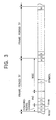
- Fig. 3 shows the structure of the OFDM signal in the time domain.
- the OFDM signal is formed of a plurality of frames. Each frame is formed of (m + 1) symbols.
- DAB has four transmission mode. In mode II, for example, the time length of a frame is 24 ms and the number (m + 1) of symbols is 76.
- Each frame is divided into a synchronizing channel SC, a fast information channel FIC, and a main service channel MSC, with symbols being used as units.
- the synchronizing channel SC is used for processing, such as frame synchronization and automatic frequency control (AFC), in receivers.
- AFC automatic frequency control
- the synchronizing channel SC is formed of two symbols, the first symbol thereof is a null symbol NULL, and the second symbol thereof is a symbol TFPR used for phase reference.
- the fast information channel FIC is used for providing data related to the main service channel MSC, and includes data, such as the time, the date, a type, a data arrangement, and traffic and message control data.
- the main service channel MSC includes digital audio data and various digital data items serving as main data.
- DAB receivers need to perform signal processing, such as orthogonal demodulation, fast Fourier transform (FFT), OFDM demodulation, deinterleaving, error correction, and digital-to-analog (D/A) conversion, in response to signal processing performed at a transmitting side.
- signal processing such as orthogonal demodulation, fast Fourier transform (FFT), OFDM demodulation, deinterleaving, error correction, and digital-to-analog (D/A) conversion, in response to signal processing performed at a transmitting side.
- FFT fast Fourier transform
- OFDM demodulation OFDM demodulation
- deinterleaving deinterleaving
- error correction error correction
- D/A digital-to-analog
- the present invention has been made in consideration of the following condition. It is an object of the present invention to allow the DSP for processing digital sound broadcasting (DSB) data to enter a sleep state to reduce power consumption.
- DSP digital sound broadcasting
- a receiving apparatus for receiving a signal having a plurality of types of data in each frame period, including a plurality of accumulation means for accumulating the plurality of types of data, respectively, in each frame period; at least one calculation-processing means for processing each of the plurality of types of data accumulated by the plurality of accumulation means; and storage means for storing information indicating that each of the plurality of types of data has been accumulated into accumulation means, wherein the calculation-processing means applies processing to data accumulated into accumulation means, corresponding to information indicating the completion of data accumulation stored in the storage means.
- calculation processing starts with data which has been accumulated among the plurality of types of data, each processing is sequentially performed from the beginning of a frame period, a period is formed near the end point of the frame period, in which the calculation-processing means can enter, for example, a sleep mode.
- the receiving apparatus may be configured such that the storage means further stores information indicating the order of priority in which processing is applied to each of the plurality of types of data, and the calculation-processing means applies processing to the plurality of types of data in the order of priority.
- calculation-processing means when the calculation-processing means is ready to start processing, if two or more data items need to be processed, data processing is performed in an appropriate order according to the order of priority.
- the receiving apparatus may be configured such that the storage means further stores information indicating the completion of processing applied to each of the plurality of types of data, and the calculation-processing means enters a sleep state when all processing applied to the plurality of types of data has been completed.
- the calculation-processing means since it is positively checked that all processing applied to the data has been completed, before the calculation-processing means enters a sleep state in a sleep period formed near the end point of a frame period, the calculation-processing means enters the sleep state without any problems.
- the receiving apparatus may be configured such that the storage means further stores information indicating that corresponding data is allowed to be processed, and the calculation-processing means applies processing to data for which data processing is allowed among the plurality of types of data.
- a sleep period can be formed near the end point of a frame period.
- a receiving apparatus for receiving a signal having a plurality of types of data in each frame period, including a plurality of accumulation means for accumulating the plurality of types of data, respectively, in each frame period; at least one calculation-processing means for processing each of the plurality of types of data accumulated by the plurality of accumulation means; and storage means for storing information indicating that each of the plurality of types of data has been processed; wherein the calculation-processing means enters a sleep state when all processing applied to the plurality of types of data has been completed, according to the information indicating the completion of processing.
- a receiving apparatus for receiving a signal having a plurality of types of data in each frame period, including a plurality of accumulation means for accumulating the plurality of types of data, respectively, in each frame period; at least one calculation-processing means for processing each of the plurality of types of data accumulated by the plurality of accumulation means; and storage means for storing information indicating that each of the plurality of types of data is allowed to be processed; wherein the calculation-processing means applies processing to data accumulated into the accumulation means corresponding to the storage means for storing information indicating that data is allowed to be processed.
- a receiving apparatus for receiving a signal having a plurality of types of data in each frame period, including a plurality of accumulation means for accumulating the plurality of types of data, respectively, in each frame period; at least one calculation-processing means for processing each of the plurality of types of data accumulated by the plurality of accumulation means; and storage means for storing information indicating that each of the plurality of types of data is allowed to be processed, information indicating that each of the plurality of types of data has been accumulated into accumulation means, information indicating the order of priority given to each of the plurality of types of data, and information indicating the completion of processing applied to each of the plurality of types of data, wherein the calculation-processing means performs data processing in the order of priority given to each data when a plurality of data corresponding to information indicating that data processing is allowed has been accumulated into the accumulation means, and the calculation-processing means enters a sleep state when all processing applied to the plurality of data has
- a tuner circuit 10 for receiving DAB an integrated circuit (IC) 20, and a microcomputer 40 for system control.
- IC integrated circuit
- the tuner circuit 10 uses a superheterodyne method and a synthesizer method, converts in frequency a target broadcasting signal to an intermediate-frequency signal (an intermediate frequency is set, for example, to 3.072 megahertz (MHz)) among broadcasting signals received by an antenna 11, and sends it to the IC 20.
- an intermediate frequency is set, for example, to 3.072 megahertz (MHz)
- the IC 20 takes the audio signal of a target program out of the received intermediate-frequency signal. Circuits 21 to 37 surrounded by a chain line are integrated into the IC 20.
- the microcomputer 40 is connected to the IC 20, and is also connected to various operation keys (operation switches) 41.
- the intermediate-frequency signal sent from the tuner circuit 10 is input to an analog-to-digital (A/D) converter circuit 21, and is converted to a digital signal.
- the digital signal is sent to an orthogonal demodulation circuit 22, and the data of an in-phase component and orthogonal components (real-axis component and imaginary-axis component) is demodulated.
- Complex Fourier conversion is applied to demodulated data by an FFT circuit 23, and frequency components are output in units of symbols.
- the frequency components are input to a Viterbi decoder 24, deinterleaving and error correction are applied to the components, and the target program is selected to select the digital audio data of the target program.
- the digital audio data of the selected program is sent to a main bus 31 through a buffer circuit 25.
- the main bus 31 is connected to a main-bus controller 32.
- the main-bus controller 32 controls data flow between the main bus 31 and circuits connected to the main bus 31, and achieves data access between the microcomputer 40 and circuits 35 and 36, described later.
- the digital audio data sent to the main bus 31 through the buffer circuit 25 is further sent to a DSP 26.
- the DSP 26 includes a central processing unit (CPU) 261, a memory 262 to which a program to be executed by the CPU 261 and data are loaded, a universal asynchronous receiver/transmitter (UART) 263 for achieving data access to an external device, and a power-management circuit 264.
- the CPU 261 has an arithmetic and logic unit (ALU) for executing arithmetic calculations (not including multiplications) and logical calculations, and a multiply and accumulate (MAC) unit for executing sum-of-products calculations.
- ALU arithmetic and logic unit
- MAC multiply and accumulate
- the DSP 26 executes Motion-Picture-Image-Coding-Experts-Group (MPEG) audio decoding processing, and therefore, outputs decompressed data, that is, the original digital audio data.
- MPEG Motion-Picture-Image-Coding-Experts-Group
- the DSP 26 sends the digital audio data through the main bus 31, and further through a buffer circuit 27 to a D/A converter circuit 28.
- the D/A converter circuit 28 converts the data to analog audio signals AL and AR, and sends them to a terminal 29A.
- the digital audio data sent to the buffer circuit 27 is output as a serial digital output DL/R to a terminal 29D.
- a part of the output of the Viterbi decoder circuit 24 is sent to the microcomputer 40 through a radio-data-interface (RDI) circuit 33.
- RDI radio-data-interface
- the output of the orthogonal demodulation circuit 22 is also sent to a synchronization circuit 34.
- the output of the synchronization circuit 34 is sent to the DSP through the main bus 31.
- the information of the symbol TFPR (see Fig. 3) for phase reference obtained by the FFT circuit 23 is sent to the DSP 26 through the main bus 31.
- the correlation between the output of the synchronization circuit 34 and the symbol TFPR for phase reference is obtained to calculate offsets ⁇ t and ⁇ f of the intermediate-frequency signal in a time-domain direction and a frequency-domain direction.
- Intermediate-frequency-signal synchronization processing is executed by the use of the calculated offsets ⁇ t and ⁇ f. More specifically, the oscillating signal of a voltage-controlled crystal oscillator (VCXO) 35 is sent to a clock generator 36 to generate various clocks, and the clocks are sent to circuits. Data indicating the offset ⁇ t in the time-domain direction is sent from the DSP 26 through the main-bus controller 32 to the VCXO 35 as a control signal to compensate for the offset error of the intermediate-frequency signal in the time-domain direction.
- VCXO voltage-controlled crystal oscillator
- Data indicating the offset ⁇ f in the frequency-domain direction is sent from the DSP 26 through the main-bus controller 32 to the orthogonal demodulation circuit 22 to compensate for the frequency offset of the intermediate-frequency signal.
- AFC is performed.
- a work-area RAM 37 is connected to the main bus 31.
- Various data items are accessed between the interface circuit 33 and the microcomputer 40.
- the microcomputer 40 sends the corresponding data to the tuner circuit 10 through the main-bus controller 32 to change the receiving frequency.
- the DSP 26 repeats the same processing every frame period TF.
- the DSP 26 performs processes related to processing for obtaining received digital data, at timing, for example, shown in Fig. 2.
- the digital audio data output from the Viterbi decoder circuit 24 is accumulated into the buffer circuit 25.
- the (n-1)-th frame of the OFDM signal finishes at time t0 digital audio data in the (n-1)-th frame has been accumulated into the buffer circuit 25.
- a flag ⁇ 1> indicating that one-frame digital audio data has been accumulated is set by the buffer circuit 25 at time t0.
- the n-th frame starts.
- the accumulation of the data of the null symbol Null, the data of the symbol TFPR for phase reference, and the data required for executing AFC into the input buffers of the FFT circuit 23 and the synchronization circuit 34 starts.
- a flag ⁇ 2> indicating the completion is set.
- the fast information channel FIC During the period of the fast information channel FIC, its data is sent from the Viterbi decoder circuit 24 through the main bus 31 to the main-bus controller 32 and is accumulated into the input buffer of the main-bus controller 32.
- a flag ⁇ 3> indicating the completion of the accumulation is set.
- RDI data is sent from the Viterbi decoder circuit 24 to the RDI circuit 33 and is accumulated into the input buffer of the RDI circuit 33.
- a flag ⁇ 4> indicating the completion of the accumulation of the data is set.
- the DSP 26 is in the sleep state until the starting time t0 of the n-th frame, which will be clear from the following description.
- the DSP 26 returns to the normal state from the sleep state, and starts decoding of one-frame digital audio data which has been accumulated at time t0.
- the decoded digital audio data is sequentially sent to the buffer circuit 27 as described above.
- the buffer circuit 27 outputs the received digital audio data at a correct data rate (sampling period).
- the DSP 26 When the DSP 26 finishes the decoding of the digital audio data at time t1, the DSP 26 resets the flag ⁇ 1> and checks the flags ⁇ 2> to ⁇ 4>. Since the flag ⁇ 2> has been set at time t1 in Fig. 2, the DSP 26 uses the data corresponding to the flag ⁇ 2>, that is, the data which has been accumulated into the input buffers of the FFT circuit 23 and the synchronization circuit 34 to calculate the offsets ⁇ t and ⁇ f of the intermediate-frequency signal in the time-domain direction and the frequency-domain direction, as described above. By the result of the calculation, the offsets ⁇ t and ⁇ f are compensated for.
- the DSP 26 When the DSP 26 finishes synchronization processing at time t2, the DSP 26 resets the flag ⁇ 2> and checks the remaining flags ⁇ 3> and ⁇ 4>.
- the DSP 26 since the flag ⁇ 3> has been set at time t2, the DSP 26 uses the data corresponding to the flag ⁇ 3>, that is, the data which has been accumulated into the input buffer of the main-bus controller 32, to analyze the fast information channel FIC. The result of analysis is sent to the microcomputer 40 through the main bus 31 and the main-bus controller 32.
- the DSP 26 When the DSP 26 finishes analysis processing at time t3, the DSP resets the flag ⁇ 3> and checks the remaining flag ⁇ 4>.
- the DSP performs the processing of the RDI data corresponding to the flag ⁇ 4>. Specifically, the DSP 26 processes the data which has been accumulated into the input buffer of the RDI circuit 33, and sends the result of processing to the microcomputer 40 through the RDI circuit 33.
- the DSP 26 When the DSP 26 finishes the data processing of the RDI data at time t4, the DSP 26 resets the flag ⁇ 4> and checks a remaining flag. In Fig. 2, since all the flags ⁇ 1> to ⁇ 4> have been reset at time t4, that is, data to be processed by the DSP 26 has been processed, the DSP 26 enters the sleep state at time t4.
- the DSP 26 has a sleep period from t4 to t5 in each frame period, as indicated by a dotted segment in Fig. 2.
- the numbers assigned to the flags ⁇ 1> to ⁇ 4> indicate the order of priority in which the DSP 26 executes the corresponding processes.
- the flags ⁇ 1> to ⁇ 4> are checked, and if the flags ⁇ 2> and ⁇ 4> have been set, for example, the data processing corresponding to the flag ⁇ 2> is executed first.
- the data processing corresponding to a flag having a smaller number is executed earlier.
- the sleep state is generated without using a function such as an interrupt
- simple control is used and the DSP 26 needs to have just a simple hardware structure.
- a programmable calculation unit such as a DSP can be set to a sleep mode to reduce power consumption.
- another processing is executed by the DSP in this period to use the processing capability more effectively.
- the receiver may be configured such that the intermediate-frequency signal output from the tuner circuit 10 is orthogonal-demodulated to obtain an in-phase component and an orthogonal component, and these components are A/D-converted and sent to the FFT circuit 23.
- the receiver receives DAB.
- the present invention can also be applied to receivers which receive other DSB when they process a plurality of types of received data items by the use of a programmable calculation unit such as a DSP in each frame period.
- the DSP has the sleep period and power consumption is reduced.
- another process can be performed in the sleep period.
- control is simple and the DSP needs to have just a simple hardware structure.
Landscapes
- Engineering & Computer Science (AREA)
- Computer Networks & Wireless Communication (AREA)
- Signal Processing (AREA)
- Circuits Of Receivers In General (AREA)
- Communication Control (AREA)
Abstract
Description
Claims (8)
- A receiving apparatus for receiving a signal having a plurality of types of data in each frame period, comprising:a plurality of accumulation means for accumulating the plurality of types of data, respectively, in each frame period;at least one calculation-processing means for processing each of the plurality of types of data accumulated by the plurality of accumulation means; andstorage means for storing information indicating that each of the plurality of types of data has been accumulated into accumulation means,wherein the calculation-processing means applies processing to data accumulated into accumulation means, corresponding to information indicating the completion of data accumulation stored in the storage means.
- A receiving apparatus according to Claim 1,wherein the storage means further stores information indicating the order of priority in which processing is applied to the plurality of types of data, andthe calculation-processing means applies processing to the plurality of types of data in the order of priority.
- A receiving apparatus according to Claim 2,wherein the storage means further stores information indicating that each of the plurality of types of data is allowed to be processed, andthe calculation-processing means applies processing in the order of priority to data for which calculation processing is allowed among the plurality of types of data.
- A receiving apparatus according to Claim 1, 2 or 3,wherein the storage means further stores information indicating the completion of processing applied to each of the plurality of types of data, andthe calculation-processing means enters a sleep state when all processing applied to the plurality of types of data has been completed.
- A receiving apparatus for receiving a signal having a plurality of types of data in each frame period, comprising:a plurality of accumulation means for accumulating the plurality of types of data, respectively, in each frame period;at least one calculation-processing means for processing each of the plurality of types of data accumulated by the plurality of accumulation means; andstorage means for storing information indicating that each of the plurality of types of data has been processed,wherein the calculation-processing means enters a sleep state when all processing applied to the plurality of types of data has been completed, according to the information indicating the completion of processing.
- A receiving apparatus for receiving a signal having a plurality of types of data in each frame period, comprising:a plurality of accumulation means for accumulating the plurality of types of data, respectively, in each frame period;at least one calculation-processing means for processing each of the plurality of types of data accumulated by the plurality of accumulation means; andstorage means for storing information indicating that each of the plurality of types of data is allowed to be processed,wherein the calculation-processing means applies processing to data accumulated into the accumulation means corresponding to the storage means for storing information indicating that data is allowed to be processed.
- A receiving apparatus according to Claim 6,wherein the storage means further stores information indicating the order of priority in which processing is applied to the plurality of types of data, andthe calculation-processing means applies processing in the order of priority to data for which calculation processing is allowed among the plurality of types of data.
- A receiving apparatus for receiving a signal having a plurality of types of data in each frame period, comprising:a plurality of accumulation means for accumulating the plurality of types of data, respectively, in each frame period;at least one calculation-processing means for processing each of the plurality of types of data accumulated by the plurality of accumulation means; andstorage means for storing information indicating that each of the plurality of types of data is allowed to be processed, information indicating that each of the plurality of types of data has been accumulated into accumulation means, information indicating the order of priority given to each of the plurality of types of data, and information indicating the completion of processing applied to each of the plurality of types of data,wherein the calculation-processing means performs data processing in the order of priority given to each data when a plurality of data corresponding to information indicating that data processing is allowed has been accumulated into the accumulation means, and the calculation-processing means enters a sleep state when all processing applied to the plurality of data has been completed.
Applications Claiming Priority (2)
| Application Number | Priority Date | Filing Date | Title |
|---|---|---|---|
| JP2000116198 | 2000-04-18 | ||
| JP2000116198A JP2001308727A (en) | 2000-04-18 | 2000-04-18 | Digital broadcast receiver |
Publications (3)
| Publication Number | Publication Date |
|---|---|
| EP1148652A2 true EP1148652A2 (en) | 2001-10-24 |
| EP1148652A3 EP1148652A3 (en) | 2004-01-02 |
| EP1148652B1 EP1148652B1 (en) | 2005-12-14 |
Family
ID=18627689
Family Applications (1)
| Application Number | Title | Priority Date | Filing Date |
|---|---|---|---|
| EP01303476A Expired - Lifetime EP1148652B1 (en) | 2000-04-18 | 2001-04-12 | Digital-signals receiving apparatus |
Country Status (5)
| Country | Link |
|---|---|
| US (1) | US6492927B2 (en) |
| EP (1) | EP1148652B1 (en) |
| JP (1) | JP2001308727A (en) |
| CN (1) | CN1326341C (en) |
| DE (1) | DE60115754T2 (en) |
Families Citing this family (9)
| Publication number | Priority date | Publication date | Assignee | Title |
|---|---|---|---|---|
| DE10024267A1 (en) * | 2000-05-17 | 2001-11-29 | Bosch Gmbh Robert | Radio receiver for receiving digital radio signals and method for receiving digital radio signals |
| US7167531B2 (en) * | 2001-09-17 | 2007-01-23 | Digeo, Inc. | System and method for shared decoding using a data replay scheme |
| US7161994B2 (en) | 2001-09-17 | 2007-01-09 | Digeo, Inc. | System and method for shared decoding |
| US8483189B2 (en) * | 2003-03-10 | 2013-07-09 | Panasonic Corporation | OFDM signal transmission method, transmission apparatus, and reception apparatus |
| KR100617128B1 (en) * | 2004-11-17 | 2006-08-31 | 엘지전자 주식회사 | Digital broadcasting method and apparatus |
| US7826561B2 (en) * | 2006-12-20 | 2010-11-02 | Icom America, Incorporated | Single sideband voice signal tuning method |
| KR101087890B1 (en) * | 2010-01-27 | 2011-11-30 | 엘에스산전 주식회사 | Input data processing device and method of protective relay |
| CN102098512A (en) * | 2010-12-15 | 2011-06-15 | 中兴通讯股份有限公司 | Mobile terminal and video display realizing method thereof |
| JP5786409B2 (en) * | 2011-03-31 | 2015-09-30 | ソニー株式会社 | Receiving device, receiving method, program, and receiving system |
Family Cites Families (8)
| Publication number | Priority date | Publication date | Assignee | Title |
|---|---|---|---|---|
| US5293586A (en) * | 1988-09-30 | 1994-03-08 | Hitachi, Ltd. | Data processing system for development of outline fonts |
| US5058111A (en) * | 1989-06-19 | 1991-10-15 | Oki Electric Industry Co., Ltd. | Subscriber line interface circuit in a switching system |
| JPH0683578A (en) * | 1992-03-13 | 1994-03-25 | Internatl Business Mach Corp <Ibm> | Method for controlling processing system and data throughput |
| US5915214A (en) * | 1995-02-23 | 1999-06-22 | Reece; Richard W. | Mobile communication service provider selection system |
| US5850260A (en) * | 1995-03-08 | 1998-12-15 | Lucent Technologies Inc. | Methods and apparatus for determining a coding rate to transmit a set of symbols |
| JP3424379B2 (en) * | 1995-03-30 | 2003-07-07 | カシオ計算機株式会社 | Selective call receiver |
| JP3899675B2 (en) * | 1998-05-20 | 2007-03-28 | ソニー株式会社 | Broadcast signal receiver |
| US6208247B1 (en) * | 1998-08-18 | 2001-03-27 | Rockwell Science Center, Llc | Wireless integrated sensor network using multiple relayed communications |
-
2000
- 2000-04-18 JP JP2000116198A patent/JP2001308727A/en active Pending
-
2001
- 2001-04-12 EP EP01303476A patent/EP1148652B1/en not_active Expired - Lifetime
- 2001-04-12 DE DE60115754T patent/DE60115754T2/en not_active Expired - Fee Related
- 2001-04-16 US US09/835,456 patent/US6492927B2/en not_active Expired - Fee Related
- 2001-04-18 CN CNB011168978A patent/CN1326341C/en not_active Expired - Fee Related
Also Published As
| Publication number | Publication date |
|---|---|
| US6492927B2 (en) | 2002-12-10 |
| CN1326341C (en) | 2007-07-11 |
| JP2001308727A (en) | 2001-11-02 |
| DE60115754T2 (en) | 2006-08-31 |
| US20010032027A1 (en) | 2001-10-18 |
| DE60115754D1 (en) | 2006-01-19 |
| EP1148652B1 (en) | 2005-12-14 |
| CN1318915A (en) | 2001-10-24 |
| EP1148652A3 (en) | 2004-01-02 |
Similar Documents
| Publication | Publication Date | Title |
|---|---|---|
| US6492927B2 (en) | Digital-signal receiving apparatus | |
| CN100517989C (en) | Apparatus and method for receiving time division multiplexed signals | |
| US12542572B2 (en) | Systems and methods for asynchronous data flow in digital radios | |
| JP4812899B2 (en) | Receiver | |
| JP4652323B2 (en) | How to use synchronous sampling design in fixed rate sampling mode | |
| JPH09307599A (en) | Digital broadcast receiver with transmission mode identification function | |
| JP2004032649A (en) | Radio receiving device | |
| JP2001007795A (en) | Communications system | |
| JPH10308716A (en) | Receiving device and receiving method | |
| JP2001308728A (en) | Digital broadcast receiver | |
| JPH09219654A (en) | Frequency multiplex broadcast receiver | |
| EP0994586A1 (en) | Method and data frame structure for the digital transmission of information with quasi-seamless switch to an alternative frequency | |
| JP2735008B2 (en) | Symbol period detection circuit for orthogonal frequency division multiplexed signal receiver | |
| US20210036905A1 (en) | Interface To Provide Selectable Time Domain Or Frequency Domain Information To Downstream Circuitry | |
| JP2003051795A (en) | Receiver that can perform high-speed synchronization | |
| KR100192451B1 (en) | Method and apparatus for determining transmission mode in digital audio broadcasting receiver | |
| JP2000165345A (en) | OFDM receiver | |
| EP1750436A1 (en) | Receiving device | |
| Ihmig et al. | Flexible multi-standard multi-channel system architecture for Software Defined Radio receiver | |
| JP3614338B2 (en) | Guard correlator | |
| JPH1132026A (en) | Receiver | |
| JPH09219655A (en) | Frequency multiplex broadcasting receiver | |
| JPH11177448A (en) | Digital signal evaluation method | |
| JP2003259244A (en) | Terrestrial digital broadcast receiver | |
| JP2000036770A (en) | Intermittent receiving device and method and portable telephone system |
Legal Events
| Date | Code | Title | Description |
|---|---|---|---|
| PUAI | Public reference made under article 153(3) epc to a published international application that has entered the european phase |
Free format text: ORIGINAL CODE: 0009012 |
|
| AK | Designated contracting states |
Kind code of ref document: A2 Designated state(s): AT BE CH CY DE DK ES FI FR GB GR IE IT LI LU MC NL PT SE TR |
|
| AX | Request for extension of the european patent |
Free format text: AL;LT;LV;MK;RO;SI |
|
| RAP1 | Party data changed (applicant data changed or rights of an application transferred) |
Owner name: SONY CORPORATION |
|
| PUAL | Search report despatched |
Free format text: ORIGINAL CODE: 0009013 |
|
| AK | Designated contracting states |
Kind code of ref document: A3 Designated state(s): AT BE CH CY DE DK ES FI FR GB GR IE IT LI LU MC NL PT SE TR |
|
| AX | Request for extension of the european patent |
Extension state: AL LT LV MK RO SI |
|
| 17P | Request for examination filed |
Effective date: 20040615 |
|
| 17Q | First examination report despatched |
Effective date: 20040730 |
|
| AKX | Designation fees paid |
Designated state(s): DE FR GB |
|
| RTI1 | Title (correction) |
Free format text: DIGITAL-SIGNALS RECEIVING APPARATUS |
|
| GRAP | Despatch of communication of intention to grant a patent |
Free format text: ORIGINAL CODE: EPIDOSNIGR1 |
|
| GRAS | Grant fee paid |
Free format text: ORIGINAL CODE: EPIDOSNIGR3 |
|
| GRAA | (expected) grant |
Free format text: ORIGINAL CODE: 0009210 |
|
| AK | Designated contracting states |
Kind code of ref document: B1 Designated state(s): DE FR GB |
|
| REG | Reference to a national code |
Ref country code: GB Ref legal event code: FG4D |
|
| REF | Corresponds to: |
Ref document number: 60115754 Country of ref document: DE Date of ref document: 20060119 Kind code of ref document: P |
|
| ET | Fr: translation filed | ||
| PLBE | No opposition filed within time limit |
Free format text: ORIGINAL CODE: 0009261 |
|
| STAA | Information on the status of an ep patent application or granted ep patent |
Free format text: STATUS: NO OPPOSITION FILED WITHIN TIME LIMIT |
|
| 26N | No opposition filed |
Effective date: 20060915 |
|
| PGFP | Annual fee paid to national office [announced via postgrant information from national office to epo] |
Ref country code: DE Payment date: 20070405 Year of fee payment: 7 |
|
| PGFP | Annual fee paid to national office [announced via postgrant information from national office to epo] |
Ref country code: GB Payment date: 20070411 Year of fee payment: 7 |
|
| PGFP | Annual fee paid to national office [announced via postgrant information from national office to epo] |
Ref country code: FR Payment date: 20070411 Year of fee payment: 7 |
|
| GBPC | Gb: european patent ceased through non-payment of renewal fee |
Effective date: 20080412 |
|
| PG25 | Lapsed in a contracting state [announced via postgrant information from national office to epo] |
Ref country code: DE Free format text: LAPSE BECAUSE OF NON-PAYMENT OF DUE FEES Effective date: 20081101 |
|
| REG | Reference to a national code |
Ref country code: FR Ref legal event code: ST Effective date: 20081231 |
|
| PG25 | Lapsed in a contracting state [announced via postgrant information from national office to epo] |
Ref country code: FR Free format text: LAPSE BECAUSE OF NON-PAYMENT OF DUE FEES Effective date: 20080430 |
|
| PG25 | Lapsed in a contracting state [announced via postgrant information from national office to epo] |
Ref country code: GB Free format text: LAPSE BECAUSE OF NON-PAYMENT OF DUE FEES Effective date: 20080412 |