EP1148340A2 - All digital built-in self-test circuit for phase-locked loops - Google Patents
All digital built-in self-test circuit for phase-locked loops Download PDFInfo
- Publication number
- EP1148340A2 EP1148340A2 EP01201445A EP01201445A EP1148340A2 EP 1148340 A2 EP1148340 A2 EP 1148340A2 EP 01201445 A EP01201445 A EP 01201445A EP 01201445 A EP01201445 A EP 01201445A EP 1148340 A2 EP1148340 A2 EP 1148340A2
- Authority
- EP
- European Patent Office
- Prior art keywords
- clock signal
- lock loop
- phase lock
- output clock
- output
- Prior art date
- Legal status (The legal status is an assumption and is not a legal conclusion. Google has not performed a legal analysis and makes no representation as to the accuracy of the status listed.)
- Granted
Links
Images


Classifications
-
- G—PHYSICS
- G01—MEASURING; TESTING
- G01R—MEASURING ELECTRIC VARIABLES; MEASURING MAGNETIC VARIABLES
- G01R31/00—Arrangements for testing electric properties; Arrangements for locating electric faults; Arrangements for electrical testing characterised by what is being tested not provided for elsewhere
- G01R31/28—Testing of electronic circuits, e.g. by signal tracer
- G01R31/317—Testing of digital circuits
- G01R31/31708—Analysis of signal quality
- G01R31/31709—Jitter measurements; Jitter generators
-
- G—PHYSICS
- G01—MEASURING; TESTING
- G01R—MEASURING ELECTRIC VARIABLES; MEASURING MAGNETIC VARIABLES
- G01R31/00—Arrangements for testing electric properties; Arrangements for locating electric faults; Arrangements for electrical testing characterised by what is being tested not provided for elsewhere
- G01R31/28—Testing of electronic circuits, e.g. by signal tracer
- G01R31/30—Marginal testing, e.g. by varying supply voltage
- G01R31/3016—Delay or race condition test, e.g. race hazard test
Definitions
- the present invention relates to built-in self test circuitry (BIST), and, more particularly, to an all digital built-in self-test circuit for phase-locked loops.
- BIST built-in self test circuitry
- Phase-locked Loops are used for a variety of applications in mixed-signal and digital systems. Some of the typical applications include (1) generating clocks of different frequencies from a reference clock, (2) generating a low jitter clock, (3) extracting a data-synchronous clock from serially communicated data, and (4) generating a stable clock from a noisy clock signal. Tightly controlled performance parameters are a must for satisfactory operation of mixed-signal or digital circuitry in which the PLL is embedded. Specifically, when PLLs are used as building blocks to provide clock signals in mixed-signal circuitry, the clock signals generated by the PLL must be stable.
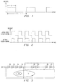
- pulse width, P, period, T, and frequency of a clock signal should remain the same from cycle to cycle. Due to noise generated in and in close proximity to the PLL circuit, however, the period can vary around a mean value. Fluctuation of the period of a clock signal relative to an ideal base is known as jitter. Since noise is the cause of this fluctuation, one may assume that jitter is a random statistical phenomena, Gaussian in nature.
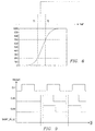
- Figure 2 illustrates a jittery clock compared with an ideal jitter-free clock.
- measured periods can be represented by [T 1 , T 2 , ... T n ].
- the mean period of the clock (T) is given by the equation:
- RMS jitter The standard deviation of the period is known as root mear square (RMS) jitter RMS jitter is given by the equation:
- duty ratio of the clock signal is defined as the ratio of pulse width to the period: P T
- TJD time jitter digitizer
- TJD circuits are fairly accurate in the sub-nanosecond range, they are expensive. Hence, it is not feasible to implement these TJD circuits in low-cost production testers, such as Texas Instrument'sTM V-series low-cost production testers. Accordingly, the TJD circuit is not commonly found in low-cost production testers.
- BIST circuitry implements the functions of an ATE on-chip by applying the test signal to the circuit under test (CUT) and analyzing its response to verify if the circuit is functioning properly. Due to the advancements in the process technology, the cost of implementing more functions on an integrated circuit is decreasing. The use of BIST circuitry leverages off of this advantage by reducing the production test time and allowing the use of low-cost testers in production testing. Thereby, BIST circuitry reduces the production test cost of integrated circuits.
- Sunter et al. presents another BIST scheme for measuring PLL specifications in the publication entitled "BIST for Phase-Locked Loops in Digtal Applications,” International Test Conference, IEEE Computer Society Press, p. 532-540 (1999). They also incorporate the use of a low-jitter clock as a reference to measure PLL jitter.
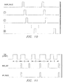
- the BIST scheme uses a string of inverters, 10-24, to delay the reference clock as shown in Figure 3. A portion of the delay chain is identified using digital logic such that the total delay of this portion is equal to peak-to-peak or the RMS jitter of the PLL.
- Two ring oscillators are then formed by connecting (1) all the inverters, 10-16, from the beginning of the delay chain to the beginning of the identified portion of the delay chain (T 1 ) or (2) all the inverters, 10-24, from the beginning of the delay chain to the end of the identified portion of the delay chain (T 2 ).
- This BIST scheme provides the measurement of the period of these ring oscillators where the peak-to-peak and RMS jitter is given by the difference between these periods.
- the delays of the inverters, however, during jitter measurement can be different from that when connected as ring oscillator due to interaction between the delay chain and the PLL. Thus, this arrangement has a tendency to lead to inaccurate jitter measurements.
- the BIST schemes described above assume the availability of a low-jitter reference clock. Yet, low-cost testers often do not include low-jitter clocks. Moreover, when low-jitter reference clocks are used, the clock signal must be routed carefully to the PLL since jitter can be injected into the clock signal in route to the PLL. Additionally, using on-chip oscillators for generating the clock signal is not recommended since its frequency and jitter can affect the BIST results. Furthermore, other proposed solutions are cost prohibitive and require significant vendor intrusion into one's design environment.
- the present invention teaches an integrated circuit chip having a built-in circuit for measuring error of a phase lock loop output clock signal.
- the circuit includes a short-pulse generator that generates a short-pulse signal having the same pulse width as the phase lock loop output clock signal.
- a delay chain including a plurality of delay elements, generates N delayed pulses from the short-pulse signal.
- a hit-pulse generator receives the N delayed pulses and compares each delayed pulse with the phase lock loop output clock signal 2 K times, such that the hit-pulse generator also generates a hit-pulse when both signals are high.
- a comparator compares a predetermined set of threshold values corresponding to the cumulative distribution of jitter for a PLL clock signal with the hit count.
- the storage unit stores the value of N.
- a processing unit calculates the error of the PLL clock signal using each stored value of N which directly relates to the cumulative distribution of jitter found in the PLL clock signal.
- Advantages of the present invention include but are not limited to an efficient, modular, testable BIST circuit which utilizes less time to test. Furthermore, since the BIST solution in accordance with the present invention is all-digital, it can be tested using standard digital test techniques. For a further savings, this BIST circuit is capable of running in tandem with other tests. Thus, a considerable amount of production test time can be saved for mixed-signal integrated circuits which use expensive mixed-signal ATEs.
- a BIST circuit in accordance with the present invention provides PLL testing in low-cost testers which aligns with the present and future technological needs of semiconductor testing. Particularly, since semiconductor manufacturers are advancing towards low cost testing and low cost testers where external reference clocks having low jitter may not be readily available.
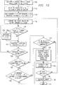
- FIG. 4 illustrates an embodiment of an all digital built-in self-test (BIST) circuit for phase locked loops (PLL) for measuring PLL jitter in sub-nano seconds constructed in accordance with the teachings fo the present invention.
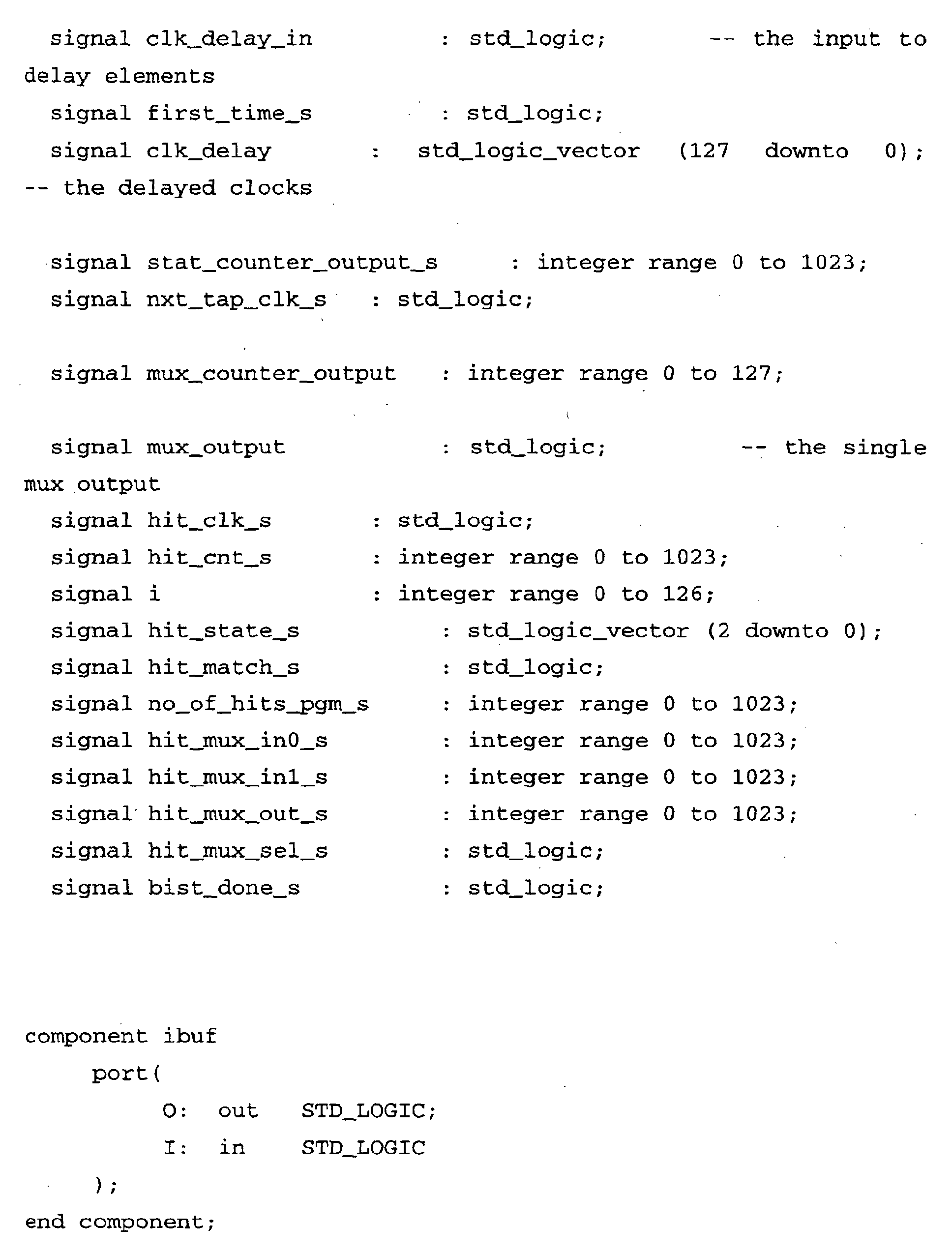
- Circuit 100 includes a short-pulse generator 104 which generates a short-pulse having the same frequency as the PLL clock which is fed into input 102.
- a delay chain 106 includes a plurality of delay elements for creating N delayed pulses from the short-pulse signal as shown.
- a multiplexer 108 receives the N delayed pulses into its inputs.
- a hit-pulse generator 114 receives the multiplexer 108 output signal and the phase lock loop output clock signal and generates a hit-pulse when both signals are high.
- a hit counter 116 counts the number of hit-pulses; thereby generating a hit-count.
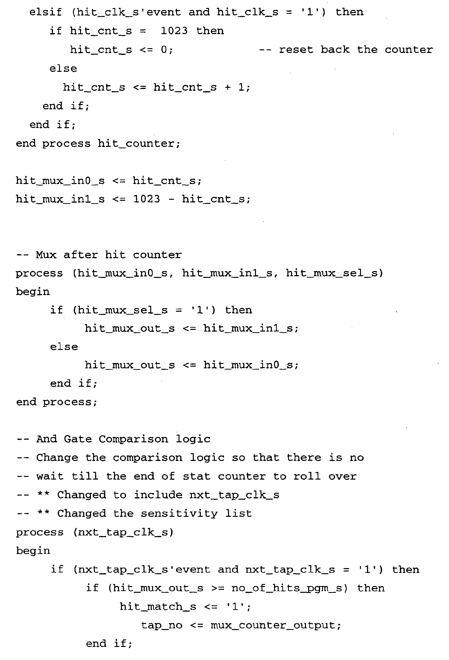
- a comparator 118 compares a pre-determined set of threshold values with the hit-count.
- the comparator 118 sends a signal to a storage unit 120 to store the value of the multiplexer counter 112.
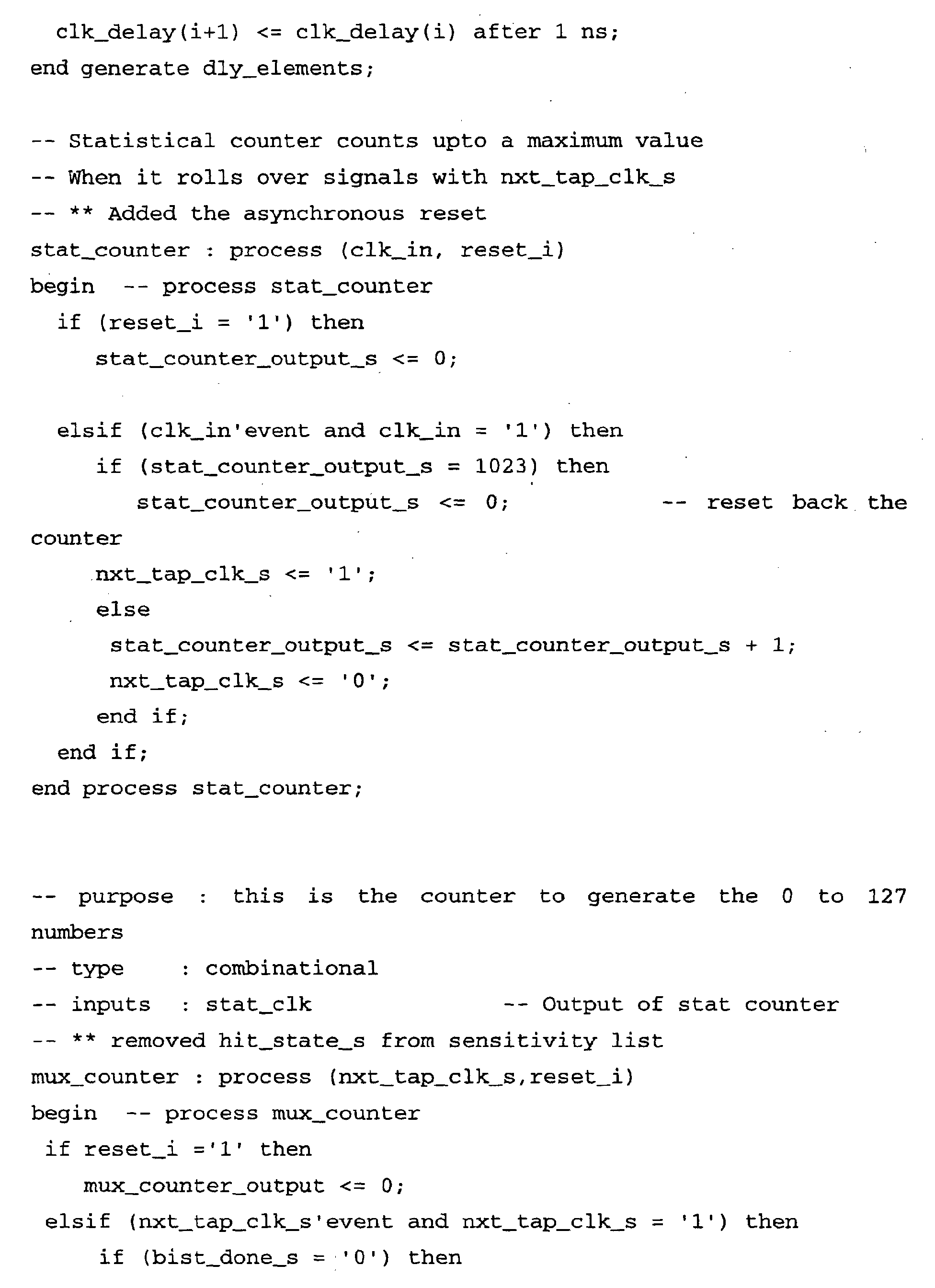
- a statistical counter 110 having a count from 1 to 2 k , couples to the multiplexer counter 112 and the hit-pulse generator 114 such that each of the N delayed pulses is compared with phase lock loop output clock signal 2 k times.
- a processing unit 122 couples to the storage unit 120 to calculate error of a phase lock loop output clock signal including the root means square of jitter for the phase lock loop output clock signal divided by the period, the peak-to-peak jitter for the phase lock loop output clock signal divided by the period and the duty ratio.
- circuit 100 uses the probability distribution of jitter and predetermined statistical values to make a determination of the error of the phase lock loop clock signal. Specifically, as shown in Figure 5, it it assumed that jitter follows a Gaussian distribution. Therefore, the rising edge of the clock signal can be anywhere between T1 and T2. The probability of the edge occurring at any time is given by the probability distribution of the jitter. If the jitter is gaussian, then the probability distribution is normal with mean T and the standard deviation is equal to the RMS jitter.
- Figure 6 illustrates that the number of times the clock is a "high” is proportional to the cumulative distribution function of the jitter probability distribution. Assuming the clock is observed for 1000 clock cycles, at time T1, the clock signal is "high” 200 times and the clock signal is “low” 800 times. At time T2, the clock signal is “high” 700 times and the clock signal is “low” 300 times. Thus, by use of the number of delays in the delay chain 106, the cumulative probability function of the jitter distribution can be derived.
- Figure 7 displays a plot of the number of times the clock is "high” at the end of each delay and against the number of delays up to that point.
- Use of the delay chain 106 with delays of equal amounts provides that the delay of a portion of the chain will be proportional to the number of delays in that portion.
- point n 1 represents the number of delays up to a point where the first "high” has occurred and point n 2 represents the number of delays up to a point where 500 "highs” have occurred.
- Point n 3 represents the number of delays up to a point where 841 "highs” have occurred and point n 4 represents the number of delays up to a point where 1000 "highs" have occurred.
- the ratio of the buffer delays can be controlled.
- the clock parameters are obtained as a ratio to the period. If it is necessary to convert the ratio to absolute time units, the mean PLL clock period can be measured using an ATE.
- n 1 n 6 are related to 2 k as displayed in the table below: Threshold Content of Mux Counter Comments 1 n 1 To measure peak-to-peak jitter 2 k X 0.5 n 2 To measure duty ratio and period 2 k X 0.84 n 3 To measure RMS jitter 2 k n 4 To measure peak-to-peak jitter 2 k X 0.5 n 5 To measure duty ratio 2 k X 0.5 n 6 To measure period When statistical counter 110 reaches its maximum value, a signal is issued that resets the hit counter 116 and increments multiplexer counter 112 to select the next delay buffer output.
- Advantages of the present invention include but are not limited to no requirement for a low-jitter reference clock nor ring oscillators. Since previous techniques measured edge jitter of the PLL, where edge jitter is defined as the jitter relative to a perfectly jitter free reference clock. Thus, the present invention provides more accurate measurement results than previous techniques.
- Figure 8 illustrates another embodiment of an all digital built-in self-test (BIST) circuit for phase locked loops (PLL) for measuring PLL jitter in sub-nano seconds constructed in accordance with the teachings of the present invention.
- Circuit 200 includes a short-pulse generator comprising delay block A 204 and delay block B 206 connected to an AND gate 208. It generates a short-pulse having the same frequency as the PLL clock which is fed into input 202.
- a delay chain 210 includes a plurality of delay elements 212-218 for creating N delayed pulses from the short-pulse signal as shown.
- a multiplexer 220 receives the N delayed pulses into its inputs.
- a multiplexer counter 222 having a count from 1 to N, controls the multiplexer 220 such that the multiplexer count detemines which of the N delayed pulses appears at the output of the multiplexer 220.
- AND gate 224 receives the multiplexer 108 output signal and the phase lock loop output clock signal and generates a hit-pulse when both signals are high.
- a hit counter 226 counts the number of hit-pulses; thereby generating a hit-count.
- An inverter 2228 receives the hit count. The inverted and non-inverted hit count are fed into a second multiplexer 230.
- the output of the multiplexer 230 couples into an AND gate 232 along with a predetermined set of threshold values such that when the hit count matches the predetermined threshold a control signal is sent to a storage unit 240 to store the multiplexer count 222.
- the control signal is also sent to a register 234 and compared with another register 236 having the value of the sample that will need to be inverted (in this case 5 or the binary number '101').
- AND gate 238 compares both values in registers 234 and 236. When the output of AND gate 238 is "high", the inverted hit count is passed through the multiplexer 230.
- Comparator 118 compares a pre-determined set of threshold values with the hit-count.
- a statistical counter 244 having a count from 1 to 2 k , couples to the multiplexer counter 222 and AND gate 224 such that each of the N delayed pulses is compared with phase lock loop output clock signal 2 k times.
- a processing unit 242 couples to the storage unit 240 to calculate error of a phase lock loop output clock signal including the root means square of jitter for the phase lock loop output clock signal divided by the period, the peak-to-peak jitter for the phase lock loop output clock signal divided by the period and the duty ratio.
- a short pulse is generated from the PLL output using delay block A 204 and delay block B 206 connected to an AND gate 208.
- the delay of each block, 204 and 206 is pre-determined during the design phase of the PLL and circuit 200.
- the delay of block B is ⁇ higher than the delay of block A.
- Delta ⁇ is typically required to be equal to the 1/100th of the period. Thus, for example, if the period of the PLL clock under test is 100ns, the delta will be 1ns.
- the delay of block A 204 may be 75ns and, hence, the delay of block B 206 will be 76ns (75ns + 1ns). As shown, these two delayed clocks are logically gated to generate the short-pulse signal.
- the short pulses are delayed by passing them through the delay chain 210 of non-inverting buffers.
- Delay chain 210 can also be realized using a transmission line structure in the IC.
- Figure 11 displays N delayed short-pulse signals.
- the individual output of each buffer can be selected using a multiplexer 220.
- appropriate output of the buffer is propagated to the output of the multiplexer 220.
- the output of the multiplexer 220 is compared against the PLL clock output using AND gate 224. If the PLL clock signal is high during the pulse, the hit-pulse signal is set high, which increments hit counter 226.
- a statistical counter 244 having a count from 1 to 2 k is implemented so that for each of the N delayed short-pulse signals sampling occurs 2 k times.
- the value for 2 k is set such that a large number of clock cycles is used to determine the characteristics of the jitter distribution. It is recommended that the statistical counter 244 be at least a 10-bit counter.
- STAT_MAX is issued which resets the hit counter 226 and increments the mux counter 222 to select the next delay buffer output.
- Figure 11 displays a timing diagram for the operation of this part of circuit 200.
- pulses generated from the rising edge of the jittery PLL clock CLK are delayed by a constant delay D using the delay chain 210.
- AND gate 224 generates a signal HIT_PULSE if CLK is high during the delayed pules.
- hit counter 226 will be incremented only 3 times during the 5 clock pulses. If this process is done until the statistical counter 244 saturates, the contents of the hit counter 226 will be proportional to the cumulative distribution function of the jitter.
- the contents of the hit counter 226 is compared with a pre-determined threshold T.
- This pre-determined threshold T is based on the theory explained above regarding Figure 7 and Table 1. If the value of the hit counter 226 is equal or greater than the pre-determined threshold T, then the value of the multiplexer counter 222 is stored in the storage unit 240.
- the hit counter 226 is sequentially compared with 6 different thresholds, as shown in Table 1.
- n 5 correlates to 2 k X 0.5 hits
- the content of the hit counter 226 is inverted before comparing it with the threshold T. Assuming that the statistical counter has k bits, these thresholds are given in Table 1.
- the recorded values of the multiplexer counter 222 can be scanned out to calculate the clock parameters using equations 5-7 listed above.
- Advantages of the present invention include but are not limited to an efficient, modular, testable BIST circuit which utilizes less time to test.
- the test time for measuring jitter in the range of 10s of pico seconds using TJD in Teradyne'sTM mixed-signal testers is estimated to be approximately 100ms.
- the test time for the BIST scheme according to the present invention is approximately 200X2000 clock cycles. Assuming 20MHZ clock, this translates to 20ms.
- a BIST circuit in accordance with the present invention provides PLL testing in low-cost testers which aligns with the present and future technological needs of semiconductor testing. Particularly, since semiconductor manufacturers are advancing towards low cost testing and low cost testers where external reference clocks having low jitter are not be readily available.
- a common concern about any BIST scheme is how to test the BIST circuit. Since the BIST solution in accordance with the present invention is all-digital, it can be tested using standard digital test techniques. If there is a parametric failure such as a lumped delay in the delay chain 210, path delay testing which can verify delays in 100s of pico seconds may be implemented to detect this failure.
- this BIST circuit is capable of running in tandem with other tests.
- a considerable amount of production test time can be saved for mixed-signal integrated circuits which use expensive mixed-signal ATEs.
- a BIST circuit in accordance with the present invention facilitates PLL testing on low-cost testers.
- Many ICs in ASIC are currently tested using V-series or VLCLT testers. These testers cannot measure PLL parameters like jitter and duty ratio. They just measure the PLL frequency during production testing. As the frequency of the PLL clock signals required for ICs increase, PLL specifications like jitter and duty ratio will become critical to the performance of these ICs.
- BIST circuits according to the present invention will help them to test their PLLs for jitter and duty ratio using low-cost testers.
- the ratio of delays in the delay chain 210 can be controlled tightly. Assuming that the ratio can be controlled up to 6-bits accurately, jitter will be equal to 10 buffer delays and the clock period will be equal to 200 buffer delays. Thereby, the error in jitter measurement will only be 3.17% compared to other approaches that estimate an error jitter measurement of ⁇ 50% in the pico-second range.
- Figure 12 illustrates a method for measuring jitter of phase locked loop (PLL) clocks in sub-nano seconds in accordance with the teachings of the present invention.
- step 100 a periodic train of short pulses from the PLL output is generated.
- step 112 dictates that series of N delayed signals should be generated from the short pulse signal of step 100.
- step 114 variables are set for the multiplexer counter, the hit counter, the statistical counter and state as shown.
- step 116 the original clock signal is compared with one of the N delayed signals. If, as indicated by step 118, both the clock signal and the delayed pulse are high, a hit signal is generated and, as is shown in step 120, the hit counter is incremented.
- step 122 the statistical counter is incremented.
- Step 124 determines whether the maximum number of the statistical count has been reached. If not, steps 118-124, repeat. If so, step 126 will determine if the state correspondes to the falling edge of the cummulative distribution of jitter in the clock signal. In the present embodiment, this state corresponds with the fifth sample point, n 5 (see Figure 7). If so, the hit count must be inverted prior to comparison with a predetermined threshold as indicated in step 130. Otherwise, the hit count is compared with the predetermined threshold as indicated in step 128. If the predetermined threshold has not been reached the multiplexer count and the state is incremented as shown in step 134.
- step 132 dictates that the state is incremented, the multiplexer count is stored in a storage unit and the threshold is changed to the next predetermined value. Afterwards, in step 134, the multiplexer count and the state are incremented as well.
- step 136 the state variable is compared to the maximum value of states for measuring jitter. In the present embodiment, this maximum value is seven, corresponding to point n 7 (see Figure 7). If the maximum value is reached, the error is calculated in step 138 and the subroutine ends in step 140; otherwise, steps 116 -136 are repeated.
- Step 112 indicates that N delayed signals are generated from the short pulse signal using a multiplexer and a multiplexer counter. Each of the N delayed signals are compared with the PLL clock signal 2 k times, where 2 k is a predetermined number, in steps 116 - 136. When the clock signal and the delayed signal are both high, a hit count is generated by the hit counter. Specifically, during steps 126 - 132, it is determined where both the hit count and the predetermined threshold value are the same and, as a result, the multiplexer counter value is stored. Jitter parameters are calculated in step 138 using the stored multiplexer counter values.
Landscapes
- Physics & Mathematics (AREA)
- Engineering & Computer Science (AREA)
- General Engineering & Computer Science (AREA)
- General Physics & Mathematics (AREA)
- Nonlinear Science (AREA)
- Tests Of Electronic Circuits (AREA)
- Stabilization Of Oscillater, Synchronisation, Frequency Synthesizers (AREA)
- Semiconductor Integrated Circuits (AREA)
- Manipulation Of Pulses (AREA)
Abstract
Description


| Threshold | Content of Mux Counter | Comments |
| 1 | n1 | To measure peak-to-peak jitter |
| 2k X 0.5 | n2 | To measure duty ratio and period |
| 2k X 0.84 | n3 | To measure RMS jitter |
| 2k | n4 | To measure peak-to-peak jitter |
| 2k X 0.5 | n5 | To measure duty ratio |
| 2k X 0.5 | n6 | To measure period |
| CLKA | CLKB | SHORT_PULSE |
| 0 | 0 | 0 |
| 0 | 1 | 0 |
| 1 | 0 | 1 |
| 1 | 1 | 0 |





Claims (20)
- An integrated circuit having a built-in self test circuit for measuring error of a phase lock loop output clock signal, comprising:a short-pulse generator coupled to receive the phase lock loop output clock signal to generate a short-pulse signal having the same pulse width as the phase lock loop output clock signal;a delay chain coupled to receive the short-pulse signal, the delay chain comprising a plurality of delay elements to generate N delayed pulses from the short-pulse signal;a hit-pulse generator coupled to receive the N delayed pulses to compare each of the N delayed pulses with the phase lock loop output clock signal 2k times, where k is a predetermined number and to generate a hit-pulse when both signals are high and to generate a hit count wherein the hit count is the number of hit pulses;a first comparator coupled to receive the hit count and at least one predetermined threshold value to compare the hit count for each of the N delayed pulses with the at least one predetermined threshold value;a storage unit coupled to the first comparator and the hit-pulse generator, such that when the hit count and one of the pre-determined set of threshold values are equivalent, the storage unit stores the value of N; anda processing unit coupled to the storage unit to calculate error of the phase lock loop output clock signal using each stored value of N for each corresponding predetermined threshold value.
- The integrated circuit chip having a built-in circuit for measuring error of a phase lock loop output clock signal as recited in claim 1 wherein the hit-pulse generator comprises:a multiplexer having a plurality of inputs and an output, the plurality of inputs coupled to receive the N delayed pulses;a first counter having a count from 1 to N, the first counter coupled to generate multiplexer count wherein the multiplexer count determines which of the N delayed pulses appears at the output of the multiplexer;a second comparator coupled to receive the multiplexer output signal and the phase lock loop output clock signal to generate a hit-pulse when both signals are high; anda second counter coupled to the hit-pulse generator to generate a hit count.
- The integrated circuit chip having a built-in circuit for measuring error of a phase lock loop output clock signal as recited in claim 1 wherein the short-pulse generator comprises:a first delay device having an input and an output, the input coupled to receive the phase lock loop output clock signal;a second delay device having an input and an output, the input coupled to receive the phase lock loop output clock signal, wherein the delay of the second delay device is larger then the delay of the first delay device; andan AND gate having an output, an inverting and non-inverting input, the non-inverting input coupled to the output of the first delay, the inverting input coupled to the output of the second delay, the output of the AND gate to provide the short-pulse signal.
- The integrated circuit chip having a built-in circuit for measuring error of a phase lock loop output clock signal as recited in claim 2 wherein the second comparator comprises an AND gate having a first and a second input and an output, the first input coupled to the output of the multiplexer, the second input coupled to receive the phase lock loop output clock signal, the AND gate couples to generate the hit-pulse at the output.
- The integrated circuit chip having a built-in circuit for measuring error of a phase lock loop output clock signal as recited in claim 2 wherein the second comparator comprises:an inverter having an input and an output, the input coupled to the output of the hit counter;a second multiplexer having a control input, a first and a second input, and an output, the first input coupled to output of the inverter, the second input coupled to the output of the hit counter; andan AND gate having a first and second input and an output, the first input coupled to the output of the second multiplexer, the second input coupled to receive the predetermined threshold.
- The integrated circuit chip having a built-in circuit for measuring error of a phase lock loop output clock signal as recited in claim 1 wherein the error value is the root means square of jitter for the phase lock loop output clock signal divided by the period.
- The integrated circuit chip having a built-in circuit for measuring error of a phase lock loop output clock signal as recited in claim 1 wherein the error value is the peak-to-peak jitter for the phase lock loop output clock signal divided by the period.
- The integrated circuit chip having a built-in circuit for measuring error of a phase lock loop output clock signal as recited in claim 1 wherein the error value is the duty ratio.
- The integrated circuit chip having a built-in circuit for measuring error of a phase lock loop output clock signal as recited in claim 1 wherein N > 1000.
- The integrated circuit chip having a built-in circuit for measuring error of a phase lock loop output clock signal as recited in claim 1 wherein 2k > 1000.
- The integrated circuit chip having a built-in circuit for measuring error of a phase lock loop output clock signal as recited in claim 1 wherein the number of predetermined threshold values is six corresponding to six points, n1-n6, that map one and a half periods of the cumulative distribution of jitter for the phase lock loop output clock signal, whereinn1 represents the point where the value of threshold is 1 at the start of the rising edge of the first period of the cumulative distribution,n2 represents the point where the value of threshold is 2k X 0.5 on the rising edge of the first period of the cumulative distribution,n3 represents the point where the value of threshold is 2k X 0.84 on the rising edge of the first period of the cumulative distribution,n4 represents the point where the value of threshold is 2k on the rising edge of the first period of the cumulative distribution,n5 represents the point where the value of threshold is 2k X 0.5 on the falling edge of the cumulative distribution, andn6 represents the point where the value of threshold is 2k X 0.5 on the rising edge of the second period of the cumulative distribution.
- The integrated circuit chip having a built-in circuit for measuring error of a phase lock loop output clock signal as recited in claim 11 wherein the error value is (n3-n2)/(n6-n2) where (n3-n2) represents the root means square of jitter of the phase lock loop output clock signal and (n6-n2) represents the period of the phase lock loop output clock signal.
- The integrated circuit chip having a built-in circuit for measuring error of a phase lock loop output clock signal as recited in claim 11 wherein the error value is (n4-n1)/(n6-n2) where (n4-n1) represents the peak-to-peak jitter of the phase lock loop output clock signal and (n6-n2) represents the period of the phase lock loop output clock signal.
- The integrated circuit chip having a built-in circuit for measuring error of a phase lock loop output clock signal as recited in claim 13 wherein each pulse of the plurality of N delayed pulses are less than one tenth of the peak-to-peak jitter of the phase lock loop output clock signal.
- The integrated circuit chip having a built-in circuit for measuring error of a phase lock loop output clock signal as recited in claim 11 wherein a duty ratio is (n5-n2) / (n6-n2) where (n5-n2) represents the average phase lock loop output pulse width of the phase lock loop output clock signal and (n6-n2) represents the period of the phase lock loop output clock signal.
- An integrated circuit chip having a built-in circuit for measuring error of a phase lock loop output clock signal, comprising:a first delay device having an input and an output coupled to receive the phase lock loop output clock signal;a second delay device having an input and an output coupled to receive the phase lock loop output clock signal, wherein the delay of the second delay device is larger then the delay of the first delay device;a first AND gate having an inverting and non-inverting input, the non-inverting input coupled to the output of the first delay, the inverting input coupled to the output of the second delay;a sorting circuit that includes a plurality of delay elements for creating N delayed pulses from the output of the first AND gate;a first multiplexer having a plurality of input signals and an output, the plurality of inputs coupled to receive the N delayed pulses;a first counter coupled to receive the phase lock loop output clock, wherein the first counter generates a statistical maximum count;a second counter having a control input and an output, the control input coupled to receive the statistical maximum count to generate a multiplexer count, the output of the second counter coupled to the first multiplexer;a second AND gate having a first and a second input and an output, the first input coupled to the output of the multiplexer, the second input coupled to receive the phase lock loop output clock signal;a third counter having a control input, an input and an output, the control input coupled to receive the statistical maximum count, the input of the third counter coupled to the output of the second AND gate;an inverter coupled to the output of the third counter;a second multiplexer having a control input, a first and a second input, and an output, the first input coupled to the inverter, the second input coupled to the output of the third counter;a third And gate having a first and second input and an output, the first input coupled to the output of the second multiplexer, the second input coupled to receive a predetermined threshold; anda storage unit coupled to the output of the third AND gate.
- A method for measuring jitter in a signal comprising the steps of:generating a short pulse signal from the signal;generating N delayed signals from the short pulse signal using a multiplexer and a multiplexer counter;comparing each of the N delayed signals with the signal 2k times, where 2k is a predetermined number;generating a hit count with a hit counter when both the clock signal and the delayed signal are high;comparing the hit count for each of the N delayed signals with a predetermined threshold value;storing the multiplexer counter value when both the hit count and the predetermined threshold value are equal; andcalculating error from the stored multiplexer counter values.
- The method of claim 17 wherein the error includes the root means square of jitter for the phase lock loop output clock signal divided by the period.
- The method of claim 17 wherein the error includes the peak-to-peak jitter for the phase lock loop output clock signal divided by the period.
- The method of claim 17 wherein the error includes the duty ratio.
Applications Claiming Priority (4)
| Application Number | Priority Date | Filing Date | Title |
|---|---|---|---|
| US19901800P | 2000-04-20 | 2000-04-20 | |
| US199018P | 2000-04-20 | ||
| US708994 | 2000-11-08 | ||
| US09/708,994 US6661266B1 (en) | 2000-11-08 | 2000-11-08 | All digital built-in self-test circuit for phase-locked loops |
Publications (3)
| Publication Number | Publication Date |
|---|---|
| EP1148340A2 true EP1148340A2 (en) | 2001-10-24 |
| EP1148340A3 EP1148340A3 (en) | 2004-01-07 |
| EP1148340B1 EP1148340B1 (en) | 2006-09-13 |
Family
ID=26894376
Family Applications (1)
| Application Number | Title | Priority Date | Filing Date |
|---|---|---|---|
| EP01201445A Expired - Lifetime EP1148340B1 (en) | 2000-04-20 | 2001-04-20 | All digital built-in self-test circuit for phase-locked loops |
Country Status (3)
| Country | Link |
|---|---|
| EP (1) | EP1148340B1 (en) |
| JP (1) | JP2002006003A (en) |
| DE (1) | DE60122960T2 (en) |
Cited By (6)
| Publication number | Priority date | Publication date | Assignee | Title |
|---|---|---|---|---|
| GB2387662A (en) * | 2002-03-02 | 2003-10-22 | Martin John Burbidge | Measurement of transfer function or step response for a phase locked loop |
| GB2393794A (en) * | 2002-10-01 | 2004-04-07 | Motorola Inc | Module, system and method for testing a phase locked loop |
| WO2006051438A1 (en) * | 2004-11-10 | 2006-05-18 | Koninklijke Philips Electronics N.V. | Testable integrated circuit |
| CN105527563A (en) * | 2014-09-30 | 2016-04-27 | 龙芯中科技术有限公司 | On-chip measuring circuit and measuring method |
| CN108572311A (en) * | 2017-03-14 | 2018-09-25 | 艾普凌科有限公司 | Semiconductor device |
| US11218153B1 (en) | 2020-10-29 | 2022-01-04 | Nxp B.V. | Configurable built-in self-test for an all digital phase locked loop |
Families Citing this family (6)
| Publication number | Priority date | Publication date | Assignee | Title |
|---|---|---|---|---|
| JP3887004B2 (en) * | 2003-05-30 | 2007-02-28 | 日本曹達株式会社 | Method for producing polymer |
| US20090219395A1 (en) * | 2005-08-29 | 2009-09-03 | Tektronix, Inc. | Measurement and Display for Video Peak Jitter with Expected Probability |
| US7495519B2 (en) * | 2007-04-30 | 2009-02-24 | International Business Machines Corporation | System and method for monitoring reliability of a digital system |
| DE102008059502A1 (en) * | 2008-11-28 | 2010-06-10 | Advanced Micro Devices, Inc., Sunnyvale | Compensation of the performance degradation of semiconductor devices by adjusting the duty cycle of the clock signal |
| US10514401B2 (en) * | 2017-08-02 | 2019-12-24 | Qualcomm Incorporated | On-chip frequency monitoring |
| KR102687631B1 (en) * | 2022-04-29 | 2024-07-23 | 주식회사 피델릭스 | Unit invertor propagatiom delay measuring circuit in semiconductor memory device |
Family Cites Families (4)
| Publication number | Priority date | Publication date | Assignee | Title |
|---|---|---|---|---|
| IT1210836B (en) * | 1987-06-26 | 1989-09-29 | Sip | INSTRUMENT FOR THE MEASUREMENT OF THE PHASE NOISE OF ANALOG SIGNALS |
| US5663991A (en) * | 1996-03-08 | 1997-09-02 | International Business Machines Corporation | Integrated circuit chip having built-in self measurement for PLL jitter and phase error |
| JPH10336024A (en) * | 1997-05-30 | 1998-12-18 | Nec Ic Microcomput Syst Ltd | Phase difference detecting device and semiconductor device having the same |
| US5889435A (en) * | 1997-06-30 | 1999-03-30 | Sun Microsystems, Inc. | On-chip PLL phase and jitter self-test circuit |
-
2001
- 2001-04-20 JP JP2001123055A patent/JP2002006003A/en not_active Abandoned
- 2001-04-20 EP EP01201445A patent/EP1148340B1/en not_active Expired - Lifetime
- 2001-04-20 DE DE60122960T patent/DE60122960T2/en not_active Expired - Lifetime
Cited By (10)
| Publication number | Priority date | Publication date | Assignee | Title |
|---|---|---|---|---|
| GB2387662A (en) * | 2002-03-02 | 2003-10-22 | Martin John Burbidge | Measurement of transfer function or step response for a phase locked loop |
| GB2393794A (en) * | 2002-10-01 | 2004-04-07 | Motorola Inc | Module, system and method for testing a phase locked loop |
| GB2393794B (en) * | 2002-10-01 | 2004-11-24 | Motorola Inc | Module, system and method for testing a phase locked loop |
| US7023195B2 (en) | 2002-10-01 | 2006-04-04 | Freescale Semiconductor, Inc. | Module, system and method for testing a phase locked loop |
| WO2006051438A1 (en) * | 2004-11-10 | 2006-05-18 | Koninklijke Philips Electronics N.V. | Testable integrated circuit |
| CN101052887B (en) * | 2004-11-10 | 2010-05-12 | Nxp股份有限公司 | testable integrated circuit |
| CN105527563A (en) * | 2014-09-30 | 2016-04-27 | 龙芯中科技术有限公司 | On-chip measuring circuit and measuring method |
| CN105527563B (en) * | 2014-09-30 | 2018-09-14 | 龙芯中科技术有限公司 | On piece measuring circuit and measurement method |
| CN108572311A (en) * | 2017-03-14 | 2018-09-25 | 艾普凌科有限公司 | Semiconductor device |
| US11218153B1 (en) | 2020-10-29 | 2022-01-04 | Nxp B.V. | Configurable built-in self-test for an all digital phase locked loop |
Also Published As
| Publication number | Publication date |
|---|---|
| EP1148340B1 (en) | 2006-09-13 |
| EP1148340A3 (en) | 2004-01-07 |
| DE60122960D1 (en) | 2006-10-26 |
| JP2002006003A (en) | 2002-01-09 |
| DE60122960T2 (en) | 2007-03-29 |
Similar Documents
| Publication | Publication Date | Title |
|---|---|---|
| US6661266B1 (en) | All digital built-in self-test circuit for phase-locked loops | |
| US7627790B2 (en) | Apparatus for jitter testing an IC | |
| US6807243B2 (en) | Delay clock generating apparatus and delay time measuring apparatus | |
| Sunter et al. | On-chip digital jitter measurement, from megahertz to gigahertz | |
| US6668346B1 (en) | Digital process monitor | |
| US20130305111A1 (en) | Circuit And Method For Simultaneously Measuring Multiple Changes In Delay | |
| CN101273559B (en) | Strobe technique for time stamping a digital signal | |
| US6670800B2 (en) | Timing variation measurements | |
| JP3625400B2 (en) | Test circuit for variable delay element | |
| US6185510B1 (en) | PLL jitter measuring method and integrated circuit therewith | |
| EP1148340B1 (en) | All digital built-in self-test circuit for phase-locked loops | |
| EP0909957A2 (en) | Measuring signals in a tester system | |
| US7408371B2 (en) | Apparatus for measuring on-chip characteristics in semiconductor circuits and related methods | |
| US7945404B2 (en) | Clock jitter measurement circuit and integrated circuit having the same | |
| US7856578B2 (en) | Strobe technique for test of digital signal timing | |
| US20060268970A1 (en) | Apparatus for measuring jitter and method of measuring jitter | |
| US7143323B2 (en) | High speed capture and averaging of serial data by asynchronous periodic sampling | |
| Tabatabaei et al. | An embedded core for sub-picosecond timing measurements | |
| JP2003179142A (en) | Semiconductor device equipped with jitter inspection circuit and jitter inspection method thereof | |
| US6470483B1 (en) | Method and apparatus for measuring internal clock skew | |
| US20090167317A1 (en) | Apparatus And Method For Test, Characterization, And Calibration Of Microprocessor-Based And Digital Signal Processor-Based Integrated Circuit Digital Delay Lines | |
| EP1927204A2 (en) | Strobe technique for time stamping a digital signal | |
| US20050022080A1 (en) | Systems and methods associated with test equipment | |
| US7254505B2 (en) | Method and apparatus for calibrating delay lines | |
| CN101359014B (en) | Built-in jitter measuring circuit |
Legal Events
| Date | Code | Title | Description |
|---|---|---|---|
| PUAI | Public reference made under article 153(3) epc to a published international application that has entered the european phase |
Free format text: ORIGINAL CODE: 0009012 |
|
| AK | Designated contracting states |
Kind code of ref document: A2 Designated state(s): AT BE CH CY DE DK ES FI FR GB GR IE IT LI LU MC NL PT SE TR |
|
| AX | Request for extension of the european patent |
Free format text: AL;LT;LV;MK;RO;SI |
|
| PUAL | Search report despatched |
Free format text: ORIGINAL CODE: 0009013 |
|
| AK | Designated contracting states |
Kind code of ref document: A3 Designated state(s): AT BE CH CY DE DK ES FI FR GB GR IE IT LI LU MC NL PT SE TR |
|
| AX | Request for extension of the european patent |
Extension state: AL LT LV MK RO SI |
|
| RIC1 | Information provided on ipc code assigned before grant |
Ipc: 7G 01R 31/3187 A |
|
| 17P | Request for examination filed |
Effective date: 20040707 |
|
| 17Q | First examination report despatched |
Effective date: 20040812 |
|
| AKX | Designation fees paid |
Designated state(s): DE FR GB |
|
| GRAP | Despatch of communication of intention to grant a patent |
Free format text: ORIGINAL CODE: EPIDOSNIGR1 |
|
| GRAS | Grant fee paid |
Free format text: ORIGINAL CODE: EPIDOSNIGR3 |
|
| GRAA | (expected) grant |
Free format text: ORIGINAL CODE: 0009210 |
|
| AK | Designated contracting states |
Kind code of ref document: B1 Designated state(s): DE FR GB |
|
| REG | Reference to a national code |
Ref country code: GB Ref legal event code: FG4D |
|
| REF | Corresponds to: |
Ref document number: 60122960 Country of ref document: DE Date of ref document: 20061026 Kind code of ref document: P |
|
| ET | Fr: translation filed | ||
| PLBE | No opposition filed within time limit |
Free format text: ORIGINAL CODE: 0009261 |
|
| STAA | Information on the status of an ep patent application or granted ep patent |
Free format text: STATUS: NO OPPOSITION FILED WITHIN TIME LIMIT |
|
| 26N | No opposition filed |
Effective date: 20070614 |
|
| REG | Reference to a national code |
Ref country code: FR Ref legal event code: PLFP Year of fee payment: 16 |
|
| REG | Reference to a national code |
Ref country code: FR Ref legal event code: PLFP Year of fee payment: 17 |
|
| PGFP | Annual fee paid to national office [announced via postgrant information from national office to epo] |
Ref country code: FR Payment date: 20170322 Year of fee payment: 17 |
|
| PGFP | Annual fee paid to national office [announced via postgrant information from national office to epo] |
Ref country code: GB Payment date: 20170328 Year of fee payment: 17 |
|
| PGFP | Annual fee paid to national office [announced via postgrant information from national office to epo] |
Ref country code: DE Payment date: 20170428 Year of fee payment: 17 |
|
| REG | Reference to a national code |
Ref country code: DE Ref legal event code: R119 Ref document number: 60122960 Country of ref document: DE |
|
| GBPC | Gb: european patent ceased through non-payment of renewal fee |
Effective date: 20180420 |
|
| PG25 | Lapsed in a contracting state [announced via postgrant information from national office to epo] |
Ref country code: DE Free format text: LAPSE BECAUSE OF NON-PAYMENT OF DUE FEES Effective date: 20181101 |
|
| PG25 | Lapsed in a contracting state [announced via postgrant information from national office to epo] |
Ref country code: GB Free format text: LAPSE BECAUSE OF NON-PAYMENT OF DUE FEES Effective date: 20180420 |
|
| PG25 | Lapsed in a contracting state [announced via postgrant information from national office to epo] |
Ref country code: FR Free format text: LAPSE BECAUSE OF NON-PAYMENT OF DUE FEES Effective date: 20180430 |