EP1147522B1 - Curved optical device and method of fabrication - Google Patents
Curved optical device and method of fabrication Download PDFInfo
- Publication number
- EP1147522B1 EP1147522B1 EP00903323A EP00903323A EP1147522B1 EP 1147522 B1 EP1147522 B1 EP 1147522B1 EP 00903323 A EP00903323 A EP 00903323A EP 00903323 A EP00903323 A EP 00903323A EP 1147522 B1 EP1147522 B1 EP 1147522B1
- Authority
- EP
- European Patent Office
- Prior art keywords
- optical
- layer
- optical layer
- backing plate
- adhesive
- Prior art date
- Legal status (The legal status is an assumption and is not a legal conclusion. Google has not performed a legal analysis and makes no representation as to the accuracy of the status listed.)
- Expired - Lifetime
Links
Images



Classifications
-
- G—PHYSICS
- G21—NUCLEAR PHYSICS; NUCLEAR ENGINEERING
- G21K—HANDLING OF PARTICLES OR IONISING RADIATION NOT OTHERWISE PROVIDED FOR; IRRADIATION DEVICES; GAMMA RAY OR X-RAY MICROSCOPES
- G21K1/00—Arrangements for handling particles or ionising radiation, e.g. focusing or moderating
- G21K1/06—Arrangements for handling particles or ionising radiation, e.g. focusing or moderating using diffraction, refraction or reflection, e.g. monochromators
-
- G—PHYSICS
- G21—NUCLEAR PHYSICS; NUCLEAR ENGINEERING
- G21K—HANDLING OF PARTICLES OR IONISING RADIATION NOT OTHERWISE PROVIDED FOR; IRRADIATION DEVICES; GAMMA RAY OR X-RAY MICROSCOPES
- G21K2201/00—Arrangements for handling radiation or particles
- G21K2201/06—Arrangements for handling radiation or particles using diffractive, refractive or reflecting elements
- G21K2201/067—Construction details
Definitions
- the present invention relates to novel methods of producing curved optical elements, in particular elements of extremely high precision, for use with soft and hard x rays, ultraviolet, visible, and infrared radiation and the optical elements achieved by these methods.
- Curved surfaces are used in a number of applications including but not limited to doubly curved crystals for x-ray applications, mirrors for ring laser gyros, and substrates for single or multilayer thin films.
- Doubly curved crystals are known to be useful as a focusing device for monochromatic x-ray or a wavelength dispersive device in an x-ray spectrometer.
- a toroidal curved crystal can provide point-to-point focusing of monochromatic x-rays, and a crystal curved to an ellipsoid can be used as a broad energy x-ray detection device.
- the present invention is directed to providing inexpensive high quality optical surfaces, and to methods of fabrication thereof.
- the present invention comprises in one aspect an optically curved element according to claim 1.
- a method for fabricating an optically curved element using a mold having a curved surface according to claim 18 is provided.
- the device is fabricated by providing an optically smooth flexible layer, securing the flexible layer to a surface of a mold having a desired optical doubly curved shape, providing an adhesive (wherein the method of securing the optical surface of the flexible layer to the mold prevents adhesive from contacting the surface of the mold), providing a backing plate on the adhesive and applying pressure to at least one of the backing plate and the mold to squeeze the adhesive and permanently conform the surface of the flexible layer to the surface of the mold, and thereafter, removing the mold to thereby produce the device.
- a novel curved optical element, and method of fabrication that acquires its shape from a reusable mold.
- the optical surface of the flexible layer need not conform exactly to a supporting surface of a backing plate.
- the backing plate can be removable from the rest of the optical element.
- an inexpensive optically curved surface can be fabricated in accordance with the principles of the present invention, i.e., because a reusable mold is employed, and since the backing plate curvature and surface finish are not critical.
- the use of a relatively thick epoxy layer allows the flexible layer to conform to a curved surface of the mold.
- relatively thick means that the thickness of the adhesive layer is greater than the thickness of the flexible layer having the optical surface to be curved.
- the smooth optical surface can be curved to any preselected geometry to comprise one of a convex surface, a concave surface, a toroidal surface, a parabolic surface, a spherical surface or an ellipsoidal surface.
- the optical surface can be a singularly curved surface or a doubly curved surface.
- the diffracting planes can be either inclined or parallel to the optical surface of the flexible layer.
- a curved optical device as shown in Fig. 1 comprises a flexible layer 10, a thick epoxy layer 12 and a backing plate 14.
- the structure of the device is shown by the vertical cross-sectional view in Fig. 2.
- the epoxy layer 12 holds and constrains the flexible layer 10 to a selected geometry having a curvature.
- the thickness of the epoxy layer is greater than 20 ⁇ m and the thickness of the flexible layer is greater than 5 ⁇ m. Further, the thickness of the epoxy layer is typically thicker than the thickness of the flexible layer.
- the flexible layer can be one of a large variety of materials, including: mica, Si, Ge, quartz, plastic, glass etc.
- the epoxy layer 12 can be a paste type with viscosity in the order of 10 3 to 10 4 poise and 30 to 60 minutes pot life.
- the backing plate 14 can be a solid object that bonds well with the epoxy.
- the surface 18 of the backing plate can be flat (Fig. 2) or curved as shown in Fig. 3, and its exact shape and surface finish are not critical to the shape and surface finish of the flexible layer. This is contrasted with standard fabrication practices which require a backing plate with a surface that is exactly the desired shape of the device.
- Another drawback to the standard approach is that each device requires a specially prepared backing plate. In the invention disclosed here, a specially prepared backing plate is not required.
- the surrounding of the flexible layer may be a thin sheet of protection material 16, such as a thin plastic, that is used around the flexible layer edge (see Fig. 2).
- the protection material protects the mold so that the mold is reusable.
- the protection material would not be necessary for a mold that is the exact size or smaller than the flexible layer or for a sacrificial mold.
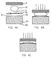
- the fabrication method of the curved optical device is schematically illustrated in Figs. 4a, 4b and 4c.
- the optically smooth flexible layer 10 is prepared and it may be a sheet with a smooth optical surface or a crystal sheet with diffracting planes parallel to the surface (see Fig. 5a) or with diffracting planes inclined to the surface (see Fig. 5b).
- thin sheet plastic protection material 16 such as tape
- the flexible layer with the thin plastic protection material 16 is positioned on a convex mold 20 which has an optically smooth surface 22 curved to a preselected geometry.
- the epoxy 12 is prepared and applied between the flexible layer and the backing plate.
- the thin plastic protection material 16 prevents the epoxy from contacting the mold surface 22 and bonding to the mold surface allowing the mold to be reused.
- a solid backing plate 14 is placed over the epoxy and a pressure is applied on the plate to squeeze the epoxy to conform the optically smooth surface of the flexible layer to the shape of surface 22.
- a preferred method is to gradually increase the pressure as the viscosity of the epoxy increases during the polymerization stage.
- the epoxy is at room temperature and pressure is applied mechanically in the span of about an hour. Curing time for the epoxy is approximately 24 hours, and the epoxy comprises a low shrinkage material, approximately 0.001"/inch.
- the thick epoxy layer undergoes high viscosity flow under pressure to conform the flexible layer on a convex mold curved to a pre-selected geometry.
- the epoxy layer is applied between the flexible layer and a backing plate.
- the pressure on the epoxy can be created by squeezing the epoxy using the backing plate.
- irregularities on the flexible layer can be eliminated and the shape of the flexible layer can be maintained when the epoxy is cured.
- the epoxy in a preferred embodiment has properties of low shrinkage, high viscosity, and high dimensional stability after setting. Alternatively, materials other than epoxies that meet these criteria can also be used for bonding and conforming the flexible layer.
- the mold of a preferred embodiment is made of glass or other light transparent materials so that the contact between the optically smooth surface of the flexible layer 24 and the convex surface 22 can be viewed from bottom surface 26.
- the unevenness of the optical surface of the flexible layer with respect to the convex surface 22 can be revealed by optical interference fringes under illumination of light through surface 26.
- the mold may be diamond turned to achieve a high quality mold surface.
- the shape of the flexible layer is determined by the shape of the mold surface.
- the flexible layer is permanently conformed to the curvature of the mold. The mold may be reused to make additional optically curved devices.
- the backing plate is carefully aligned to the mold during the fabrication process that allows for easy alignment of the optic.
- the edges of the backing plate or other registration points on the backing plate are used to find the center of the optic and/or the optic orientation for a curved optical element.
- Figs. 6a & 6b show the final configurations of devices corresponding to two types of the crystal slabs described in Figs. 5a & 5b, respectively.
- the crystal device has Johann geometry in the plane of Roland circle if the crystal slab used for fabrication is one of the types shown in Figs. 5a & 5b and the curvature of the mold in the corresponding plane is 2R, where R is the radius of the Roland circle.
- the diffracting planes of the crystal can be parallel (Fig. 6a) or inclined (Fig. 6b) to the surface of the crystal.
- a device having the diffraction plane inclined to the crystal surface has the property that the source and the image are asymmetrical in the Roland circle plane with respect to the crystal.
- the flexible layer's final curvature is determined by the curvature of the curved surface of the mold 22 and not directly by the shape of the backing plate. Therefore the curvature and the surface finish of the backing plate are not critical to the curvature and surface finish of the flexible layer.
- the curved surface of the mold 22 can be convex or concave and toroidal, spherical, ellipsoid, or other optical surfaces, and hence the flexible layer can be curved to any of these geometries.
- a crystal is used as the flexible layer is focusing a particular wavelength of x-rays from a small x-ray source.
- This type of device with point-to-point focusing property is illustrated in Fig. 7.
- the crystal in this device has a toroidal shape and the crystal satisfies Johann geometry in the plane of Rowland circle 28 and also has axial symmetry about the line joining source S and image I.
- An x-ray crystal device in accordance with the invention offers a highly uniform doubly bent crystal because of the elimination of the effects of irregularity occurring in a thin bonding layer in the prior art, and it gives better performance when used for x-ray optics applications.
Landscapes
- Physics & Mathematics (AREA)
- Spectroscopy & Molecular Physics (AREA)
- Engineering & Computer Science (AREA)
- General Engineering & Computer Science (AREA)
- High Energy & Nuclear Physics (AREA)
- Laminated Bodies (AREA)
- Heating, Cooling, Or Curing Plastics Or The Like In General (AREA)
- Casting Or Compression Moulding Of Plastics Or The Like (AREA)
- Diffracting Gratings Or Hologram Optical Elements (AREA)
- Optical Elements Other Than Lenses (AREA)
- Crystals, And After-Treatments Of Crystals (AREA)
- Analysing Materials By The Use Of Radiation (AREA)
- Surface Treatment Of Optical Elements (AREA)
Abstract
Description
- This application claims the benefit of U.S. Provisional Application No. 60/116,557 filed January 21, 1999. The provisional application is hereby incorporated by reference herein in its entirety.
- The present invention relates to novel methods of producing curved optical elements, in particular elements of extremely high precision, for use with soft and hard x rays, ultraviolet, visible, and infrared radiation and the optical elements achieved by these methods.
- Curved surfaces are used in a number of applications including but not limited to doubly curved crystals for x-ray applications, mirrors for ring laser gyros, and substrates for single or multilayer thin films.
- Doubly curved crystals are known to be useful as a focusing device for monochromatic x-ray or a wavelength dispersive device in an x-ray spectrometer. For example, a toroidal curved crystal can provide point-to-point focusing of monochromatic x-rays, and a crystal curved to an ellipsoid can be used as a broad energy x-ray detection device. Some of the prior art is described in EP-A-0200201 corresponding to U.S. 4,780,899 and EP.A. 0339713 corresponding to US.A. 4,949,367. These devices, having crystals bonded on a smooth concave substrate by a very thin layer of adhesive, have the drawback that the smoothness of the crystal planes is strongly affected by irregularities of the bonding layer. The irregularities can result from the lack of initial uniformity of the bonding layer on the substrate, or can occur during mounting of the crystal even if the initial adhesive layer is highly uniform. Another drawback is that a carefully prepared substrate is required for each curved surface.
- Thus, the present invention is directed to providing inexpensive high quality optical surfaces, and to methods of fabrication thereof.
- The present invention comprises in one aspect an optically curved element according to claim 1.
- In a further aspect, a method for fabricating an optically curved element using a mold having a curved surface according to
claim 18 is provided. - In a still further aspect, a method for fabricating an optically curved element is disclosed in claim 29.
- In one specific embodiment of the present invention, the device is fabricated by providing an optically smooth flexible layer, securing the flexible layer to a surface of a mold having a desired optical doubly curved shape, providing an adhesive (wherein the method of securing the optical surface of the flexible layer to the mold prevents adhesive from contacting the surface of the mold), providing a backing plate on the adhesive and applying pressure to at least one of the backing plate and the mold to squeeze the adhesive and permanently conform the surface of the flexible layer to the surface of the mold, and thereafter, removing the mold to thereby produce the device.
- To restate, provided herein is a novel curved optical element, and method of fabrication, that acquires its shape from a reusable mold. Advantageously, the optical surface of the flexible layer need not conform exactly to a supporting surface of a backing plate. Further, the backing plate can be removable from the rest of the optical element. Thus, an inexpensive optically curved surface can be fabricated in accordance with the principles of the present invention, i.e., because a reusable mold is employed, and since the backing plate curvature and surface finish are not critical. The use of a relatively thick epoxy layer allows the flexible layer to conform to a curved surface of the mold. As used herein, relatively thick means that the thickness of the adhesive layer is greater than the thickness of the flexible layer having the optical surface to be curved.
- In accordance with the present invention, the smooth optical surface can be curved to any preselected geometry to comprise one of a convex surface, a concave surface, a toroidal surface, a parabolic surface, a spherical surface or an ellipsoidal surface. The optical surface can be a singularly curved surface or a doubly curved surface. When the flexible layer comprises a crystal having diffracting planes, the diffracting planes can be either inclined or parallel to the optical surface of the flexible layer.
- The above-described objects, advantages and features of the present invention, as well as others, will be more readily understood from the following detailed description of certain preferred embodiments of the invention, when considered in conjunction with the accompanying drawings in which:
- Fig. 1 shows a simple form of the invention: a flexible layer comprising an optically smooth surface, a thick epoxy layer and a flat backing plate;
- Fig. 2 shows a vertical section view of Fig. 1;
- Fig. 3 shows a similar device with a flexible layer comprising an optically smooth surface, a thick epoxy layer and a concave backing plate;
- Fig. 4a shows a vertical cross-sectional view of an initial arrangement for fabrication of the device;
- Fig. 4b shows the configuration of a fabrication stage with the flexible layer being partially conformed;
- Fig. 4c shows the final stage of the fabrication with the optically smooth surface of the flexible layer conformed to the exact shape of the mold;
- Fig. 5a is a flat crystal sheet with flat diffracting atomic planes parallel to the crystal surface;
- Fig. 5b is a flat crystal sheet with flat diffracting planes inclined to the crystal surface;
- Fig. 6a is a vertical cross-section view of a crystal device using the type of crystal slab in Fig. 5a;
- Fig. 6b is a vertical cross-section view of a crystal device using the type of crystal slab in Fig. 5b; and
- Fig. 7 shows a toroidal crystal device with point-to-point focusing property.
- A curved optical device as shown in Fig. 1 comprises a
flexible layer 10, athick epoxy layer 12 and abacking plate 14. The structure of the device is shown by the vertical cross-sectional view in Fig. 2. In this device, theepoxy layer 12 holds and constrains theflexible layer 10 to a selected geometry having a curvature. Preferably, the thickness of the epoxy layer is greater than 20 µm and the thickness of the flexible layer is greater than 5 µm. Further, the thickness of the epoxy layer is typically thicker than the thickness of the flexible layer. The flexible layer can be one of a large variety of materials, including: mica, Si, Ge, quartz, plastic, glass etc. Theepoxy layer 12 can be a paste type with viscosity in the order of 103 to 104 poise and 30 to 60 minutes pot life. Thebacking plate 14 can be a solid object that bonds well with the epoxy. Thesurface 18 of the backing plate can be flat (Fig. 2) or curved as shown in Fig. 3, and its exact shape and surface finish are not critical to the shape and surface finish of the flexible layer. This is contrasted with standard fabrication practices which require a backing plate with a surface that is exactly the desired shape of the device. Another drawback to the standard approach is that each device requires a specially prepared backing plate. In the invention disclosed here, a specially prepared backing plate is not required. - The surrounding of the flexible layer may be a thin sheet of
protection material 16, such as a thin plastic, that is used around the flexible layer edge (see Fig. 2). The protection material protects the mold so that the mold is reusable. The protection material would not be necessary for a mold that is the exact size or smaller than the flexible layer or for a sacrificial mold. - The fabrication method of the curved optical device is schematically illustrated in Figs. 4a, 4b and 4c. In this method, the optically smooth
flexible layer 10 is prepared and it may be a sheet with a smooth optical surface or a crystal sheet with diffracting planes parallel to the surface (see Fig. 5a) or with diffracting planes inclined to the surface (see Fig. 5b). Then thin sheet plastic protection material 16 (such as tape) may be attached around the flexible layer edges as shown in Fig. 4a, then the flexible layer with the thinplastic protection material 16 is positioned on aconvex mold 20 which has an opticallysmooth surface 22 curved to a preselected geometry. The epoxy 12 is prepared and applied between the flexible layer and the backing plate. The thinplastic protection material 16 prevents the epoxy from contacting themold surface 22 and bonding to the mold surface allowing the mold to be reused. Asolid backing plate 14 is placed over the epoxy and a pressure is applied on the plate to squeeze the epoxy to conform the optically smooth surface of the flexible layer to the shape ofsurface 22. A preferred method is to gradually increase the pressure as the viscosity of the epoxy increases during the polymerization stage. During processing, the epoxy is at room temperature and pressure is applied mechanically in the span of about an hour. Curing time for the epoxy is approximately 24 hours, and the epoxy comprises a low shrinkage material, approximately 0.001"/inch. - The thick epoxy layer undergoes high viscosity flow under pressure to conform the flexible layer on a convex mold curved to a pre-selected geometry. The epoxy layer is applied between the flexible layer and a backing plate. The pressure on the epoxy can be created by squeezing the epoxy using the backing plate. As long as the flexible layer has good contact with the convex mold under pressure of the epoxy flow, irregularities on the flexible layer can be eliminated and the shape of the flexible layer can be maintained when the epoxy is cured. The epoxy in a preferred embodiment has properties of low shrinkage, high viscosity, and high dimensional stability after setting. Alternatively, materials other than epoxies that meet these criteria can also be used for bonding and conforming the flexible layer.
- The mold of a preferred embodiment is made of glass or other light transparent materials so that the contact between the optically smooth surface of the
flexible layer 24 and theconvex surface 22 can be viewed frombottom surface 26. The unevenness of the optical surface of the flexible layer with respect to theconvex surface 22 can be revealed by optical interference fringes under illumination of light throughsurface 26. When the epoxy is cured, the flexible layer with the epoxy and the backing plate are removed from the mold and the final device is made. The mold may be diamond turned to achieve a high quality mold surface. The shape of the flexible layer is determined by the shape of the mold surface. The flexible layer is permanently conformed to the curvature of the mold. The mold may be reused to make additional optically curved devices. - The backing plate is carefully aligned to the mold during the fabrication process that allows for easy alignment of the optic. The edges of the backing plate or other registration points on the backing plate are used to find the center of the optic and/or the optic orientation for a curved optical element.
- Figs. 6a & 6b show the final configurations of devices corresponding to two types of the crystal slabs described in Figs. 5a & 5b, respectively. The crystal device has Johann geometry in the plane of Roland circle if the crystal slab used for fabrication is one of the types shown in Figs. 5a & 5b and the curvature of the mold in the corresponding plane is 2R, where R is the radius of the Roland circle. The diffracting planes of the crystal can be parallel (Fig. 6a) or inclined (Fig. 6b) to the surface of the crystal. A device having the diffraction plane inclined to the crystal surface has the property that the source and the image are asymmetrical in the Roland circle plane with respect to the crystal.
- In this method, the flexible layer's final curvature is determined by the curvature of the curved surface of the
mold 22 and not directly by the shape of the backing plate. Therefore the curvature and the surface finish of the backing plate are not critical to the curvature and surface finish of the flexible layer. The curved surface of themold 22 can be convex or concave and toroidal, spherical, ellipsoid, or other optical surfaces, and hence the flexible layer can be curved to any of these geometries. - One significant application of this invention where a crystal is used as the flexible layer is focusing a particular wavelength of x-rays from a small x-ray source. This type of device with point-to-point focusing property is illustrated in Fig. 7. The crystal in this device has a toroidal shape and the crystal satisfies Johann geometry in the plane of
Rowland circle 28 and also has axial symmetry about the line joining source S and image I. - An x-ray crystal device in accordance with the invention offers a highly uniform doubly bent crystal because of the elimination of the effects of irregularity occurring in a thin bonding layer in the prior art, and it gives better performance when used for x-ray optics applications.
- While the invention has been described in detail herein in accordance with certain preferred embodiments thereof, many modifications and changes therein may be effected by those skilled in the art. Accordingly, it is intended by the appended claims to cover all such modifications and changes as fall within the scope of the invention.
Claims (30)
- An optically curved element comprising:a flexible optical layer (10) comprising an optical surface (24), the optical surface (24) of the optical layer (10) having a desired curvature, and the optical layer (10) having a thickness y; andan adhesive layer (12) disposed on a main surface of the optical layer (10) other than the optical surface (24) so as to conform the optical layer to a desired shape, the adhesive layer (12) having a minimum thickness x, wherein x > y.
- The optically curved element of claim 1, wherein the minimum thickness x of the adhesive layer (12) is greater than or equal to 20 µm. -
- The optically curved element of claim 1, wherein the thickness y of the optical layer (10) is greater than or equal to 5 µm.
- The optically curved element of claim 1, further comprising a backing plate (14) having a supporting surface (18), the adhesive layer (12) disposed above the supporting surface (18) of the backing plate (14).
- The optically curved element of claim 4, wherein the backing plate (14) comprises a cylindrical shape.
- The optically curved element of claim 4, wherein the supporting surface (18) of the backing plate (14) has a curvature, the curvature of the supporting surface (18) being different than the curvature of the optical surface (24) of the optical layer (10).
- The optically curved element of claim 4, wherein the optical surface (24) of the optical layer (10) is smoother than the supporting surface (18) of the backing plate (14).
- The optically curved element of claim 4, wherein the supporting surface (18) of the backing plate (14) comprises a planar surface.
- The optically curved element of claim 4, wherein the adhesive layer (12) comprises an epoxy material, and wherein the optically curved element further comprises a protective layer (16) surrounding an edge of the optical layer (10) such that the adhesive is disposed between the optical layer (10), with the protective layer (16) surrounding the edge thereof, and the supporting surface (18) of the backing plate (14).
- The optically curved element of claim 1, wherein the optical layer (10) having the optical surface (24) comprises one of a mica, silicon, germanium, quartz, glass, plastic or a crystalline material.
- The optically curved element of claim 1, wherein the optical surface (24) of the optical layer (10) comprises an optically smooth surface.
- The optically curved element of claim 1, wherein the optical surface (24) comprises at least one of a convex surface, concave surface, toroidal surface, parabolic surface, spherical surface or an ellipsoidal surface.
- The optically curved element of claim 1, wherein the optical surface (24) comprises one of a singularly curved surface or a doubly curved surface.
- The optically curved element of claim 1, wherein the optical layer (10) comprises a crystal having diffracting planes, the diffracting planes being either inclined or parallel to the optical surface (24) of the optical layer (10).
- The optically curved element of claim 1, wherein the optical surface (24) comprises an x-ray optical surface, and the optically curved element comprises a curved x-ray optical element.
- The optically curved element of claim 1, wherein the optical layer (10) has a uniform thickness, the uniform thickness comprising the thickness y.
- The optically curved element of claim 1, wherein the optical layer (10) comprises a crystal, the adhesive layer (12) is an epoxy, and wherein: 0.1 mm ≤ x ≤ 1 mm and 10 µm ≤ y ≤ 50 µm.
- A method for fabricating an optically curved element using a mold (20) having a curved surface (22), the method comprising:providing a flexible optical layer (10) having an optical surface (24);providing a backing plate (14) having a support surface (18) and disposing the flexible optical layer (10) between the supporting surface (18) of the backing plate (14) and the curved surface (22) of the mold (20);applying an adhesive between the flexible optical layer (10) and the supporting surface (18) of the backing plate (14); andapplying pressure to at least one of the backing plate (14) and the mold (20) to squeeze the adhesive and conform the flexible optical layer (10) to the curved surface (22) of the mold (20), thereby producing the optically curved element.
- The method of claim 18, wherein the optical surface (24) of the flexible optical layer (10) comprises one of a planar surface or curved surface prior to the applying of the pressure.
- The method of claim 18, wherein the adhesive comprises an epoxy, and wherein the method further comprises curing the epoxy while under pressure.
- The method of claim 20, further comprising increasing the pressure applied as viscosity of the epoxy increases during curing.
- The method of claim 18, wherein the mold (20) having the curved surface (22) is fabricated of a transparent material such that compression of the optical surface (24) of the flexible optical layer (10) is viewable through the mold (20).
- The method of claim 18, further comprising removing the mold (20) from contact with the optical surface (24) of the flexible optical layer (10) and subsequently reusing the mold (20) in a fabrication process for a separate optically curved element.
- The method of claim 18, further comprising providing the mold (20) with the curved surface (22), wherein the curved surface (22) is ground, diamond turned or polished to a precise, desired shape.
- The method of claim 18, wherein the flexible optical layer (10) has a surface area smaller than a surface area of the curved surface (22) of the mold (20), and wherein the method further comprises providing a protective material (16) adjacent at least one edge of the flexible optical layer (10) prior to disposing the adhesive between the flexible optical layer (10) and the supporting surface (18) of the backing plate (14), wherein the protective material (16) is sized and configured to prevent adhesive from contacting the curved surface (22) of the mold (20).
- The method of claim 25, wherein the protective material (16) comprises a flexible sheet material, the flexible sheet material comprising a tape.
- The method of claim 18, wherein the disposing of the adhesive comprises at least one of applying the adhesive to the flexible optical layer (10) or applying the adhesive to the supporting surface (18) of the backing plate (14).
- The method of claim 18, further comprising removing the mold (20) from contact with the optical surface (24) of the flexible optical layer (10), and after curving the adhesive, removing the backing plate (14) from contact with the adhesive, and subsequently reusing the backing plate (14) in a fabrication process for a separate optically curved element.
- A method for fabricating an optically curved element which can defract radiation of a desired wavelength, the method comprising:providing a backing plate (14) having a supporting surface (18);providing an adhesive layer (12) disposed above the supporting surface (18) of the backing plate (14), the adhesive layer (12) having a minimum thickness x; andproviding an flexible optical layer (10) disposed above the adhesive layer (12), the optical layer (10) comprising an optical surface (24), and conforming the optical surface (24) of the optical layer (10) to a desired curvature, the optical layer (10) having a thickness y, wherein x > y.
- The method of claim 29, further comprising removing the backing plate (14) from contact with the adhesive layer (12) after providing the optical layer (10) above the adhesive layer (12) conforming the optical surface (24) of the optical layer (10) to the desired curvature.
Applications Claiming Priority (5)
| Application Number | Priority Date | Filing Date | Title |
|---|---|---|---|
| US11655799P | 1999-01-21 | 1999-01-21 | |
| US116557P | 1999-01-21 | ||
| US09/342,606 US6285506B1 (en) | 1999-01-21 | 1999-06-29 | Curved optical device and method of fabrication |
| US342606 | 1999-06-29 | ||
| PCT/US2000/001139 WO2000044004A1 (en) | 1999-01-21 | 2000-01-18 | Curved optical device and method of fabrication |
Publications (2)
| Publication Number | Publication Date |
|---|---|
| EP1147522A1 EP1147522A1 (en) | 2001-10-24 |
| EP1147522B1 true EP1147522B1 (en) | 2006-03-29 |
Family
ID=26814365
Family Applications (1)
| Application Number | Title | Priority Date | Filing Date |
|---|---|---|---|
| EP00903323A Expired - Lifetime EP1147522B1 (en) | 1999-01-21 | 2000-01-18 | Curved optical device and method of fabrication |
Country Status (10)
| Country | Link |
|---|---|
| US (1) | US6285506B1 (en) |
| EP (1) | EP1147522B1 (en) |
| JP (2) | JP3955438B2 (en) |
| KR (1) | KR100466323B1 (en) |
| CN (1) | CN1151511C (en) |
| AT (1) | ATE322076T1 (en) |
| AU (1) | AU2508700A (en) |
| DE (1) | DE60026972T2 (en) |
| IL (2) | IL144440A0 (en) |
| WO (1) | WO2000044004A1 (en) |
Families Citing this family (31)
| Publication number | Priority date | Publication date | Assignee | Title |
|---|---|---|---|---|
| US6498830B2 (en) * | 1999-02-12 | 2002-12-24 | David B. Wittry | Method and apparatus for fabricating curved crystal x-ray optics |
| US6829327B1 (en) * | 2000-09-22 | 2004-12-07 | X-Ray Optical Systems, Inc. | Total-reflection x-ray fluorescence apparatus and method using a doubly-curved optic |
| EP1402541B1 (en) * | 2001-06-19 | 2006-08-16 | X-Ray Optical Systems, Inc. | Wavelength dispersive xrf system using focusing optic for excitation and a focusing monochromator for collection |
| US6781060B2 (en) | 2002-07-26 | 2004-08-24 | X-Ray Optical Systems Incorporated | Electrical connector, a cable sleeve, and a method for fabricating an electrical connection |
| ATE421152T1 (en) * | 2002-06-19 | 2009-01-15 | Xenocs | OPTICAL DEVICE FOR X-RAY APPLICATIONS |
| ATE488011T1 (en) * | 2002-08-02 | 2010-11-15 | X Ray Optical Sys Inc | OPTICAL DEVICE MADE OF A MULTIPLE CURVED OPTICAL CRYSTALS FOR FOCUSING X-RAYS |
| CN101520423B (en) * | 2003-03-27 | 2011-01-19 | 株式会社理学 | X-ray fluorescence analyzer |
| CN101356589B (en) * | 2005-08-01 | 2013-02-27 | 纽约州立大学研究基金会 | X-ray imaging systems employing point-focusing, curved monochromating optics |
| HU227011B1 (en) * | 2006-04-20 | 2010-04-28 | Mirrotron Kft | Method of manufacturing multi layers neutron guides |
| US7738629B2 (en) * | 2006-11-16 | 2010-06-15 | X-Ray Optical Systems, Inc. | X-ray focusing optic having multiple layers with respective crystal orientations |
| JP5344123B2 (en) * | 2008-07-18 | 2013-11-20 | 独立行政法人 宇宙航空研究開発機構 | X-ray reflector, X-ray reflector, and method for producing X-ray reflector |
| FR2935627B1 (en) * | 2008-09-10 | 2010-09-03 | Essilor Int | SURFACE TOOL WITH OPTICAL QUALITY |
| JP5125994B2 (en) * | 2008-11-04 | 2013-01-23 | 株式会社島津製作所 | Germanium curved spectroscopic element |
| US8130908B2 (en) * | 2009-02-23 | 2012-03-06 | X-Ray Optical Systems, Inc. | X-ray diffraction apparatus and technique for measuring grain orientation using x-ray focusing optic |
| CN102759765B (en) * | 2011-04-28 | 2014-11-05 | 北京兆阳光热技术有限公司 | Curved mirror reflector and production method thereof |
| US9057685B2 (en) | 2011-08-15 | 2015-06-16 | X-Ray Optical Systems, Inc. | Sample viscosity and flow control for heavy samples, and X-ray analysis applications thereof |
| CN103946693B (en) | 2011-10-06 | 2017-05-03 | X射线光学系统公司 | Mobile transport and shielding apparatus for removable x-ray analyzer |
| CN103765201B (en) | 2011-10-26 | 2017-11-07 | X射线光学系统公司 | Support structure for the X-ray analysis engine and analyzer and highly aligned monochromatic X-ray optics |
| EP2820666A4 (en) * | 2012-02-28 | 2016-02-17 | X Ray Optical Sys Inc | X-ray analyzer having multiple excitation energy bands produced using multi-material x-ray tube anodes and monochromating optics |
| WO2015027225A1 (en) | 2013-08-23 | 2015-02-26 | The Schepens Eye Research Institute, Inc. | Spatial modeling of visual fields |
| JP6069609B2 (en) * | 2015-03-26 | 2017-02-01 | 株式会社リガク | Double-curved X-ray condensing element and its constituent, double-curved X-ray spectroscopic element and method for producing the constituent |
| US10677744B1 (en) * | 2016-06-03 | 2020-06-09 | U.S. Department Of Energy | Multi-cone x-ray imaging Bragg crystal spectrometer |
| CN105914570A (en) * | 2016-06-16 | 2016-08-31 | 华中科技大学温州先进制造技术研究院 | Toric reflector non-stable waveguide hybrid laser resonant cavity |
| CN107415060B (en) * | 2017-09-26 | 2019-03-05 | 长沙理工大学 | Precision machining method for small-caliber rotation axis symmetrical optical curved surface element |
| JP7394464B2 (en) * | 2018-07-04 | 2023-12-08 | 株式会社リガク | Fluorescent X-ray analyzer |
| CN109163663B (en) * | 2018-09-11 | 2020-09-11 | 苏州如期光电科技有限公司 | Manufacturing method of long-focus large-off-axis-amount off-axis paraboloid |
| CN109702909B (en) * | 2019-01-17 | 2020-11-27 | 同济大学 | A clamping tool applied to the manufacture of spherical curved crystal and manufacturing method |
| US11972875B2 (en) | 2019-09-24 | 2024-04-30 | Convergent R.N.R. Ltd | X-ray optical arrangement |
| US20220201830A1 (en) | 2020-12-23 | 2022-06-23 | X-Ray Optical Systems, Inc. | X-ray source assembly with enhanced temperature control for output stability |
| CN113459314A (en) * | 2021-07-21 | 2021-10-01 | 钢研纳克检测技术股份有限公司 | Hyperboloid crystal forming device |
| US12247934B2 (en) | 2022-07-29 | 2025-03-11 | X-Ray Optical Systems, Inc. | Polarized, energy dispersive x-ray fluorescence system and method |
Family Cites Families (7)
| Publication number | Priority date | Publication date | Assignee | Title |
|---|---|---|---|---|
| US4599741A (en) | 1983-11-04 | 1986-07-08 | USC--Dept. of Materials Science | System for local X-ray excitation by monochromatic X-rays |
| US4679918A (en) * | 1984-10-23 | 1987-07-14 | Ace Ronald S | Ophthalmic glass/plastic laminated lens having photochromic characteristics and assembly thereof |
| NL8501181A (en) | 1985-04-24 | 1986-11-17 | Philips Nv | CRYSTAL FOR A ROENT GENAL ANALYSIS DEVICE. |
| NL8801019A (en) | 1988-04-20 | 1989-11-16 | Philips Nv | ROENTGEN SPECTROMETER WITH DOUBLE-CURVED CRYSTAL. |
| JPH02160517A (en) | 1988-12-14 | 1990-06-20 | Sumitomo Bakelite Co Ltd | Manufacture of grooved substrate for optical disk |
| US5646976A (en) | 1994-08-01 | 1997-07-08 | Osmic, Inc. | Optical element of multilayered thin film for X-rays and neutrons |
| US5843235A (en) | 1996-09-11 | 1998-12-01 | Honeywell Inc. | Apparatus for forming a deposited curver coating on a substrate and mirror |
-
1999
- 1999-06-29 US US09/342,606 patent/US6285506B1/en not_active Expired - Lifetime
-
2000
- 2000-01-18 JP JP2000595349A patent/JP3955438B2/en not_active Expired - Fee Related
- 2000-01-18 AU AU25087/00A patent/AU2508700A/en not_active Abandoned
- 2000-01-18 CN CNB00802927XA patent/CN1151511C/en not_active Expired - Fee Related
- 2000-01-18 EP EP00903323A patent/EP1147522B1/en not_active Expired - Lifetime
- 2000-01-18 IL IL14444000A patent/IL144440A0/en active IP Right Grant
- 2000-01-18 DE DE60026972T patent/DE60026972T2/en not_active Expired - Lifetime
- 2000-01-18 AT AT00903323T patent/ATE322076T1/en not_active IP Right Cessation
- 2000-01-18 WO PCT/US2000/001139 patent/WO2000044004A1/en not_active Ceased
- 2000-01-18 KR KR10-2001-7008164A patent/KR100466323B1/en not_active Expired - Fee Related
-
2001
- 2001-07-19 IL IL144440A patent/IL144440A/en not_active IP Right Cessation
-
2005
- 2005-10-31 JP JP2005316644A patent/JP2006139276A/en not_active Withdrawn
Also Published As
| Publication number | Publication date |
|---|---|
| IL144440A0 (en) | 2002-05-23 |
| ATE322076T1 (en) | 2006-04-15 |
| CN1337047A (en) | 2002-02-20 |
| IL144440A (en) | 2006-08-01 |
| JP3955438B2 (en) | 2007-08-08 |
| DE60026972D1 (en) | 2006-05-18 |
| EP1147522A1 (en) | 2001-10-24 |
| DE60026972T2 (en) | 2006-12-21 |
| JP2002535663A (en) | 2002-10-22 |
| KR100466323B1 (en) | 2005-01-15 |
| AU2508700A (en) | 2000-08-07 |
| CN1151511C (en) | 2004-05-26 |
| JP2006139276A (en) | 2006-06-01 |
| KR20010102966A (en) | 2001-11-17 |
| WO2000044004A1 (en) | 2000-07-27 |
| US6285506B1 (en) | 2001-09-04 |
Similar Documents
| Publication | Publication Date | Title |
|---|---|---|
| US6285506B1 (en) | Curved optical device and method of fabrication | |
| CN105074512B (en) | Curved diffraction gratings, its manufacture method and Optical devices | |
| TWI273968B (en) | A concave and convex component and a method of forming a die | |
| Said et al. | New developments in fabrication of high-energy-resolution analyzers for inelastic X-ray spectroscopy | |
| US3698795A (en) | Diffraction grating with two diffracting surfaces | |
| JPS60154014A (en) | Manufacture of optical element, executing device for said method and optical element manufactured through said method | |
| US4484798A (en) | Method of manufacturing a multiple mirror reflector for a land based telescope | |
| US6193898B1 (en) | Method and apparatus for fabricating reflector | |
| US6498830B2 (en) | Method and apparatus for fabricating curved crystal x-ray optics | |
| JP2628632B2 (en) | Crystal structure for X-ray spectroscopy and X-ray analyzer equipped with the crystal structure | |
| US6236710B1 (en) | Curved crystal x-ray optical device and method of fabrication | |
| JPS5932967Y2 (en) | lens support | |
| WO2016152940A1 (en) | Doubly curved x-ray condenser element, doubly curved x-ray spectroscopic element and apparatus equipped with same, and method for manufacturing said elements | |
| JP2002040628A (en) | Pellicle and method of bonding pellicle plate and pellicle frame | |
| JP4313675B2 (en) | Mirrors, optical imaging systems, and their use | |
| JPH07261010A (en) | Replica diffraction grating | |
| JP2002040629A (en) | Method of bonding pellicle plate and pellicle frame | |
| KR940004208B1 (en) | Method of manufacturing lens array optical system | |
| JP2001318300A (en) | Reflective optical system for optical antenna | |
| JPH04318501A (en) | Reflecting mirro device | |
| JP2006177994A (en) | Replica optical element | |
| US3466120A (en) | Method of making optical components | |
| JP4219609B2 (en) | Method for manufacturing polarization separating element | |
| KR100837027B1 (en) | Microlens array | |
| de Oliveira et al. | Composite material and optical fibres |
Legal Events
| Date | Code | Title | Description |
|---|---|---|---|
| PUAI | Public reference made under article 153(3) epc to a published international application that has entered the european phase |
Free format text: ORIGINAL CODE: 0009012 |
|
| 17P | Request for examination filed |
Effective date: 20010718 |
|
| AK | Designated contracting states |
Kind code of ref document: A1 Designated state(s): AT BE CH CY DE DK ES FI FR GB GR IE IT LI LU MC NL PT SE |
|
| AX | Request for extension of the european patent |
Free format text: AL;LT;LV;MK;RO;SI |
|
| RIN1 | Information on inventor provided before grant (corrected) |
Inventor name: CHEN, ZEWU |
|
| GRAP | Despatch of communication of intention to grant a patent |
Free format text: ORIGINAL CODE: EPIDOSNIGR1 |
|
| GRAS | Grant fee paid |
Free format text: ORIGINAL CODE: EPIDOSNIGR3 |
|
| RAP1 | Party data changed (applicant data changed or rights of an application transferred) |
Owner name: X-RAY OPTICAL SYSTEMS, INC. |
|
| GRAA | (expected) grant |
Free format text: ORIGINAL CODE: 0009210 |
|
| AK | Designated contracting states |
Kind code of ref document: B1 Designated state(s): AT BE CH CY DE DK ES FI FR GB GR IE IT LI LU MC NL PT SE |
|
| PG25 | Lapsed in a contracting state [announced via postgrant information from national office to epo] |
Ref country code: IT Free format text: LAPSE BECAUSE OF FAILURE TO SUBMIT A TRANSLATION OF THE DESCRIPTION OR TO PAY THE FEE WITHIN THE PRE;WARNING: LAPSES OF ITALIAN PATENTS WITH EFFECTIVE DATE BEFORE 2007 MAY HAVE OCCURRED AT ANY TIME BEFORE 2007. THE CORRECT EFFECTIVE DATE MAY BE DIFFERENT FROM THE ONE RECORDED.SCRIBED TIME-LIMIT Effective date: 20060329 Ref country code: BE Free format text: LAPSE BECAUSE OF FAILURE TO SUBMIT A TRANSLATION OF THE DESCRIPTION OR TO PAY THE FEE WITHIN THE PRESCRIBED TIME-LIMIT Effective date: 20060329 Ref country code: CH Free format text: LAPSE BECAUSE OF FAILURE TO SUBMIT A TRANSLATION OF THE DESCRIPTION OR TO PAY THE FEE WITHIN THE PRESCRIBED TIME-LIMIT Effective date: 20060329 Ref country code: AT Free format text: LAPSE BECAUSE OF FAILURE TO SUBMIT A TRANSLATION OF THE DESCRIPTION OR TO PAY THE FEE WITHIN THE PRESCRIBED TIME-LIMIT Effective date: 20060329 Ref country code: LI Free format text: LAPSE BECAUSE OF FAILURE TO SUBMIT A TRANSLATION OF THE DESCRIPTION OR TO PAY THE FEE WITHIN THE PRESCRIBED TIME-LIMIT Effective date: 20060329 |
|
| REG | Reference to a national code |
Ref country code: GB Ref legal event code: FG4D |
|
| REG | Reference to a national code |
Ref country code: CH Ref legal event code: EP |
|
| REG | Reference to a national code |
Ref country code: IE Ref legal event code: FG4D |
|
| REF | Corresponds to: |
Ref document number: 60026972 Country of ref document: DE Date of ref document: 20060518 Kind code of ref document: P |
|
| PG25 | Lapsed in a contracting state [announced via postgrant information from national office to epo] |
Ref country code: SE Free format text: LAPSE BECAUSE OF FAILURE TO SUBMIT A TRANSLATION OF THE DESCRIPTION OR TO PAY THE FEE WITHIN THE PRESCRIBED TIME-LIMIT Effective date: 20060629 Ref country code: DK Free format text: LAPSE BECAUSE OF FAILURE TO SUBMIT A TRANSLATION OF THE DESCRIPTION OR TO PAY THE FEE WITHIN THE PRESCRIBED TIME-LIMIT Effective date: 20060629 |
|
| PG25 | Lapsed in a contracting state [announced via postgrant information from national office to epo] |
Ref country code: ES Free format text: LAPSE BECAUSE OF FAILURE TO SUBMIT A TRANSLATION OF THE DESCRIPTION OR TO PAY THE FEE WITHIN THE PRESCRIBED TIME-LIMIT Effective date: 20060710 |
|
| PG25 | Lapsed in a contracting state [announced via postgrant information from national office to epo] |
Ref country code: PT Free format text: LAPSE BECAUSE OF FAILURE TO SUBMIT A TRANSLATION OF THE DESCRIPTION OR TO PAY THE FEE WITHIN THE PRESCRIBED TIME-LIMIT Effective date: 20060829 |
|
| REG | Reference to a national code |
Ref country code: CH Ref legal event code: PL |
|
| ET | Fr: translation filed | ||
| PG25 | Lapsed in a contracting state [announced via postgrant information from national office to epo] |
Ref country code: IE Free format text: LAPSE BECAUSE OF NON-PAYMENT OF DUE FEES Effective date: 20070118 |
|
| PG25 | Lapsed in a contracting state [announced via postgrant information from national office to epo] |
Ref country code: MC Free format text: LAPSE BECAUSE OF NON-PAYMENT OF DUE FEES Effective date: 20070131 |
|
| PLBE | No opposition filed within time limit |
Free format text: ORIGINAL CODE: 0009261 |
|
| STAA | Information on the status of an ep patent application or granted ep patent |
Free format text: STATUS: NO OPPOSITION FILED WITHIN TIME LIMIT |
|
| 26N | No opposition filed |
Effective date: 20070102 |
|
| PG25 | Lapsed in a contracting state [announced via postgrant information from national office to epo] |
Ref country code: GR Free format text: LAPSE BECAUSE OF FAILURE TO SUBMIT A TRANSLATION OF THE DESCRIPTION OR TO PAY THE FEE WITHIN THE PRESCRIBED TIME-LIMIT Effective date: 20060630 |
|
| PG25 | Lapsed in a contracting state [announced via postgrant information from national office to epo] |
Ref country code: LU Free format text: LAPSE BECAUSE OF NON-PAYMENT OF DUE FEES Effective date: 20070118 Ref country code: CY Free format text: LAPSE BECAUSE OF FAILURE TO SUBMIT A TRANSLATION OF THE DESCRIPTION OR TO PAY THE FEE WITHIN THE PRESCRIBED TIME-LIMIT Effective date: 20060329 |
|
| REG | Reference to a national code |
Ref country code: DE Ref legal event code: R082 Ref document number: 60026972 Country of ref document: DE Representative=s name: ANDRAE WESTENDORP PATENTANWAELTE PARTNERSCHAFT, DE Ref country code: DE Ref legal event code: R082 Ref document number: 60026972 Country of ref document: DE Representative=s name: FRIESE GOEDEN, DE Ref country code: DE Ref legal event code: R082 Ref document number: 60026972 Country of ref document: DE Representative=s name: FRIESE GOEDEN PATENTANWAELTE PARTGMBB, DE |
|
| REG | Reference to a national code |
Ref country code: FR Ref legal event code: PLFP Year of fee payment: 17 |
|
| REG | Reference to a national code |
Ref country code: DE Ref legal event code: R082 Ref document number: 60026972 Country of ref document: DE Representative=s name: FRIESE GOEDEN, DE Ref country code: DE Ref legal event code: R082 Ref document number: 60026972 Country of ref document: DE Representative=s name: FRIESE GOEDEN PATENTANWAELTE PARTGMBB, DE |
|
| REG | Reference to a national code |
Ref country code: FR Ref legal event code: PLFP Year of fee payment: 18 |
|
| PGFP | Annual fee paid to national office [announced via postgrant information from national office to epo] |
Ref country code: FI Payment date: 20170127 Year of fee payment: 18 |
|
| REG | Reference to a national code |
Ref country code: FR Ref legal event code: PLFP Year of fee payment: 19 |
|
| PGFP | Annual fee paid to national office [announced via postgrant information from national office to epo] |
Ref country code: NL Payment date: 20180126 Year of fee payment: 19 |
|
| PGFP | Annual fee paid to national office [announced via postgrant information from national office to epo] |
Ref country code: GB Payment date: 20180129 Year of fee payment: 19 |
|
| PGFP | Annual fee paid to national office [announced via postgrant information from national office to epo] |
Ref country code: FR Payment date: 20180125 Year of fee payment: 19 |
|
| PG25 | Lapsed in a contracting state [announced via postgrant information from national office to epo] |
Ref country code: FI Free format text: LAPSE BECAUSE OF NON-PAYMENT OF DUE FEES Effective date: 20180118 |
|
| PGFP | Annual fee paid to national office [announced via postgrant information from national office to epo] |
Ref country code: DE Payment date: 20190129 Year of fee payment: 20 |
|
| REG | Reference to a national code |
Ref country code: NL Ref legal event code: MM Effective date: 20190201 |
|
| GBPC | Gb: european patent ceased through non-payment of renewal fee |
Effective date: 20190118 |
|
| PG25 | Lapsed in a contracting state [announced via postgrant information from national office to epo] |
Ref country code: NL Free format text: LAPSE BECAUSE OF NON-PAYMENT OF DUE FEES Effective date: 20190201 Ref country code: FR Free format text: LAPSE BECAUSE OF NON-PAYMENT OF DUE FEES Effective date: 20190131 |
|
| PG25 | Lapsed in a contracting state [announced via postgrant information from national office to epo] |
Ref country code: GB Free format text: LAPSE BECAUSE OF NON-PAYMENT OF DUE FEES Effective date: 20190118 |
|
| REG | Reference to a national code |
Ref country code: DE Ref legal event code: R071 Ref document number: 60026972 Country of ref document: DE |